JP2004013633A - Non-contact ic card processor - Google Patents
Non-contact ic card processor Download PDFInfo
- Publication number
- JP2004013633A JP2004013633A JP2002167807A JP2002167807A JP2004013633A JP 2004013633 A JP2004013633 A JP 2004013633A JP 2002167807 A JP2002167807 A JP 2002167807A JP 2002167807 A JP2002167807 A JP 2002167807A JP 2004013633 A JP2004013633 A JP 2004013633A
- Authority
- JP
- Japan
- Prior art keywords
- contact
- processing unit
- card
- transport
- data processing
- Prior art date
- Legal status (The legal status is an assumption and is not a legal conclusion. Google has not performed a legal analysis and makes no representation as to the accuracy of the status listed.)
- Granted
Links
- 238000012545 processing Methods 0.000 claims abstract description 150
- 238000012546 transfer Methods 0.000 claims description 10
- 230000000007 visual effect Effects 0.000 claims description 4
- 238000004891 communication Methods 0.000 description 15
- 210000000078 claw Anatomy 0.000 description 7
- 238000003780 insertion Methods 0.000 description 7
- 230000037431 insertion Effects 0.000 description 7
- 238000012423 maintenance Methods 0.000 description 5
- 238000010586 diagram Methods 0.000 description 4
- 239000002184 metal Substances 0.000 description 4
- 238000009434 installation Methods 0.000 description 2
- 229920003002 synthetic resin Polymers 0.000 description 2
- 239000000057 synthetic resin Substances 0.000 description 2
- 229910000639 Spring steel Inorganic materials 0.000 description 1
- 239000003990 capacitor Substances 0.000 description 1
- 238000001816 cooling Methods 0.000 description 1
- 238000001514 detection method Methods 0.000 description 1
- 230000000694 effects Effects 0.000 description 1
- 238000000034 method Methods 0.000 description 1
Images




Landscapes
- Credit Cards Or The Like (AREA)
Abstract
Description
【0001】
【発明の属する技術分野】
本発明は、非接触ICカードを搬送しながらデータの読取り/書込み処理(以下、R/W処理とする)を行なう非接触ICカード処理装置に関し、特に、非接触ICカードの通信距離の長短に関係なくアンテナ部とデータ処理部を一体化してICデータ処理ユニットを配置できるようにした非接触ICカード処理装置に関する。
【0002】
【従来の技術】
近年、非接触ICカードは、パーキングカード、ポイントカード、定期券、入場券等、様々なカード類に適用されている。このようなカード類では、データのR/W処理と共に、その内容を目視できるよう表示することが必要な場合がある。この場合は、カード搬送路に沿ってR/W処理部と印字処理部を設け、R/W処理と目視データの印字処理を連続的に行なう構成の非接触ICカード処理装置が使用される。
【0003】
図7に、従来のこの種の非接触ICカード処理装置におけるR/W処理部の構成の概略を示す。
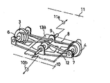
図7において、搬送方向に間隔を設けて配置された搬送ローラ1,2と非接触ICカード(図示せず)の搬送面Aを挟んで対向する押圧ローラ3,4が搬送面Aの上側に設けられる。各押圧ローラ3,4の向きが不揃いになることでカード搬送に支障が生じるのを防ぐために、図8に示ような梯子状の板バネ5で押圧ローラ3,4を連結すると共に、搬送ローラ1,2側に弾性付勢している。押圧ローラ3,4は、板バネ5に固定された支軸6,7に回転自由に設けられ、そのプーリ部にベルト8が巻回されている。板バネ5の中央部には支点軸9が固定されており、板金製の搬送路側壁10,11の貫通孔10a,11bに、前記支点軸9端部を貫通して板バネ5を搬送路側壁10,11に支持する。12は、支点軸9に回転自由に設けられたアイドラプーリで、板バネ5を避けてベルト8を張架するためのものである。押圧ローラ3,4の間の搬送路部分に配置されるICデータ処理ユニット13は、搬送路下方に配置されたデータ処理部13Aと、搬送面Aと板バネ5の間に配置されたアンテナ部13Bを備え、データ処理部13Aとアンテナ部13Bは配線14で電気的に接続されている。図1中、15a、15bは、搬送路に沿って適所に配置された位置検出用センサ(図中点線で示す)、15cはカードの向き及び表裏判定用センサ(図中点線で示す)、16は、搬送ローラ1を駆動するモータである。モータ16の動力は、ベルト17,18を介して搬送ローラ1に伝達され、搬送ローラ1に圧接する押圧ローラ3が回転し、ベルト8を介して押圧ローラ4が回転し、押圧ローラ4が圧接する搬送ローラ2が回転する。
【0004】
かかる構成の処理装置によるR/W処理動作を簡単に説明する。
挿入口19側から非接触ICカードが挿入され、センサ15aによりカードの挿入が検知されると、モータ16が駆動してカードがローラ2,4で挟持されて図1中左方向に搬送され、センサ15cでカード挿入方向及び表裏の検知が行なわれ、正しければ搬送動作を継続する。センサ15bでカードが検知されると、ICデータ処理ユニット13によりデータのR/W処理が実行される。R/W処理が終了すると、カードを図1中左方向に搬送して印字処理部による印字処理を実行する。両処理が終了すればカードを挿入口19側に返却する。
【0005】
【発明が解決しようとする課題】
ところで、非接触ICカードのICチップは多種多様で、通信距離の長いもの(通信距離25mm以上)もあれば短いもの(通信距離5〜10mm)もあり、この種の非接触ICカード処理装置は、様々な非接触ICカードに対応できるものが求められている。この場合、組立て作業性や組立て後のカード詰まり発生時の対応を考慮すれば、ICデータ処理ユニットとして、アンテナ部とデータ処理部を一体化して配置できることが望ましい。
【0006】
しかしながら、図7及び図8に示すような従来構造では、搬送面Aに近接してアンテナ部を配置する必要がある通信距離の短い非接触ICカードに対しては、センサ15c等があるために図7に示すように搬送面Aの上側で搬送面Aに近接してアンテナ部13Bを配置せざるを得ない。この場合、押圧ローラ3,4を連結する板バネ5が邪魔になりデータ処理部13Aの設置スペースがなく、ICでータ処理ユニット13をデータ処理部13Aとアンテナ部13Bに分離し、データ処理部13Aは図7に示すように搬送路下方に配置している。このため、アンテナ部13Bとデータ処理部13Aとの間に長い配線14が必要となり、組立てに手間がかかるという問題があった。また、組立て作業前にICデータ処理ユニット13のアンテナ部13Bとデータ処理部13Aを分離するため、両者の対応関係に食違いが生じないようにICデータ処理ユニットを管理する必要が生じる。
【0007】
更には、組立て後にカード詰まりが発生した場合、非接触ICカードを取り出すために板バネ5及びアンテナ部13Bを外して搬送路を開放するが、この場合に、アンテナ部13Bを取外す前に配線を外す必要があり、搬送路の開放に手間がかかる。
尚、アンテナ部を搬送面Aから離して配置できる通信距離の長い非接触ICカードに対しては、センサ15cより下方のスペースを利用して、アンテナ部とデータ処理部を一体化してICデータ処理ユニットを配置することが可能である。
【0008】
本発明は上記問題点に着目してなされたもので、非接触ICカードの通信距離の長短に関係なくアンテナ部とデータ処理部を一体化してICデータ処理ユニットの配置を可能とした非接触ICカード処理装置を提供することを目的とする。
【0009】
【課題を解決するための手段】
このため、請求項1の発明では、非接触ICカードの搬送路に沿って間隔を設けて配置される搬送ローラと搬送面を挟んで対向して搬送路上側に配置され、連結部材により互いに連結されて前記搬送ローラ側に弾性付勢される一対の押圧ローラを備え、該一対の押圧ローラ間の搬送路部分で、アンテナ部とデータ処理部を備えるICデータ処理ユニットにより前記非接触ICカードに対してデータの読取り/書込み処理を行なう非接触ICカード処理装置であって、前記連結部材を、両端部に前記押圧ローラを回転自由に設け中央部が搬送路から離れる方向に略コ字状に折曲された形状にすると共に、前記連結部材の上面側を介して押圧ローラを搬送ローラ側に弾性付勢する弾性部材を設ける構成とし、前記一対の押圧ローラ間の搬送路上方に、前記アンテナ部とデータ処理部を一体化した前記ICデータ処理ユニットを設置可能なスペースを形成したことを特徴とする。
【0010】
かかる構成では、一対の押圧ローラを連結する連結部材の中央部が搬送路から離れる方向に略コ字状に折曲されているので、一対の押圧ローラ間の搬送路部分の上方に従来より広いスペースが確保できる。このスペースに、アンテナ部とデータ処理部を一体化したICデータ処理ユニットを、アンテナ部を搬送面側に近接させるようにして配置できるようになる。
【0011】
請求項2の発明では、搬送路側壁の一方に着脱自由に係止する係止片を有し、搬送路側壁に係止した状態で下面が非接触ICカードの搬送をガイドするガイド部となるガイド部材を設け、該ガイド部材の搬送路側壁と反対側側面に突設したリテーナ部と前記連結部材の上面との間に、前記弾性部材を介在する構成とした。
【0012】
かかる構成では、ガイド部材の係止部を搬送路側壁から外すだけで、ガイド部材及び連結部材を取外すことができ、搬送路の開放が容易となる。
具体的には、請求項3のように、前記ガイド部材は、前記搬送面と略平行に伸びる前記連結部材の両端部上方にそれぞれ前記リテーナ部が突設され、前記連結部材の各端部上面と前記ガイド部材の各リテーナ部との間にそれぞれ前記弾性部材を介在する構成とするとよい。
【0013】
請求項4のように、アンテナ部とデータ処理部を一体化した前記ICデータ処理ユニットを、搬送路上方の前記スペースに前記アンテナ部を搬送面側に近接させて配置し、前記ガイド部材に固定する構成とすれば、通信距離の短い非接触ICカードに対してもデータのR/W処理が可能となる。また、ガイド部材を搬送路側壁から外せば、ICデータ処理ユニットも外れるので搬送路の開放がより一層容易になる。
【0014】
請求項5の発明では、前記ガイド部材は、その下面が前記搬送路の幅と略同等の幅を有し、該下面の搬送方向に沿った両端部を、非接触ICカードの搬送をガイドするガイド部とする構成である。
かかる構成では、ガイド部材を取付ければ、搬送路の両側に非接触ICカードの搬送をガイドするガイド部材の取付けができ、ガイド部材と反対側の搬送路側壁側に、ガイド部材とは別のガイド部材を取付ける必要がなくなり、組立て作業が容易となる。
【0015】
前記ガイド部材は、請求項6のように、前記ガイド部材は、搬送方向に沿って前記係止片を複数有する構成として、搬送路側壁から取外せるようにしてもよく、また、請求項7のように、搬送方向の一方の端部を、搬送面に対して上方向に回動可能なように前記搬送路側壁に軸支され、他方の端部に前記係止片を設ける構成として、搬送路の上方向に回動すれば搬送路が開放できるようにしてもよい。
【0016】
請求項2の構成において、請求項8のように、前記ICデータ処理ユニットでデータ処理された非接触ICカードに対して目視データを印字処理する印字処理部の搬送路の上側に、搬送面を挟んで搬送ローラと対向する押圧ローラを搬送ローラ側に押圧する加圧ユニットを設け、該加圧ユニットを取外すことで搬送路上側が開放される構成とするとよい。
【0017】
かかる構成では、R/W処理部の搬送路の開放が容易になるのに加えて印字処理部の搬送路の開放が容易となり、搬送路全体の開放が容易になり、カード詰まり発生時におけるカードの除去が極めて容易となる。
また、請求項9のように、前記一対の押圧ローラ間の搬送路下方に、前記アンテナ部とデータ処理部を一体化した前記ICデータ処理ユニットを設置可能なスペースを有する構成とすれば、ICデータ処理ユニットの設置場所を搬送路の上方にするか下方にするかを選択できるようになる。
【0018】
【発明の実施の形態】
以下、本発明の実施形態を図面に基づいて説明する。
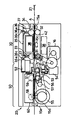
図1に、本発明に係る非接触ICカード処理装置の一実施形態の概略構成図を示す。尚、図7の従来例と同一部分には同一符号を付して説明を省略する。
図1において、本実施形態の非接触ICカード処理装置20は、挿入される非接触ICカード21に対してデータのR/W処理を行なうR/W処理部30と、R/W処理部30でデータ処理した非接触ICカード21の印刷領域に目視データの印字処理を行なう印字処理部50とを備える。
【0019】
R/W処理部30は、搬送路に沿って搬送面A下側に間隔を設けて配置された搬送ローラ31,32と、搬送面Aを挟んで搬送ローラ31,32と対向する押圧ローラ33,34と、押圧ローラ33,34を互いに連結し回転自由に支持する後述する合成樹脂製の連結部材35と、搬送路側壁の一方に着脱自由に係止して非接触ICカード21の搬送をガイドするための後述する合成樹脂製のガイド部材36と、ガイド部材36と連結部材35上面との間に介在して連結部材35を介して押圧ローラ33,34を搬送ローラ31,32側に押圧する弾性部材としてのコイルバネ37,37と、押圧ローラ33,34間の搬送路において非接触ICカード21に対してデータのR/W処理を行なうICデータ処理ユニット38と、従来と同様のセンサ15a〜15cと、モータ16とを備える。
【0020】
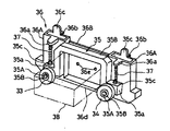
図2に、連結部材35及びガイド部材36の詳細を示す。
前記連結部材35は、各端部35a,35aが搬送面Aと略平行に伸び、中央部35bが搬送路から離れる方向に略コ字状に折曲された形状である。各端部35a,35aの側壁に、それぞれ支軸35A,35Aの一端が図3に示すように嵌合固定され、各支軸35A,35Aに軸受け35B,35Bを介して押圧ローラ33,34が回転自由に取付けられる。各端部35a,35aの上面には、コイルバネ37,37のリテーナ部35c,35cが突設されている。
【0021】
前記ガイド部材36は、両端部36A,36Aが上面開口の略箱状に形成され、中央部36Bが板状に形成されている。各端部36A,36Aには、一方の側壁上端部に図3に示すように下面に突設部を有しコイルバネ37,37の一端を保持するリテーナ部36a,36aが側方側に突設され、他方の側壁上端部に図3のように搬送路側壁39の通孔39aに着脱自由に係止する側方に突出した係止片36b,36bと、上方に突出した爪部36c,36cが形成されている。ガイド部材36の下面は、搬送路側壁39に係止した状態で非接触ICカード21の搬送をガイドするガイド部36dとなる。また、中央部36Bには、アンテナ部とデータ処理部を板金製のケースで一体に組付けて構成されるICデータ処理ユニット38(図2中、2点鎖線で示す)をネジ止めするための取付孔36e,36eが形成されている。また、図3に示すように、板金製の搬送路側壁39に対面する同じく板金製の他方の搬送路側壁39には、ガイド部材36と協働して非接触ICカード21の搬送をガイドするガイド部材40が固定されている。搬送路側壁39,39は、非接触ICカード21の搬送時における側面ガイドとなる。図3中の41は、処理装置20全体の制御を行なう制御ボードである。
【0022】
尚、搬送ローラ32は、図3に示すように、歯付きベルト42が巻き掛けられるローラ部と押圧ローラ34が圧接するローラ部が回転軸に固定されており、樹脂製の支持部に軸受けを介して回転軸が回転自由に軸支されている。搬送ローラ31は、モータ16側の駆動ベルト18を巻き掛けるプーリ部を備える以外は搬送ローラ32と同様の構成である。
【0023】
印字処理部50は、印字用サーマルヘッド51と、サーマルヘッド上方に配置される冷却ファン52と、サーマルヘッド51と搬送面Aを挟んで対向する印字用プラテンローラ53と、プラテンローラ53を駆動するソレノイド54と、搬送ローラ55,56と、アイドラプーリ57と、搬送面Aを挟んで搬送ローラ55,56と対向する押圧ローラ58,59を搬送ローラ側に押圧するため搬送路の上側に配置された加圧ユニット60と、図示しないカード発行部から供給される非接触ICカードを検出するためのセンサ15d,15e(図1中、破線で示す)を備える。
【0024】
前記加圧ユニット60は、本出願人により先に提案した例えば特願2001−298425号等に示された構成とするとよい。
即ち、押圧ローラ58,59をバネにより図1で下向きに常時弾性付勢された状態で軸支する加圧ユニット60に、2個の略U字状の弾性腕を互いに対向するように形成し、各弾性腕の先端部内側に突起を設ける。そして、各突起を例えば一方の搬送路側壁39(図1中で紙面背面側)に取付けた一対のブッシングの通孔にそれぞれ挿入することにより、加圧ユニット60が搬送路側壁39に対して図1中で紙面の背面側に回動自由に軸支されるようにする。また、加圧ユニット60の弾性腕側と反対側に2個の係止爪を設け、他方の搬送路側壁(図1中で紙面手前側)に取付けたバネ鋼からなるラッチの開口部に係止爪を係止することで加圧ユニット60を搬送路上方に閉じた状態で固定できるようになっている。従って、加圧ユニット60は、係止爪をラッチから外すだけで、搬送路側壁39に対して回動すれば搬送路上方を容易に開放できる構成である。
【0025】
かかる構成の非接触ICカード処理装置の動作について簡単に説明する。
モータ16の動力は、ベルト17,18を介して搬送ローラ31に伝達され、ベルト42を介して他方の搬送ローラ32に伝達され、コイルバネ37,37の弾性付勢力により搬送ローラ31,32に圧接する押圧ローラ33,34に伝達される。非接触ICカード21が挿入されセンサ15aによりカードの挿入が検知されると、モータ16が駆動して非接触ICカード21が装置内部に取込まれる。センサ15cでカード挿入方向及び表裏の検知が行なわれ、正しければ搬送動作を継続し、センサ15bでカードが検知されると、ICデータ処理ユニット38によりデータのR/W処理が実行され、R/W処理終了後、印字処理部50に搬送される。
【0026】
印字処理部50では、プラテンローラ53及び一方の搬送ローラ56を回転自由に軸支する支持部材61を、ソレノイド54により図1中上下方向に間欠的に駆動してプラテンローラ53を介して非接触ICカード21をサーマルヘッド51に圧接し印字を行なう。このソレノイド54の動作に同期させて、モータ16で駆動されるプラテンローラ53及び搬送ローラ55,56と加圧ユニット60の押圧ローラ58,59とにより非接触ICカード21の搬送動作を行い、非接触ICカード21の所定位置に印字を行なう。印字処理部50での印字処理終了後は、モータ16を逆転して非接触ICカード21を挿入口側に返却する。
【0027】
そして、本実施形態では、R/W処理部30において、搬送路上側に配置する押圧ローラ33,34の連結部材35を、その中央部35Bが搬送路から離れる方向に略コ字状に折曲する形状とすることで、搬送路上側に広い空間スペースを形成するようにした。これにより、アンテナ部を搬送路に近接させる必要がある通信距離の短い(通信距離5〜10mm)非接触ICカード対応の非接触ICカード処理装置の場合でも、アンテナ部上方にデータ処理部を板金製のケースで一体に組付けたICデータ処理ユニット38が図1に示すように実装可能である。
【0028】
このため、通信距離の長短に関係なく様々な非接触ICカードに対して、アンテナ部とデータ処理部を分離することなく、一体化したICデータ処理ユニット38を使用できる。従って、通信距離の短い非接触ICカード対応の処理装置とする場合に、アンテナ部とデータ処理部の対応関係を管理する必要がなくなる。また、アンテナ部とデータ処理部を個別に組付ける必要がなく、装置の組立て作業性が向上できる。
【0029】
また、ガイド部材36は、爪部36c,36cを図3中左方向に押して搬送路側壁39の通孔39aから係止片36b,36bを抜くだけで、搬送路側壁39から外せる。しかも、ICデータ処理ユニット38をガイド部材36の中央部36Bに取付ける構成であるので、ガイド部材36及び連結部材35の取外しと同時にIC処理ユニット38も取外せる。このため、カード詰まり発生時に搬送路上側を極めて簡単に開放でき、カード除去作業が容易となりメンテナンスが容易である。
【0030】
更に、本実施形態では、印字処理部50側も搬送路上側の加圧ユニット60の係止爪をラッチから外すだけで、搬送路上方を容易に開放できるので、R/W処理部30及び印字処理部50を含む非接触ICカード処理装置21の搬送路全体が容易に開放でき、カード詰まり発生時のカード除去等のメンテナンスが極めて容易である。
【0031】
ガイド部材の形状は図2のような形状に限るものでなく、図4〜図6にガイド部材のそれぞれ別の例を示す。
図4のガイド部材70は、図3において他方の搬送路側壁39側に取付けたガイド部材40を省略して、ガイド部材70の両側に非接触ICカードの搬送ガイド部71,71を形成するようにしたものである。その他の構成は、上述したガイド部材36と同様である。かかる構成のガイド部材70によれば、R/W処理部30における搬送路上側のガイド部材の取付け作業が、ガイド部材70を取付けるだけよく、非接触ICカード処理装置の組立て作業性が向上する。
【0032】
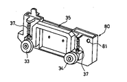
図5のガイド部材80は、ガイド部材80の一方の端部側に通孔81を設け、該通孔81に、搬送路側壁39に固定した回転軸(図示せず)を貫通させ、該回転軸回りに回動可能な構成である。その他の構成は、上述したガイド部材36と同様である。かかる構成のガイド部材80は、他方の係止片を搬送路側壁39から外し、回転軸回りにガイド部材80を回動すれば、搬送路上側を開放することができる。
【0033】
図6のガイド部材90は、その中央部90Aを、連結部材35の形状に合わせて略コ字状に折曲形成するようにしたものである。その他の構成は、上述したガイド部材36と同様である。かかる構成のガイド部材90の場合は、ICデータ処理ユニット38をガイド部材90ではなく搬送路側壁39側に取付ける。このため、搬送路上側を開放する場合に、ガイド部材90とIC処理ユニット38を別々に取外す必要があり、図2〜図5のガイド部材36,70,80に比べて搬送路上側の開放作業に手間がかかるが、IC処理ユニット38がアンテナ部とデータ処理部が一体化されているので、従来構造に比べれば、アンテナ部とデータ処理部間の配線取外し作業等がない分だけ搬送路上側の開放作業が容易となる。
【0034】
尚、本発明の非接触ICカード処理装置は、通信距離の長い(通信距離25mm以上)非接触ICカードに対応する場合も、R/W処理部30における押圧ローラ33,34間の搬送路上側のスペースにICデータ処理ユニット38を配置してもよいが、従来と同様に図1に2点鎖線で示すように、押圧ローラ33,34間の搬送路下方にも、アンテナ部とデータ処理部を一体化したICデータ処理ユニット38を配置可能なスペースを有するので、押圧ローラ33,34間の搬送路下方にICデータ処理ユニット38を配置することは可能である。
【0035】
【発明の効果】
以上説明したように本発明によれば、一対の押圧ローラの連結部材の形状を工夫することにより、搬送路上方にアンテナ部とデータ処理部を一体化したICデータ処理ユニットを配置できるようにしたので、アンテナ部を搬送面に近接する必要がある通信距離の短い非接触ICカードに対応する場合でもICデータ処理ユニットのアンテナ部とデータ処理部を一体化して組付けできる。従って、IC処理ユニットの組付け作業性を向上できるだけでなく、アンテナ部とデータ処理部の対応関係の管理が不要になる利点を有する。また、ICデータ処理ユニットを搬送路上側に配置した場合でも、ICデータ処理ユニットの取外しが容易で搬送路の開放が容易となり、カード詰まり発生時におけるカード除去等のメンテナンス作業が容易となる。
【0036】
また、搬送路側壁に着脱自由に係止させたガイド部材にICデータ処理ユニットを取付けることにより、ガイド部材と一体にICデータ処理ユニットの取外しができるので、より一層搬送路の開放作業が容易となりメンテナンス作業が容易となる。
更に、印字処理部の搬送路の上側に取外しが容易な加圧ユニットを設ける構成とすれば、非接触ICカード処理装置の搬送路全体を容易に開放でき、カード除去等のメンテナンス作業性がより一層向上する。
【図面の簡単な説明】
【図1】本発明に係る非接触ICカード処理装置の一実施形態の概略構成図
【図2】同上実施形態の連結部材及びガイド部材の説明図
【図3】ガイド部材の係止状態を示す断面図
【図4】ガイド部材の別の構成例を示す斜視図
【図5】ガイド部材の別の構成例を示す斜視図
【図6】ガイド部材の別の構成例を示す斜視図
【図7】従来装置のR/W処理部の概略構成図
【図8】従来の押圧ローラの連結構造の説明図
【符号の説明】
20 非接触ICカード処理装置
30 R/W処理部
31,32 搬送ローラ
33,34 押圧ローラ
35 連結部材
36,70,80,90 ガイド部材
36a リテーナ部
36b 係止片
36c 爪部
37 コイルバネ
38 ICデータ処理ユニット
39 搬送路側壁
50 印字処理部
60 加圧ユニット[0001]
TECHNICAL FIELD OF THE INVENTION
The present invention relates to a non-contact IC card processing device that performs data read / write processing (hereinafter, referred to as R / W processing) while transporting the non-contact IC card. The present invention relates to a non-contact IC card processing device in which an antenna unit and a data processing unit are integrated and an IC data processing unit can be arranged regardless of the configuration.
[0002]
[Prior art]
In recent years, non-contact IC cards have been applied to various cards such as parking cards, point cards, commuter passes, and admission tickets. In such cards, it is sometimes necessary to display the contents so that the contents can be viewed together with the R / W processing of the data. In this case, a non-contact IC card processing apparatus having a configuration in which an R / W processing section and a print processing section are provided along the card transport path and the R / W processing and the visual data printing processing are continuously performed is used.
[0003]
FIG. 7 schematically shows the configuration of an R / W processing unit in a conventional non-contact IC card processing apparatus of this type.
In FIG. 7, pressing
[0004]
An R / W processing operation by the processing device having such a configuration will be briefly described.
When the non-contact IC card is inserted from the
[0005]
[Problems to be solved by the invention]
By the way, the IC chips of the non-contact IC card are various, some of which have a long communication distance (communication distance of 25 mm or more) and some of which have a short communication distance (communication distance of 5 to 10 mm). There is a demand for a card that can handle various non-contact IC cards. In this case, it is desirable that the antenna unit and the data processing unit can be integrally disposed as an IC data processing unit in consideration of the workability of assembling and the measures to be taken when a card jam occurs after the assembling.
[0006]
However, in the conventional structure as shown in FIGS. 7 and 8, a non-contact IC card having a short communication distance, in which the antenna section needs to be arranged close to the transfer surface A, has the
[0007]
Further, when the card is clogged after assembling, the leaf spring 5 and the
For a non-contact IC card having a long communication distance in which the antenna unit can be arranged at a distance from the transfer surface A, the antenna unit and the data processing unit are integrated by using a space below the
[0008]
SUMMARY OF THE INVENTION The present invention has been made in view of the above-mentioned problems, and a non-contact IC in which an antenna unit and a data processing unit are integrated to enable an arrangement of an IC data processing unit regardless of a communication distance of the non-contact IC card. It is an object to provide a card processing device.
[0009]
[Means for Solving the Problems]
Therefore, according to the first aspect of the present invention, the non-contact IC cards are arranged on the upper side of the transport path opposite to the transport rollers arranged at intervals along the transport path of the non-contact IC card with the transport surface interposed therebetween, and are connected to each other by the connecting member. A pair of pressing rollers elastically urged toward the conveying roller side, and a non-contact IC card by an IC data processing unit including an antenna unit and a data processing unit in a conveying path portion between the pair of pressing rollers. A non-contact IC card processing device for performing data read / write processing on the other hand, wherein the connecting member is provided with the pressing rollers rotatably at both ends so as to have a substantially U-shape in a direction in which a central portion is away from the conveyance path. In addition to having a bent shape, an elastic member is provided to elastically urge the pressing roller toward the conveying roller through the upper surface of the connecting member, and the elastic member is provided above the conveying path between the pair of pressing rollers. , Characterized in that the IC data processing unit that integrates the antenna unit and a data processing unit to form a space capable of installation.
[0010]
In such a configuration, since the central portion of the connecting member that connects the pair of pressing rollers is bent in a substantially U-shape in a direction away from the conveying path, the central portion is wider than the conventional one above the conveying path portion between the pair of pressing rollers. Space can be secured. In this space, an IC data processing unit in which the antenna unit and the data processing unit are integrated can be arranged such that the antenna unit is close to the transport surface side.
[0011]
According to the second aspect of the present invention, one of the side walls of the transport path has a locking piece that is detachably engaged with the transport path side wall, and the lower surface of the locking section on the side wall of the transport path guides the transport of the non-contact IC card. A guide member is provided, and the elastic member is interposed between a retainer protruding from a side surface of the guide member opposite to a side wall of the conveyance path and an upper surface of the connecting member.
[0012]
In such a configuration, the guide member and the connecting member can be removed simply by removing the locking portion of the guide member from the side wall of the transport path, and the transport path can be easily opened.
Specifically, as in
[0013]
The IC data processing unit in which an antenna unit and a data processing unit are integrated as in claim 4, wherein the antenna unit is disposed in the space above a transport path, close to a transport surface side, and fixed to the guide member. With this configuration, data R / W processing can be performed even for a non-contact IC card having a short communication distance. Further, if the guide member is removed from the side wall of the transfer path, the IC data processing unit is also removed, so that the opening of the transfer path is further facilitated.
[0014]
In the invention according to claim 5, the lower surface of the guide member has a width substantially equal to the width of the transport path, and guides the non-contact IC card at both ends along the transport direction of the lower surface. The configuration is a guide portion.
In such a configuration, if a guide member is attached, a guide member for guiding the transport of the non-contact IC card can be attached to both sides of the transport path, and another side of the transport path side wall opposite to the guide member is provided with another guide member. There is no need to attach a guide member, and the assembling work is facilitated.
[0015]
The guide member may be configured such that the guide member has a plurality of the locking pieces along the transport direction so that the guide member can be detached from the side wall of the transport path. As described above, one end of the conveyance direction is supported by the side wall of the conveyance path so as to be rotatable upward with respect to the conveyance surface, and the locking piece is provided at the other end. The transport path may be opened by turning the path upward.
[0016]
In the configuration of claim 2, as in
[0017]
With this configuration, the transport path of the R / W processing unit can be easily opened, and in addition, the transport path of the print processing unit can be easily opened, and the entire transport path can be easily opened. Is extremely easy to remove.
According to a ninth aspect of the present invention, there is provided a configuration in which a space is provided below the conveyance path between the pair of pressing rollers so that the IC data processing unit in which the antenna unit and the data processing unit are integrated can be installed. It is possible to select whether the installation location of the data processing unit is above or below the transport path.
[0018]
BEST MODE FOR CARRYING OUT THE INVENTION
Hereinafter, embodiments of the present invention will be described with reference to the drawings.
FIG. 1 shows a schematic configuration diagram of one embodiment of a non-contact IC card processing device according to the present invention. The same parts as those in the conventional example of FIG.
In FIG. 1, a non-contact IC
[0019]
The R /
[0020]
FIG. 2 shows details of the connecting
The connecting
[0021]
The
[0022]
As shown in FIG. 3, the
[0023]
The
[0024]
The pressurizing
That is, two substantially U-shaped elastic arms are formed so as to face each other on a
[0025]
The operation of the non-contact IC card processing device having such a configuration will be briefly described.
The power of the
[0026]
In the
[0027]
In the present embodiment, in the R /
[0028]
Therefore, the integrated IC
[0029]
Further, the
[0030]
Further, in the present embodiment, the
[0031]
The shape of the guide member is not limited to the shape as shown in FIG. 2, and FIGS. 4 to 6 show other examples of the guide member.
The
[0032]
The
[0033]
The
[0034]
The non-contact IC card processing apparatus of the present invention can be used for a non-contact IC card having a long communication distance (communication distance of 25 mm or more) even in the upper side of the transport path between the
[0035]
【The invention's effect】
As described above, according to the present invention, by devising the shape of the connecting member of the pair of pressing rollers, the IC data processing unit in which the antenna unit and the data processing unit are integrated above the transport path can be arranged. Therefore, the antenna unit and the data processing unit of the IC data processing unit can be integrated and assembled even in the case of supporting a non-contact IC card with a short communication distance that requires the antenna unit to be close to the transport surface. Therefore, there is an advantage that not only the workability of assembling the IC processing unit can be improved, but also it is not necessary to manage the correspondence between the antenna unit and the data processing unit. Further, even when the IC data processing unit is arranged on the upper side of the transport path, the IC data processing unit can be easily removed, the transport path can be easily opened, and maintenance work such as card removal when a card jam occurs can be facilitated.
[0036]
Also, by attaching the IC data processing unit to the guide member which is freely detachably locked on the side wall of the transfer path, the IC data processing unit can be removed integrally with the guide member, so that the work of opening the transfer path is further facilitated. Maintenance work becomes easy.
Furthermore, if a pressure unit that can be easily removed is provided above the transport path of the print processing unit, the entire transport path of the non-contact IC card processing device can be easily opened, and maintenance work such as card removal can be further improved. Further improve.
[Brief description of the drawings]
FIG. 1 is a schematic configuration diagram of one embodiment of a non-contact IC card processing device according to the present invention; FIG. 2 is an explanatory view of a connecting member and a guide member of the embodiment; FIG. FIG. 4 is a perspective view showing another configuration example of the guide member. FIG. 5 is a perspective view showing another configuration example of the guide member. FIG. 6 is a perspective view showing another configuration example of the guide member. FIG. 8 is a schematic configuration diagram of an R / W processing unit of a conventional apparatus. FIG. 8 is an explanatory diagram of a conventional connection structure of a pressing roller.
Claims (9)
前記連結部材を、両端部に前記押圧ローラを回転自由に設け中央部が搬送路から離れる方向に略コ字状に折曲された形状にすると共に、前記連結部材の上面側を介して押圧ローラを搬送ローラ側に弾性付勢する弾性部材を設ける構成とし、前記一対の押圧ローラ間の搬送路上方に、前記アンテナ部とデータ処理部を一体化した前記ICデータ処理ユニットを設置可能なスペースを形成したことを特徴とする非接触ICカード処理装置。A transport roller disposed at an interval along the transport path of the non-contact IC card is disposed on the upper side of the transport path so as to oppose the transport surface, and is connected to each other by a connecting member to elastically bias the transport roller. A pair of pressing rollers, and read / write data from / to the non-contact IC card by an IC data processing unit including an antenna unit and a data processing unit in a portion of a transport path between the pair of pressing rollers. A non-contact IC card processing device,
The connecting member has the pressing roller rotatably provided at both ends and has a central portion bent in a substantially U-shape in a direction away from the conveyance path, and a pressing roller is provided via an upper surface side of the connecting member. An elastic member that elastically biases the conveying roller side is provided, and a space where the IC data processing unit in which the antenna unit and the data processing unit are integrated can be installed above the conveying path between the pair of pressing rollers. A non-contact IC card processing device characterized by being formed.
Priority Applications (1)
| Application Number | Priority Date | Filing Date | Title |
|---|---|---|---|
| JP2002167807A JP3976622B2 (en) | 2002-06-07 | 2002-06-07 | Non-contact IC card processing device |
Applications Claiming Priority (1)
| Application Number | Priority Date | Filing Date | Title |
|---|---|---|---|
| JP2002167807A JP3976622B2 (en) | 2002-06-07 | 2002-06-07 | Non-contact IC card processing device |
Publications (2)
| Publication Number | Publication Date |
|---|---|
| JP2004013633A true JP2004013633A (en) | 2004-01-15 |
| JP3976622B2 JP3976622B2 (en) | 2007-09-19 |
Family
ID=30434942
Family Applications (1)
| Application Number | Title | Priority Date | Filing Date |
|---|---|---|---|
| JP2002167807A Expired - Lifetime JP3976622B2 (en) | 2002-06-07 | 2002-06-07 | Non-contact IC card processing device |
Country Status (1)
| Country | Link |
|---|---|
| JP (1) | JP3976622B2 (en) |
Cited By (4)
| Publication number | Priority date | Publication date | Assignee | Title |
|---|---|---|---|---|
| JP2009151762A (en) * | 2007-12-20 | 2009-07-09 | Ncr Corp | Card reader and automatic teller machine |
| WO2010004748A1 (en) | 2008-07-09 | 2010-01-14 | 日本電産サンキョー株式会社 | Card processing unit and card issuing device |
| JP2010020429A (en) * | 2008-07-09 | 2010-01-28 | Nidec Sankyo Corp | Card processing unit and card issuing device |
| JP2010039728A (en) * | 2008-08-05 | 2010-02-18 | Nidec Sankyo Corp | Card processing unit |
-
2002
- 2002-06-07 JP JP2002167807A patent/JP3976622B2/en not_active Expired - Lifetime
Cited By (7)
| Publication number | Priority date | Publication date | Assignee | Title |
|---|---|---|---|---|
| JP2009151762A (en) * | 2007-12-20 | 2009-07-09 | Ncr Corp | Card reader and automatic teller machine |
| WO2010004748A1 (en) | 2008-07-09 | 2010-01-14 | 日本電産サンキョー株式会社 | Card processing unit and card issuing device |
| JP2010020429A (en) * | 2008-07-09 | 2010-01-28 | Nidec Sankyo Corp | Card processing unit and card issuing device |
| CN102089771A (en) * | 2008-07-09 | 2011-06-08 | 日本电产三协株式会社 | Card processing unit and card issuing device |
| EP2312501A4 (en) * | 2008-07-09 | 2011-11-16 | Nidec Sankyo Corp | Card processing unit and card issuing device |
| US8807436B2 (en) | 2008-07-09 | 2014-08-19 | Nidec Sankyo Corporation | Card processing unit and card issuing device |
| JP2010039728A (en) * | 2008-08-05 | 2010-02-18 | Nidec Sankyo Corp | Card processing unit |
Also Published As
| Publication number | Publication date |
|---|---|
| JP3976622B2 (en) | 2007-09-19 |
Similar Documents
| Publication | Publication Date | Title |
|---|---|---|
| US10384883B2 (en) | Card reorienting mechanism and methods utilizing same | |
| CN103228452B (en) | printing device | |
| EP2103531A1 (en) | Label peeling unit and label printer | |
| US20180001673A1 (en) | Apparatus for processing media | |
| CN101765849A (en) | Card Handling Device | |
| US20090097955A1 (en) | Credential manufacturing device having an auxiliary card input | |
| US7775517B2 (en) | Card collection mechanism and card issuing device | |
| CN102089771A (en) | Card processing unit and card issuing device | |
| JP2004013633A (en) | Non-contact ic card processor | |
| JP5465503B2 (en) | Medium printing / erasing apparatus and medium issuing apparatus | |
| JPS61266277A (en) | thermal transfer printer | |
| KR101456717B1 (en) | Transaction process recording apparatus for automated machine | |
| JP3004171B2 (en) | Desk-mounted printer and medium transport method in the printer | |
| JP4223450B2 (en) | Card processing device | |
| JP4599798B2 (en) | Card printer | |
| JP3582154B2 (en) | Magnetic card reader / writer | |
| JP2001130072A (en) | Dust removing card holder of printer | |
| JP2782666B2 (en) | Card feeder | |
| JP7269809B2 (en) | media issuing device | |
| JP2938847B2 (en) | Conveyor belt unit | |
| JP2826048B2 (en) | Card ejection device | |
| JP2002230626A (en) | Printer device | |
| JP4265476B2 (en) | Conveyance path opening / closing mechanism and information processing apparatus equipped with the conveyance path opening / closing mechanism | |
| KR100292383B1 (en) | Stamping apparatus | |
| JP2531312Y2 (en) | Card shifter |
Legal Events
| Date | Code | Title | Description |
|---|---|---|---|
| A621 | Written request for application examination |
Free format text: JAPANESE INTERMEDIATE CODE: A621 Effective date: 20050329 |
|
| A977 | Report on retrieval |
Free format text: JAPANESE INTERMEDIATE CODE: A971007 Effective date: 20070228 |
|
| A131 | Notification of reasons for refusal |
Free format text: JAPANESE INTERMEDIATE CODE: A131 Effective date: 20070403 |
|
| A521 | Request for written amendment filed |
Free format text: JAPANESE INTERMEDIATE CODE: A523 Effective date: 20070528 |
|
| TRDD | Decision of grant or rejection written | ||
| A01 | Written decision to grant a patent or to grant a registration (utility model) |
Free format text: JAPANESE INTERMEDIATE CODE: A01 Effective date: 20070619 |
|
| A61 | First payment of annual fees (during grant procedure) |
Free format text: JAPANESE INTERMEDIATE CODE: A61 Effective date: 20070619 |
|
| FPAY | Renewal fee payment (event date is renewal date of database) |
Free format text: PAYMENT UNTIL: 20100629 Year of fee payment: 3 |
|
| R150 | Certificate of patent or registration of utility model |
Ref document number: 3976622 Country of ref document: JP Free format text: JAPANESE INTERMEDIATE CODE: R150 Free format text: JAPANESE INTERMEDIATE CODE: R150 |
|
| FPAY | Renewal fee payment (event date is renewal date of database) |
Free format text: PAYMENT UNTIL: 20110629 Year of fee payment: 4 |
|
| FPAY | Renewal fee payment (event date is renewal date of database) |
Free format text: PAYMENT UNTIL: 20110629 Year of fee payment: 4 |
|
| FPAY | Renewal fee payment (event date is renewal date of database) |
Free format text: PAYMENT UNTIL: 20120629 Year of fee payment: 5 |
|
| FPAY | Renewal fee payment (event date is renewal date of database) |
Free format text: PAYMENT UNTIL: 20130629 Year of fee payment: 6 |
|
| EXPY | Cancellation because of completion of term |