JP2004046894A - Data processing system and data processor - Google Patents
Data processing system and data processor Download PDFInfo
- Publication number
- JP2004046894A JP2004046894A JP2003314902A JP2003314902A JP2004046894A JP 2004046894 A JP2004046894 A JP 2004046894A JP 2003314902 A JP2003314902 A JP 2003314902A JP 2003314902 A JP2003314902 A JP 2003314902A JP 2004046894 A JP2004046894 A JP 2004046894A
- Authority
- JP
- Japan
- Prior art keywords
- memory
- access
- data
- circuit
- signal
- Prior art date
- Legal status (The legal status is an assumption and is not a legal conclusion. Google has not performed a legal analysis and makes no representation as to the accuracy of the status listed.)
- Pending
Links
- 238000012545 processing Methods 0.000 title claims description 17
- 230000015654 memory Effects 0.000 claims abstract description 188
- 239000000872 buffer Substances 0.000 claims abstract description 117
- 230000002093 peripheral effect Effects 0.000 abstract description 72
- 238000012546 transfer Methods 0.000 abstract description 66
- 230000010355 oscillation Effects 0.000 description 34
- 230000006870 function Effects 0.000 description 28
- 230000004044 response Effects 0.000 description 27
- 238000010586 diagram Methods 0.000 description 17
- 230000001360 synchronised effect Effects 0.000 description 15
- 238000001514 detection method Methods 0.000 description 11
- 230000008859 change Effects 0.000 description 10
- 238000000034 method Methods 0.000 description 10
- 239000004065 semiconductor Substances 0.000 description 7
- 238000013461 design Methods 0.000 description 5
- 230000009977 dual effect Effects 0.000 description 4
- 230000000694 effects Effects 0.000 description 4
- 238000004519 manufacturing process Methods 0.000 description 4
- 230000008569 process Effects 0.000 description 4
- 238000003860 storage Methods 0.000 description 4
- 239000000758 substrate Substances 0.000 description 4
- 238000007493 shaping process Methods 0.000 description 3
- 238000004891 communication Methods 0.000 description 2
- 230000000052 comparative effect Effects 0.000 description 2
- 230000000295 complement effect Effects 0.000 description 2
- 238000005516 engineering process Methods 0.000 description 2
- 230000001747 exhibiting effect Effects 0.000 description 2
- 238000012806 monitoring device Methods 0.000 description 2
- 229910021421 monocrystalline silicon Inorganic materials 0.000 description 2
- 230000000630 rising effect Effects 0.000 description 2
- 230000003068 static effect Effects 0.000 description 2
- 230000005856 abnormality Effects 0.000 description 1
- 239000012141 concentrate Substances 0.000 description 1
- 238000007796 conventional method Methods 0.000 description 1
- 230000001419 dependent effect Effects 0.000 description 1
- 230000006872 improvement Effects 0.000 description 1
- 230000010354 integration Effects 0.000 description 1
- 239000011159 matrix material Substances 0.000 description 1
- 238000011017 operating method Methods 0.000 description 1
- 238000005457 optimization Methods 0.000 description 1
- 230000009467 reduction Effects 0.000 description 1
- 239000002699 waste material Substances 0.000 description 1
Images


Landscapes
- Dram (AREA)
Abstract
Description
本発明は、命令情報やデータ情報などの各所情報をメモリや周辺回路とデータプロセッサとの間で転送制御する方法、並びにその方法を利用する周辺回路、データプロセッサ、及びデータ処理システムに係り、例えばデータプロセッサとメモリとの間でのデータ転送制御技術に適用して特に有効な技術に関する。尚、本明細書においてデータプロセッサは、CPU(セントラル・プロセッシング・ユニット)、マイクロプロセッサ、マイクロコンピュータ、シングルチップマイクロコンピュータ、ディジタル・シグナル・プロセッサ、ダイレクト・メモリ・アクセス・コントローラなどのコントローラを総称する概念とされる。 The present invention relates to a method for controlling transfer of various information such as instruction information and data information between a memory or a peripheral circuit and a data processor, and a peripheral circuit, a data processor, and a data processing system using the method. The present invention relates to a technique particularly effective when applied to a data transfer control technique between a data processor and a memory. In this specification, a data processor is a general term for controllers such as a CPU (Central Processing Unit), a microprocessor, a microcomputer, a single-chip microcomputer, a digital signal processor, and a direct memory access controller. It is said.
従来のCPUは、たとえば『日立32ビットRISCプロセッサ PA/10 HD69010 ハードウェアマニュアル-暫定版- :ADJ−602−065』に記載のように、LSIの性能、価格、製造プロセス技術レベルなどの諸々の条件からチップ内に一つもしくは複数のキャッシュ・メモリを内蔵するものがある。これらのCPUは、実装ボード上に置いて多くのメモリや入出力回路(I/O)と接続され、システムを構成する。システムの動作の基準となるのは、動作クロック(システムクロック)を用いているのが一般的である。通常、システムを構成するメモリや入出力回路などの周辺回路は、それぞれ個別の機能や特性を備えているため、動作手順や応答時間若しくは動作速度もそれぞれに異なっている。言うまでもないがメモリや入出力回路が備えるCPUインタフェースも機能やタイミングなどに関し類似点はあるものの個々に相違する場合が多い。 As described in "Hitachi 32-bit RISC Processor PA / 10 HD69010 Hardware Manual-Provisional Version-: ADJ-602-065", a conventional CPU has various characteristics such as LSI performance, price, and manufacturing process technology level. Depending on the conditions, some chips have one or more cache memories built in. These CPUs are connected to many memories and input / output circuits (I / O) on a mounting board to configure a system. Generally, an operation clock (system clock) is used as a reference for the operation of the system. Normally, peripheral circuits such as a memory and an input / output circuit that constitute a system have individual functions and characteristics, and therefore have different operating procedures, response times, and operating speeds. Needless to say, the CPU interface of the memory and the input / output circuit often differ in function, timing, etc., though they have similarities.
このように機能、動作速度、インタフェース仕様などの相違に対して、メモリにはメモリコントローラ、入出力回路にはI/Oコントローラが利用される。このようなコントローラの機能は大きく分けると以下の2点とされる。 に 対 し て For such differences in functions, operation speeds, interface specifications, etc., a memory controller is used for a memory and an I / O controller is used for an input / output circuit. The functions of such a controller are roughly divided into the following two points.
第1には、CPUがどのメモリや入出力回路を選択したかをメモリや入出力回路に伝え、データ転送の起動をかける機能であり、所謂チップ選択若しくはチップイネーブルの制御などとして把握することができる。例えば、アドレスやアクセスの種類を示す信号間で論理を採り、動作クロックなどを用いてパルスまたはレベル信号を形成して、選択したメモリまたは入出力回路に接続された信号のみを真(Active)にする。 The first function is to notify the memory or the input / output circuit which memory or the input / output circuit the CPU has selected, and to start the data transfer. This function can be grasped as so-called chip selection or chip enable control. it can. For example, by taking logic between signals indicating the type of address and access, forming a pulse or level signal using an operation clock or the like, only the signal connected to the selected memory or input / output circuit is set to true (Active) I do.
第2には、動作クロックをカウンタなどで計数してウェイトやレディーなどといった動作クロック単位でCPUにアクセス期間の延長を要求する信号を生成し、この信号をCPUが動作クロックごとに確認するという規則でCPUとメモリや周辺回路とのタイミングの違い若しくは動作速度の違いを吸収し、確実にデータ転送を実現するための機能である。この機能は所謂ウェイトステート制御機能である。 Second, the operation clock is counted by a counter or the like to generate a signal for requesting the CPU to extend the access period in units of operation clock such as wait or ready, and the CPU checks the signal for each operation clock. This is a function for absorbing a difference in timing or an operation speed between the CPU and the memory or the peripheral circuit, and reliably realizing data transfer. This function is a so-called wait state control function.
しかしながらコントローラによる上述のウェイトステート制御には以下の問題点の有ることが本発明者によって明らかにされた。 However, the inventor has clarified that the above-described wait state control by the controller has the following problems.
(1)ウェイトステートによって延長されるデータ転送時間の長さが常にシステムの動作クロック単位で決められてしまうため、メモリや周辺回路の持つ固有の性能を十分引き出すことができない。さらには、そのメモリや入出力回路について製造/販売者から提出される設計データに基づく性能を極限状態で使用してシステムを設計することは実質上不可能であり、ある程度の動作マージンを見込むため、ほとんどの場合、データ転送に無駄時間が必ず発生し、データバス上でのデータ転送効率が低下することが余儀なくされる。この問題点は、実装ボード上でシステムを構成する場合、即ちメモリや入出力回路とCPUとの接続を実装ボード上のバスで行う場合に限らず、同一半導体チップにCPUやメモリを形成する場合にもある程度あてはまる事柄である。すなわち、電気的特性ならびに回路素子の配置を考慮して最適化設計を施せば、コントローラとメモリがコントローラの動作クロックに対して無駄無くデータ転送を行なえるようにできるが、実際の回路設計では、個々の論理回路ブロックの特性を考慮して、微妙なタイミングをチップ内部で行わなければならず、必ずしも容易ではない。 (1) Since the length of the data transfer time extended by the wait state is always determined in units of the operation clock of the system, the inherent performance of the memory and the peripheral circuits cannot be sufficiently obtained. Furthermore, it is practically impossible to design a system using the performance based on the design data submitted by the manufacturer / seller for the memory and the input / output circuit in an extreme state. In most cases, a dead time always occurs in data transfer, and the data transfer efficiency on the data bus must be reduced. This problem is not limited to the case where the system is configured on the mounting board, that is, the case where the connection between the memory and the input / output circuit and the CPU is performed by the bus on the mounting board, but also when the CPU and the memory are formed on the same semiconductor chip. This is also true to some extent. In other words, if the optimization design is performed in consideration of the electrical characteristics and the arrangement of the circuit elements, the controller and the memory can perform data transfer with respect to the operation clock of the controller without waste, but in actual circuit design, Considering the characteristics of each logic circuit block, delicate timing must be performed inside the chip, which is not always easy.
(2)上記ウェイトステート制御は、メモリや入出力回路が複数ある場合、機能(プロトコール含む)や性能の違いからそれぞれのメモリや入出力回路毎にシステム設計者が設計する必要があり、膨大な手間を要する。 (2) When there are a plurality of memories and input / output circuits, the wait state control needs to be designed by a system designer for each of the memories and input / output circuits due to differences in functions (including protocols) and performances. It takes time.
(3)ウェイトステート制御のための回路部分がメモリや入出力回路の数分だけ必要になり、システムの複雑化、部品点数の増加、信号系統の負荷の増加など高速化、小型化、低価格化などに対する弊害の原因を生む。 (3) Circuit parts for wait state control are required for the number of memories and input / output circuits, so that the system becomes complicated, the number of parts increases, the load on the signal system increases, and so on. It causes a negative effect on the production.
(4)上記(1)で説明したようにウェイトステート制御ではメモリや周辺回路の持つ固有の性能を十分引き出すことがでず、動作の高速化には限界があるので、それに対処するために、全てまたはシステム効率上効果の高いメモリや入出力回路に対してウェイトステート制御無しで接続することも可能ではある。しかしながら、そのとき、メモリや入出力回路の動作速度などの特性に合わせてコントローラの動作クロックを抑えると、CPUなどのコントローラの動作クロックは高速化される傾向にあるため、システムの価値を低下させてしまう。その逆に、コントローラの動作クロックに合わせて高速なメモリや入出力回路を使用すると、システム価格の極端な上昇を招いてしまう。 (4) As described in the above (1), the wait state control cannot sufficiently bring out the inherent performance of the memory and the peripheral circuits, and there is a limit to the high-speed operation. It is also possible to connect to all or to a memory or an input / output circuit having a high effect on system efficiency without wait state control. However, at that time, if the operation clock of the controller is suppressed in accordance with the characteristics such as the operation speed of the memory and the input / output circuit, the operation clock of the controller such as the CPU tends to be faster, and the value of the system is reduced. Would. Conversely, if a high-speed memory or input / output circuit is used in accordance with the operation clock of the controller, the system price will rise extremely.
このように、CPUと周辺回路とのデータ転送タイミングをCPU若しくはシステムの動作クロックから生成している従来方式では、メモリなどの周辺回路が持つ本来の性能を十分に活かすデータ転送を実現することはできない。すなわち、周辺回路の特性を基に動作クロックの整数倍のタイミングでウェイト信号をCPUに返し、確実な動作に重点をおいたウェイトステート制御機能でCPUと周辺回路を接続していたのでは、根本的な高速化への発展を望むことは難しいと本発明者は判断した。 As described above, in the conventional method in which the data transfer timing between the CPU and the peripheral circuit is generated from the operation clock of the CPU or the system, it is impossible to realize the data transfer that fully utilizes the original performance of the peripheral circuit such as the memory. Can not. That is, if a wait signal is returned to the CPU at an integer multiple of the operation clock based on the characteristics of the peripheral circuit and the CPU and the peripheral circuit are connected by the wait state control function that emphasizes reliable operation, The present inventor has determined that it is difficult to expect a further increase in speed.
本発明の目的は、メモリなどの周辺回路の持つ本来の特性を充分に発揮させてデータ転送を行うことができる技術を提供することにある。 An object of the present invention is to provide a technology capable of performing data transfer by sufficiently exhibiting the original characteristics of a peripheral circuit such as a memory.
本発明の別の目的は自らの特性にしたがってデータ転送のタイミングを発生する周辺回路を提供することにある。 Another object of the present invention is to provide a peripheral circuit that generates data transfer timing according to its own characteristics.
本発明の更に別の目的は、そのような周辺回路と効率的にデータ転送を行うことができるデータプロセッサを提供することにある。 Another object of the present invention is to provide a data processor capable of efficiently performing data transfer with such a peripheral circuit.
本発明のその他の目的は、メモリなどの周辺回路の持つ本来の特性を充分に発揮させてデータプロセッサとの間で高速にデータ転送を行うことができるデータ処理システムを提供することにある。 Another object of the present invention is to provide a data processing system capable of performing high-speed data transfer with a data processor by sufficiently exhibiting the inherent characteristics of a peripheral circuit such as a memory.
本発明の前記並びにその他の目的と新規な特徴は本明細書の記述及び添付図面から明らかになるであろう。 The above and other objects and novel features of the present invention will become apparent from the description of the present specification and the accompanying drawings.
本願において開示される発明のうち代表的なものの概要を簡単に説明すれば下記の通りである。 概要 The following is a brief description of an outline of a typical invention disclosed in the present application.
すなわち、図1に代表的に示されるように、周辺回路(1)としては、データプロセッサ(2)からのアクセス要求(200,201,202)に対して自ら内蔵する自励発振回路(102)の発振出力に同期して当該アクセス要求に従った内部動作を行うと共に、その内部動作に同期して上記データプロセッサに上記アクセス要求に対する応答要求(103)を出力する構成を採用する。 That is, as typically shown in FIG. 1, as the peripheral circuit (1), a self-excited oscillation circuit (102) incorporated therein in response to an access request (200, 201, 202) from the data processor (2) The internal operation according to the access request is performed in synchronization with the oscillation output of the data processor, and a response request (103) to the data processor is output to the data processor in synchronization with the internal operation.
データプロセッサには、所要の周辺回路に対してアクセス要求を行うと共に、アクセス要求を行った周辺回路からの応答要求を受け、これに同期して当該アクセス要求の種別に応じ外部からデータを取り込み又は外部にデータを出力する構成を採用する。 The data processor issues an access request to a required peripheral circuit, receives a response request from the peripheral circuit that made the access request, and fetches data from the outside in accordance with the type of the access request in synchronization with the request. A configuration for outputting data to the outside is adopted.
斯るデータプロセッサと周辺回路との間のデータ転送制御は、データプロセッサが周辺回路に対してアクセス要求を行う処理と、アクセス要求された周辺回路が自ら内蔵する自励発振回路の発振出力に同期して当該アクセス要求に従った内部動作を行う処理と、上記アクセス要求された周辺回路がその内部動作に同期して上記データプロセッサに上記アクセス要求に対する応答要求を出力する処理と、上記応答要求を受けた上記データプロセッサがそれに同期して上記アクセス要求の種別に応じ外部からデータを取り込む処理又は外部にデータを出力する処理を行う処理と、によって実現される。 The data transfer control between the data processor and the peripheral circuit is performed by synchronizing the process in which the data processor issues an access request to the peripheral circuit and the oscillation output of the self-excited oscillation circuit incorporated in the requested peripheral circuit. Performing an internal operation according to the access request, outputting the response request to the data processor to the data processor in synchronization with the internal operation of the requested peripheral circuit, The data processor receives the data in accordance with the type of the access request and performs a process of outputting data to the outside in accordance with the type of the access request.
既存のデータプロセッサや周辺回路の構成に対する付加回路を極力減らして上記手段を実現するには、上記アクセス要求は、アクセス対象として選択されるべき周辺回路とデータの転送方向とを示すための情報(200,201)によって行い、上記応答要求は、周辺回路の内部動作に同期して変化される一つの信号(103)によって行うことができる。 In order to implement the above-described means by minimizing the number of additional circuits to the existing data processor and the configuration of the peripheral circuit, the access request includes information (a peripheral circuit to be selected as an access target) and information indicating a data transfer direction. 200, 201), and the response request can be made by one signal (103) changed in synchronization with the internal operation of the peripheral circuit.
上述の機能を有する周辺回路を比較的簡単に構成するには、図5に代表的に示されるように、データプロセッサからのアクセス要求に応答して内部動作のアクセスサイクル信号(1013)を自励発振回路(102)の発振出力に基づいて生成するサイクルタイミング発生回路(1010)と、上記アクセスサイクル信号を上記応答要求として外部に出力する外部端子(AC)と、上記アクセスサイクル信号(103)に同期して内部動作タイミング信号を生成する内部タイミング発生回路(1011)と、を設けて周辺回路を構成する。 In order to relatively easily configure a peripheral circuit having the above-described functions, an access cycle signal (1013) for internal operation is self-excited in response to an access request from a data processor, as typically shown in FIG. A cycle timing generation circuit (1010) that generates the oscillation cycle based on the oscillation output of the oscillation circuit (102), an external terminal (AC) that outputs the access cycle signal to the outside as the response request, and an access cycle signal (103). And an internal timing generation circuit (1011) for synchronously generating an internal operation timing signal to form a peripheral circuit.
その様な周辺回路をバースト読出し(複数語の連続データ読出し)可能なメモリとして構成する場合には、図6に代表的に示されるように、メモリセルアレイからの連続データ読出し語数を上記アクセスサイクル信号の変化に基づいて計数し、その計数結果が所定の計数値に到達する状態を以って上記自励発振回路の発振動作を停止させる計数回路(105)をさらに追加すればよい。このとき、連続データ読出し語数をプログラマブルに設定可能にするには、図12に代表的に示されるように、上記計数回路には、上記所定の計数値を外部からプリセット可能に保持するパラメータレジスタ(1051)を設ける。このパラメータレジスタは、計数回路がその計数ビット数に応じた記憶段を有する場合、当該記憶段をプリセット可能にしてこれを実質的なパラメータレジスタとして位置付けることができる。 When such a peripheral circuit is configured as a memory capable of burst reading (continuous data reading of a plurality of words), the number of words of continuous data reading from the memory cell array is determined by the access cycle signal as shown in FIG. And a counting circuit (105) that stops the oscillation operation of the self-excited oscillation circuit when the counting result reaches a predetermined count value. At this time, in order to make the number of continuous data read words programmable, as shown in FIG. 12, the counting circuit includes a parameter register (not shown) for holding the predetermined count value in an externally presettable manner. 1051) is provided. When the counting circuit has a storage stage corresponding to the number of count bits, the parameter register can be preset and can be positioned as a substantial parameter register.
上述の機能を有するデータプロセッサにおいて、内部ユニットと外部との間で転送速度の異なるデータの受け渡しを高速若しくは効率的に行うには、図8に代表的に示されるように、上記応答要求に基づいて書込み及び読出し可能な非同期ポート(2064)と、内部の動作クロックに同期して書込み及び読出し可能な同期ポート(2065)とを有するバッファメモリ(206)を採用する。上記バッファメモリの同期ポートは内部ユニットとしての演算回路やレジスタなどに結合され、上記バッファメモリの非同期ポートは外部とインタフェースされる入出力バッファ回路(205)に接続される。このとき、周辺回路からバッファメモリに転送されたデータを逸早く内部ユニット(204)の処理に供せるようにするには、上記バッファメモリは、アクセス制御回路が周辺回路にアクセス要求した連続読出しアクセス回数を上記応答要求の変化回数から検出する計数回路(2066)を備え、これによる上記検出結果を、当該アクセス要求による読出しデータ取得の完了を意味する情報(図9に代表的に示されたアンドゲート2063R5の出力情報)として中央処理装置に与えるようにするとよい。バッファメモリは完全デュアルポートに限定されず、ユニポートバッファメモリを時分割的に見掛け上デュアルポートとして利用してもよい。 In the data processor having the above-described function, in order to transfer data having different transfer speeds between the internal unit and the outside at high speed or efficiently, as shown in FIG. A buffer memory (206) having an asynchronous port (2064) capable of writing and reading data and a synchronous port (2065) capable of writing and reading in synchronization with an internal operation clock is employed. The synchronous port of the buffer memory is connected to an arithmetic circuit or a register as an internal unit, and the asynchronous port of the buffer memory is connected to an input / output buffer circuit (205) that interfaces with the outside. At this time, in order to allow the data transferred from the peripheral circuit to the buffer memory to be promptly provided to the processing of the internal unit (204), the buffer memory includes the number of consecutive read accesses requested by the access control circuit to the peripheral circuit. A counting circuit (2066) for detecting the read request from the number of changes in the response request, and using the count circuit as the information (AND gate representatively shown in FIG. 9) indicating the completion of the read data acquisition by the access request. The output information of the 2063R5) may be provided to the central processing unit. The buffer memory is not limited to a complete dual port, and the uniport buffer memory may be apparently used as a dual port in a time division manner.
種類の異なる複数の周辺回路に上記データプロセッサをインタフェースさせるときは、図14に代表的に示されるように、データプロセッサにおける単一の応答要求の入力端子を夫々の周辺回路における応答要求の出力端子が共有するように、例えば論理和ゲートを介して或はワイヤード・オアでそれらを接続する。 When the data processor is interfaced with a plurality of different types of peripheral circuits, the input terminal of a single response request in the data processor is connected to the output terminal of the response request in each peripheral circuit, as typically shown in FIG. Connect them, for example, via an OR gate or in a wired-OR manner.
データバスのビット数に対して例えば1/2nビットのマルチビット入出力機能を有する相互に同一の周辺回路をデータプロセッサとインタフェースさせるには、図13に代表的に示されるように、データプロセッサは、応答要求に基づいて書込み及び読出し可能な非同期ポートと、内部の動作クロックに同期して書込み及び読出し可能な同期ポートとを有するバッファメモリ(206U,206L)を複数組み備えればよい。 In order to interface the same peripheral circuit having a multi-bit input / output function of, for example, 1 / 2n bit with respect to the number of bits of the data bus, with the data processor, as shown in FIG. A plurality of buffer memories (206U, 206L) each having an asynchronous port capable of writing and reading based on a response request and a synchronous port capable of writing and reading in synchronization with an internal operation clock may be provided.
上記した手段によれば、周辺回路はそれ固有の内蔵自励発振回路の発振出力に同期して動作され、当該周辺回路に対してアクセス要求を行うデータプロセッサの動作クロック信号とは非同期で動作される。この関係において、相互間のデータインタフェースは相互に対等なアクセス要求とそれに対する応答要求によって実現する。このことは、従来データプロセッサの基本動作クロックの整数倍に限定されていた一連のデータ転送時間を、メモリなどの周辺回路の動作速度などの特性に応じて発生される固有自励発振周波数に依存した応答要求のクロックサイクルに従って決定する。したがって、周辺回路及びデータプロセッサ夫々の特性の限界時間でのデータ転送が容易に実現される。換言すれば、従来の問題点であるところのデータプロセッサの動作クロックとの同期のために発生されていた無駄時間が軽減される。さらに、データプロセッサと個々の周辺回路とのインタフェースのためのウェイトステート制御回路なども不要になって、回路接続手段の簡素化も実現する。 According to the above-described means, the peripheral circuit is operated in synchronization with the oscillation output of its own built-in self-oscillation circuit, and is operated asynchronously with the operation clock signal of the data processor that issues an access request to the peripheral circuit. You. In this relationship, the data interface between them is realized by mutually equal access requests and response requests thereto. This means that the series of data transfer times, which was conventionally limited to an integral multiple of the basic operation clock of the data processor, depends on the inherent self-oscillation frequency generated according to the operating speed and other characteristics of peripheral circuits such as memory. It is determined in accordance with the response request clock cycle. Therefore, data transfer in the time limit of the characteristic of each of the peripheral circuit and the data processor can be easily realized. In other words, the wasted time generated for synchronization with the operation clock of the data processor, which is a conventional problem, is reduced. Further, a wait state control circuit or the like for interfacing the data processor with each peripheral circuit is not required, and the circuit connection means can be simplified.
周辺回路とインタフェースされるバッファメモリをオンチップで備えるデータプロセッサは、データプロセッサの内部ユニットと外部との間のデータ転送速度の相違を内部で吸収し、アクセス要求によるリードデータやライトデータの処理に逐次的な待ち時間を要しない。 A data processor with on-chip buffer memory interfaced with peripheral circuits absorbs differences in data transfer speed between the internal units of the data processor and the outside, and processes read and write data in response to access requests. No sequential waiting time is required.
本願において開示される発明のうち代表的なものによって得られる効果を簡単に説明すれば下記の通りである。 効果 The effects obtained by typical ones of the inventions disclosed in the present application will be briefly described as follows.
すなわち、周辺回路はそれ固有の内蔵自励発振回路の発振出力に同期して動作され、当該周辺回路に対してアクセス要求を行うデータプロセッサの動作クロック信号とは非同期で動作され、この関係において、相互間のデータインタフェースは相互に対等なアクセス要求とそれに対する応答要求によって実現される。したがって、データプロセッサの基本動作クロックの整数倍に限定されていた一連のデータ転送時間を、メモリなどの周辺回路の動作速度などの特性に応じて発生される固有自励発振周波数に依存した応答要求のクロックサイクルに従って決定することができる。 That is, the peripheral circuit is operated in synchronization with the oscillation output of its own built-in self-excited oscillation circuit, and is operated asynchronously with the operation clock signal of the data processor that issues an access request to the peripheral circuit. The data interface between them is realized by mutually equal access requests and response requests thereto. Therefore, a series of data transfer times limited to an integral multiple of the basic operation clock of the data processor is changed to a response request depending on the characteristic self-excited oscillation frequency generated according to characteristics such as the operating speed of peripheral circuits such as a memory. Can be determined according to the clock cycle.
上記より、周辺回路及びデータプロセッサ夫々の特性の限界時間でのデータ転送を容易に実現できる。換言すれば、従来問題とされたデータプロセッサの動作クロックとの同期のために発生されていた無駄時間を軽減できる。 (4) From the above, it is possible to easily realize the data transfer in the time limit of the characteristics of the peripheral circuit and the data processor. In other words, it is possible to reduce the dead time which has been generated for synchronization with the operation clock of the data processor, which has been a problem in the related art.
上記より、さらに、データプロセッサと個々の周辺回路とのインタフェースのためのウェイトステート制御回路なども不要になって、回路接続手段の簡素化ができる。 (4) As described above, a wait state control circuit or the like for interfacing the data processor with each peripheral circuit becomes unnecessary, and the circuit connecting means can be simplified.
周辺回路とインタフェースされるバッファメモリをオンチップで備えるデータプロセッサは、データプロセッサの内部ユニットと外部との間のデータ転送速度の相違を内部で吸収でき、アクセス要求によるリードデータやライトデータの処理に逐次的な待ち時間を削減できる。 A data processor with an on-chip buffer memory that interfaces with peripheral circuits can absorb the difference in data transfer speed between the internal unit of the data processor and the outside, and can process read data and write data according to access requests. Sequential waiting time can be reduced.
種類の異なる複数の周辺回路にデータプロセッサをインタフェースさせたり、データバスのビット数に対して例えば1/2nビットのマルチビット入出力機能を有する相互に同一の周辺回路をデータプロセッサとインタフェースさせてデータ処理システムを自由に構成できる。 The data processor is interfaced with a plurality of different types of peripheral circuits, or the same peripheral circuit having a multi-bit input / output function of, for example, 1 / 2n bit with respect to the number of bits of the data bus is interfaced with the data processor. The processing system can be configured freely.
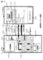
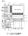
図1には本発明に係るデータプロセッサの一実施例であるCPUと本発明に係る周辺回路の一実施例であるメモリとが接続された状態で示される。 FIG. 1 shows a state in which a CPU as an embodiment of a data processor according to the present invention and a memory as an embodiment of a peripheral circuit according to the present invention are connected.
同図に示されるメモリ1は、代表的に示されたメモリセルアレイ100とアクセスサイクル制御部101を一つの半導体基板に備え、データプロセッサ2からのアクセス要求(200,201,202)に対して自ら内蔵する自励発振回路102の発振出力に同期して当該アクセス要求に従ったリード動作又はライト動作を行うと共に、その内部動作に同期して上記データプロセッサ2に上記アクセス要求に対する応答要求(103)を出力する。
The
同図に示されるCPU2は、代表的に示された演算回路204、演算回路204に一方のポートが結合されたバッファメモリ206、バッファメモリ206の他方のポートと外部のデータバス211とに結合された入出力バッファ回路205、外部のメモリ1やその他図示しない周辺回路にアクセス要求などを行うアクセス制御回路207、及び命令実行シーケンス制御回路や割込み制御回路など中央処理装置全体の動作を制御する中央制御部208を一つの半導体基板に備え、メモリ1などの所要の周辺回路に対してアクセス要求(200、201、202)を行うと共に、アクセス要求を行った周辺回路例えばメモリ1からの応答要求(103)を受け、これに同期して当該アクセス要求の種別に応じ外部からバッファメモリ206にデータを取り込み又はバッファメモリ206から外部にデータを出力する。上記メモリ1はそれ固有の内蔵自励発振回路102の発振出力に同期して動作される。その一方においてCPU2はシステムの動作クロックに209に同期し動作される。
The
CPU2がメモリ1に対してアクセスを行う場合、アクセスの開始をメモリ1にアクセススタート信号200によって伝える。アクセススタート信号200はメモリにとってチップ選択信号と等価な信号とみなされる。特に制限されないが、本実施例に従えば、アクセス制御回路207はチップ選択コントローラとしての機能を内蔵する。この機能は、CPU2から外部に出力されるアドレス信号の上位数ビットをデコードしてチップ選択信号を形成するデコーダに置き換えることができる。何れの場合においても、アクセス対象とすべき周辺回路に割当てられたアドレスとCPU2で生成されるアドレスを参照するものであり、この意味において、メモリなどの周辺回路へのアクセス要求特にアクセス開始の指示は、アクセスアドレスを生成する回路部分が直接的又は間接的に行うものであり、アクセス制御回路はそのような回路部分を含めたものとして把握される。
When the
データ転送の方向はリード/ライト信号201によって指示される。リードとは、メモリ1などの周辺回路からCPU2へのデータ転送であり、ライトとは、CPU2からメモリ1などの周辺回路へのデータ転送である。本実施例に従えば、アクセスが要求された周辺回路内のデータの位置指定(ポインタ)はアドレスバス210に供給されるアドレス信号で指定される。データ転送語数はシングルモード/バーストモードの指示信号(シングル/バースト信号)202によって指示される。連続データ転送モードであるバーストモードを有しないものにあってはシングル/バースト信号202は不要である。
方向 The direction of data transfer is specified by the read /
アクセスサイクル制御部101は、アクセススタート信号200によってアクセス要求を検出すると、これに応答して内部動作のアクセスサイクル信号を自励発振回路102の発振出力に基づいて生成する。メモリ1の内部ではリード/ライト制御信号201によって指示されたリードまたはライト動作が上記アクセスサイクル信号に同期して行われる。さらに、メモリ1の外部に対しては、上記アクセスサイクル信号をアクセスクロック信号103としてCPU2に出力する。このアクセスクロック信号103はメモリ1にとって固有のクロック信号であり、これがCPU2からのアクセス要求に対する応答要求としてCPU2に与えられる。
When the access
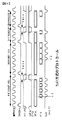
図2にはリード動作におけるメモリ1のデータ出力及びライト動作におけるCPU2のデータ出力タイミングとアクセスクロック信号103との関係が示される。図2に従えば、リード動作が指示されたメモリ1は、アクセスクロック信号103(メモリ内部においてはアクセスサイクル信号)の立ち上がりエッジに対してセットアップタイム(Trs)/ホールドタイム(Trh)を保証するタイミングを以って、所望のデータをデータバス211に出力する。CPU2はそのデータを、アクセスクロック信号103の立上がりタイミングでバッファメモリ206に取り込む。ライトにおいては、CPU2はアクセスクロック信号103の立ち下がり対してセットアップタイム(Tws)/ホールドタイム(Twh)を保証するようバッファメモリ206からデータバス211に出力する。メモリ1はそのデータを上記アクセスサイクル信号の立ち下がりタイミングで取り込む。尚、ライト動作においてもアクセスクロック信号103の立ち上がりを基準にすることもできる。
FIG. 2 shows the relationship between the data output timing of the
図1の実施例に従えば、アクセスサイクル制御部101はバーストモードにおける連続データ転送の完了をCPU2に通知するサイクルコンプリート信号104を出力する。アクセス制御部101はアクセスクロック信号103と等価なアクセスサイクル信号によって転送語数をバーストカウンタ105で計数し、カウントアップの状態をサイクルコンプリート信号104として出力する。サイクルコンプリート信号104に代えてそれと同一の機能をCPU2側に実現してもよい。即ち、CPU2側にアクセスクロック信号103を計数するバーストカウンタを設ければよい。
According to the embodiment of FIG. 1, the access
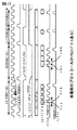
図3には上記実施例の比較例としてウェイトステート制御部を介してデータ転送を可能にするシステムのブロック図が示され、図4にはそのデータ転送タイミングが示される。 FIG. 3 is a block diagram of a system which enables data transfer via a wait state control unit as a comparative example of the above embodiment, and FIG. 4 shows the data transfer timing.
図3においてCPU400が外部のメモリ401に対してデータ転送を行う場合、データ転送の開始がメモリ401とウェイトステート制御部402にアクセススタート信号403で通知される。アクセススタート信号403を受け取ったメモリ401は、リード/ライト制御回路404にてリード/ライト信号405に従ってリードまたはライト動作を開始する。これに同期して上記ウェイトステート制御部402もアクセススタート信号403及びリード/ライト信号405などを解釈して、CPU400と同一の動作クロック406を基にアクセス完了を示すためのウェイト信号407を発生すべく、ウェイトカウンタ408の計数を開始する。リード動作においてメモリ401はその製造/販売業者が保証する時間を経過することによってリードされるべきデータをデータバス409に出力することができる。また、ライト動作においてメモリ401はその製造/販売業者が保証する時間を経過することによってCPU400が出力したデータバス409上のデータを内部に取り込むことができる。上記製造/販売業者が保証する時間を経過したことによるリード動作又はライト動作の完了は、ウェイトステート制御部402からCPU400にウェイト信号407の偽(False)への変化を以って、通常はCPUの動作クロック406に同期して伝えられる(ウェイト信号が非同期信号の場合はCPU側でその動作クロックに同期してウェイト信号を確認する)。例えば図4において、リード動作で時刻t1にウェイト信号が偽(ローレベル)にされると、CPUはデータバス上のデータを読み込む。ライト動作において時刻t2にウェイト信号が偽にされると、CPUはライトすべきデータがメモリに取り込まれたことを確認して当該ライトデータの出力を止める。
In FIG. 3, when the
図4のタイミングから明らかなように、リードサイクルとライトサイクルでは、通常、ウェイト信号を偽にする位置(タイミング)が異なる。また、バーストモードにおいてウェイト信号は、転送語数分連続してサイクリックに発生されるべきであることは当然であるが、第一語目の発生間隔と第二語目以降の発生間隔が異なる。このため、ウェイト信号407の変化をCPU400が確認すると、CPU400は一連のリードまたはライトサイクルを完了し、次のサイクル開始までアクセス制御回路410を待機させる。また、同一動作モードにおけるリードサイクルとライトサイクルの切換え時には、図4のTdisで示されるよな切換え時間が必要とされる。これはクロックにて同期してウェイト信号を確認しているためである。このように、ウェイト信号を利用するデータ転送の場合には複雑な制御と余計な時間を費やさなければならない。
(4) As is clear from the timing in FIG. 4, the position (timing) at which the wait signal is made false usually differs between the read cycle and the write cycle. In the burst mode, the wait signal should be generated cyclically continuously for the number of transfer words, but the generation interval of the first word is different from the generation interval of the second and subsequent words. Therefore, when the
上記実施の形態によれば以下の作用効果が有る。 According to the above embodiment, the following operation and effect can be obtained.
(1)図1及び図2に示される本実施例においては、リードサイクルとライトサイクルでは、通常、メモリなどの周辺回路が発生するアクセスサイクルの発生開始位置ならびにその変化の更新タイミングが異なるが、CPU2はこれらの複雑なタイミングを考慮することなくアクセスクロック信号103の変化に従ってデータの入出力だけに専念すればよい。すなわち、従来必要とされたウェイトステート制御部無しでも複雑なタイミングでのデータ転送が実現できる。このことは、もちろんシングル転送とバースト転送の両方に適応している。
(1) In the present embodiment shown in FIGS. 1 and 2, the read cycle and the write cycle usually differ in the start position of the access cycle generated by the peripheral circuit such as the memory and the update timing of the change. The
(2)ウェイトステート制御部を無くし、メモリなどの周辺回路から出力されるアクセスクロック信号103でデータ転送を行うので、実質的にアクセスサイクル時間の低減とバス使用効率向上が実現できる。すなわち、メモリなどの周辺回路はそれ固有の内蔵自励発振回路102の発振出力に同期して動作され、当該周辺回路に対してアクセス要求を行うCPUの動作クロック信号209とは非同期で動作され、相互間のデータインタフェースは相互に対等なアクセス要求とそれに対する応答要求によって実現する。したがって、従来CPUなどのデータプロセッサの基本動作クロックの整数倍に限定されていた一連のデータ転送時間を、メモリなどの周辺回路の動作速度などの特性に応じて発生される固有自励発振周波数に依存した応答要求のクロックサイクルに従って決定することができる。これにより、周辺回路及びCPU夫々の特性の限界時間でのデータ転送が容易に実現できる。換言すれば、従来問題とされたCPUの動作クロックとの同期のために発生されていた無駄時間を軽減できる。
{Circle around (2)} Since the wait state control unit is eliminated and data is transferred using the
(3)CPU2は、周辺回路とインタフェースされるバッファメモリ206をオンチップで備えるから、CPU内部ユニット204と外部との間のデータ転送速度の相違を内部で吸収し、アクセス要求によるリードデータやライトデータの処理に対して逐次的な待ち時間が介在されることを防止できる。
(3) Since the
(4)上記実施例によるデータ転送形式は、局所的に考えればメモリにもバス権を持たせたと拡張して考えることもできる。すなわち、データ転送の開始時は、CPU2の動作クロック209でシステムが動作していたものが、データ転送中は、メモリの動作クロック103でシステムが動作していると考えられ、動的にバス権が移動したように見える。この考え方は、将来LSIの集積度が向上し論理機能がメモリにもマージされる時期には特に有効な意味を持つものと考えられる。
(4) The data transfer format according to the above-described embodiment can be extended assuming that the bus is also given to the memory when considered locally. That is, at the start of data transfer, the system was operating at the
図5には上記メモリの一実施例ブロック図が示される。同図に示されるメモリ1は、特に制限されないが、スタティック・ランダム・アクセス・メモリ(SRAM)として、公知の半導体集積回路製造技術によって単結晶シリコンのような1個の半導体基板に形成される。
FIG. 5 is a block diagram showing an embodiment of the memory. Although not particularly limited, the
同図に示されるメモリ1は、ロウアドレス信号の入力端子AR0〜ARm、カラムアドレス信号の入力端子AC0〜ACn、データ入出力端子I/O0〜I/Op、チップ選択信号入力端子CS、アウトプットイネーブル信号入力端子OE、ライトイネーブル信号入力端子WE、アクセスサイクル信号出力端子AC、バースト/シングル切換信号入力端子B/S、そして図示しない電源端子が設けられている。図1との対応で説明すれば、チップ選択信号入力端子CSにはアクセススタート信号200が供給され、アウトプットイネーブル信号入力端子OEにはリード/ライト信号201を構成するリード信号が供給され、ライトイネーブル信号入力端子WEにはリード/ライト信号201を構成するライト信号が供給され、アクセスサイクル信号出力端子ACからは上記アクセスサイクル信号103が出力される。
The
メモリセルアレイ100にはスタティック型メモリセルがマトリクス配置されており、メモリセルの選択端子に結合されたワード線はロウアドレスデコーダ110の出力に結合される。ロウアドレスデコーダ110は外部から供給されるロウアドレス信号を内部相補アドレス信号に変換して出力するロウアドレスバッファ111の出力を受け、これをデコードすることによって、ロウアドレス信号に対応する1本のワード線を選択レベルに駆動する。メモリセルのデータ入出力端子に結合されたビット線はカラムスイッチ回路112を介してコモンデータ線113に共通接続される。コモンデータ線113に導通されるべきビット線の選択はカラムアドレスデコーダ114の出力を受ける上記カラムスイッチ回路112が行う。カラムアドレスデコーダ114は外部から供給されるカラムアドレス信号を内部相補アドレス信号に変換して出力するカラムアドレスバッファ115の出力を受け、これをデコードすることによって、カラムスイッチ回路112によるビット線の選択動作を行う。116はメモリセルからのコモンデータ線113に読出されたデータを増幅して外部に出力するセンスアンプ及び出力バッファ回路であり、その入力はコモンデータ線113に、出力はデータ入出力端子I/O0〜I/Opに結合される。117はデータ入出力端子I/O0〜I/Opに与えられた書込みデータを入力する入力バッファであり、その出力はコモンデータ線113に結合される。118はデータラッチ回路若しくはコモンデータ線のイコライズ又はプリチャージのためのデータコントロール回路である。
(4) Static memory cells are arranged in a matrix in the
アクセス制御部101は、サイクルタイミング発生回路1010と、内部タイミング発生回路1011を備える。内部タイミング発生回路1011は上記入力端子CS,OE,WE,B/Sに結合され、アクセススタートの検出、リード/ライト動作の判定、バーストモード/シングルモードの判定などを行って内部動作モードを決定し、サイクルタイミング発生回路1010から供給されるアクセスサイクル信号に同期してその動作モードに対応した内部動作タイミング信号を生成する。サイクルタイミング発生回路1010はCS端子から与えられるアクセススタートの指示に基づいて上記内部タイミング発生回路1011から与えられる信号に同期して自励発振回路102の発振出力に基づいてサイクルタイミング信号1013及びアクセスクロック信号103を生成する。尚、遅延回路1014は自励発振出力の位相調整用に用いられ、遅延回路1015は外部に出力されたアクセスクロック信号103とサイクルタイミング信号1013との位相合わせ用に用いられる。
The
図6には上記サイクルタイミング発生回路1010の詳細な一例回路が示される。自励発振回路102は、特に制限されないが、2入力型アンドゲート1020と当該アンドゲート1020の出力をその一方の入力に帰還させるインバータアンプ1021から成る帰還ループを有し、その発振及び停止を制御するトリガ回路がアンドゲート1020の他方に入力に接続されて構成される。トリガ回路は、初期状態において出力がハイレベルにされるセレクタ1022の出力が入力されると共にオアゲート1023の出力が帰還入力されるアンドゲート1024を備える。上記オアゲート1023はそのアンドゲート1024の出力と上記内部タイミング発生回路1011からリード或はライト動作の開始に同期して供給されるワンショットパルスのようなトリガ信号1025とを受けて、その出力をアンドゲート1020に供給する。尚、1026〜1028で示されるものは波形整形素子(若しくは遅延素子)である。この自励発振回路102は初期状態においてローレベルを出力する。この状態でトリガ信号1025がワンショットパルスで変化されると、アンドゲート1020とインバータアンプ1021で構成される帰還ループに発振を生ずる。この発振状態はセレクタ1022の出力がローレベルにパルス変化されてオアゲート1023の出力がローレベルにされるまで継続される。
FIG. 6 shows a detailed example circuit of the cycle timing generation circuit 1010. The self-
図6の構成においては、発振の停止を制御するために、バーストカウンタ105及びセレクト1022が利用される。セレクタ1022はB/S信号若しくはそれと等価な内部信号が供給され、シングルモードにおいて波形整形素子1027の出力を選択する。したがって、シングルモードにおいて自励発振回路102はアクセスクロック信号103及びサイクルタイミング信号1013をその1サイクル分変化させて発振動作を停止する。バーストモードではバーストカウンタ105の出力を選択する。バーストカウンタ105は、メモリセルアレイからの連続データ読出し語数を波形整形素子1027の出力パルス変化に基づいて計数し、その計数結果が所定の計数値(目的とするバースト転送語数)に到達する状態を以ってハイレベルからローレベルに変化するワンショットパルスを出力する。したがって、バーストモードにおける連続読出し語数分のアクセスサイクルが発生されると、自励発振回路102の発振動作を停止させる。
In the configuration of FIG. 6, the
図7には図6のメモリの一例動作タイミングチャートが示される。同図に示されるようにリードサイクルにおいて読出しデータが出力されるタイミングに同期してアクセスサイクル信号出力端子ACが変化され、また、ライトサイクルにおいてアクセスサイクル信号出力端子ACが変化されタイミングに同期してCPUから書込みデータが供給される。 FIG. 7 shows an example operation timing chart of the memory of FIG. As shown in the figure, the access cycle signal output terminal AC is changed in synchronization with the timing at which read data is output in a read cycle, and the access cycle signal output terminal AC is changed in synchronization with the timing in a write cycle. Write data is supplied from the CPU.
図8には上記CPU2の詳細な一実施例ブロック図が示される。同図に示されるCPU2は、特に制限されないが、公知の半導体集積回路製造技術によって単結晶シリコンのような1個の半導体基板に形成される。図1と同一の回路ブロックには同一符合を付してその詳細な説明を省略する。ここではバッファメモリ206について詳細に説明する。
FIG. 8 is a block diagram showing a detailed embodiment of the
バッファメモリ206はFIFO(ファーストイン・ファーストアウト)形式のリードバッファ2061、ライトバッファ2062、及びバッファ制御回路2063を有する。リードバッファ2061はCPUによるリード方向にデータ転送専用とされ、ライトバッファ2062はCPUによるライト方向のデータ転送専用とされる。双方のバッファ2061,2062は上記アクセスクロック信号103で与えられるメモリ1からの応答要求に基づいて制御される非同期ポート2064と、内部の動作クロック209に同期して制御される同期ポート2065とを有する。バッファ制御回路2063は非同期ポート2064を制御するための非同期制御部2063Aと、同期ポート2065を制御するための同期制御部2063Bを有する。非同期ポート2064は上記入出力バッファ回路205に結合され、同期ポート2065は演算回路204に含まれるレジスタ群やキャッシュメモリなどにインタフェース可能にされる。
The
非同期制御部2063Aは、アクセスクロック信号103の上記変化に同期してライトバッファ2062にリード動作を指示する非同期リード信号(ASync Read Signal)とそのときの非同期リードアドレス(ASync Read Pointer)を供給し、また、アクセスクロック信号103の上記変化に同期してリードバッファ2061にライト動作を指示する非同期ライト信号(ASync Write Signal)とそのときの非同期ライトアドレス(ASync Write Pointer)を供給する。アクセスクロック信号103の変化に同期してリードバッファ2061をアクセスすべきかライトバッファ2062をアクセスすべきかは、そのアクセスクロック信号103に対応されるCPU2のアクセス要求がリード或はライトの何れであるかを示す情報を中央制御部208から受け取ることによって判定する。
The asynchronous control unit 2063A supplies an asynchronous read signal (ASync Read Signal) for instructing a read operation to the
同期制御部2063Bは、中央制御部208における命令実行制御の一環として動作される。例えばロード命令やストア命令或はムーブ命令のようなデータ転送命令などの実行に伴ってメモリリード動作を必要とするときは、動作クロック209に同期してリードバッファ2061にリード動作を指示する同期リード信号(Sync Read Signal)とそのときの同期リードアドレス(Sync Read Pointer)を供給し、また、データ転送命令などの実行に伴ってメモリライト動作を必要とするときは、動作クロック209に同期してライトバッファ2062にライト動作を指示する同期ライト信号(Sync Write Signal)とそのときの同期ライトアドレス(Sync Write Pointer)を供給する。リードバッファ2061をアクセスすべきかライトバッファ2062をアクセスすべきかは、命令実行に伴って中央制御部208から出力される命令解読信号が与えられることによって決定される。
The synchronization control unit 2063B is operated as a part of the instruction execution control in the
図8の例ではメモリ1は上記サイクルコンプリート信号104の出力機能を有していない。それと同等の機能は非同期制御部2063Aに内蔵されるバーストカウンタ2066が行って、バースト転送サイクル終了をアクセス制御回路207に与える。本実施例のCPU2においてバーストカウンタ2066のカウントアップ信号はリードバッファ2061への書込み完了及びライトバッファ2062からの読出し完了を中央制御部208へ通知することにも利用される。図9に基づいてこれを説明する。
In the example of FIG. 8, the
図9にはバッファ制御回路2063におけるリードバッファ2061に関する回路部分の詳細な一例ブロック図が示される。リードバッファ2061の同期リードアドレスはアップカウンタ2063R1が生成し、リードバッファ2061の非同期ライトアドレスはアップカウンタ2063R2が生成する。アップカウンタ2063R2のアップカウント動作はアクセスクロック信号103がハイレベルに変化され且つ中央制御部208からのリードバッファライト信号が活性化されたタイミングに同期して行われる。アップカウンタ2063R1のアップカウント動作は中央制御部208からのリードバッファリード信号が活性化されると動作クロック209に同期して行われる。双方のアップカウンタ2063R1,2063R2はアンドゲート2063R3のハイレベル出力によって0にクリアされる。クリアされるタイミングはアップカウンタ2063R1の出力値が0でない場合に双方のアップカウンタ2063R1,2063R2の出力が一致されたことが一致検出回路2063R6で検出されたときである。アップカウンタ2063R1の出力値が0であることは、0検出回路2063R4が検出する。アップカウンタ2063R1の出力値が0である場合、0検出回路2063R4による0検出結果はリードバッファ2061の空を意味し、これが中央制御部208に与えられる。中央制御部208は、その状態を検出すると、メモリ1からのリードデータが全て演算回路204に渡ったことを確認できる。図8に示されるバーストカウンタ2066は連続データ転送語数が転送すべき語数に到達したか否かを検出する。到達したことがバーストカウンタ2066によって検出されると、当該バーストカウンタ2066の出力は所定期間ハイレベルに変化される。メモリ1に対するリード動作において上記バーストカウンタ2066の上記ハイレベルへの変化はリード完了を意味する信号としてアンドゲート2063R5に供給される。アンドゲート2063R5は、0検出回路203R6によってアップカウンタ2063R1の出力が0出ないときに上記リード完了を意味する信号を受けると、リードバッファ2061へのリード完了を検出して、これを中央制御部208に渡す。中央制御部208は、リードバッファ2061へのリード完了を検出すると、メモリ1からのリードデータが全てリードバッファ2061に貯えられたことを確認でき、これによって、中央制御部208はリードデータをリードバッファ2061から読出して内部演算処理を即座に開始させることができる。
FIG. 9 is a detailed block diagram showing an example of a circuit portion related to the read buffer 2061 in the
図10にはバッファ制御回路2063におけるライトバッファ2062に関する回路部分の詳細な一例ブロック図が示される。ライトバッファ2062の同期ライトアドレスはアップカウンタ2063W2が生成し、ライトバッファ2062の非同期リードアドレスはアップカウンタ2063W1が生成する。アップカウンタ2063W1のアップカウント動作はアクセスクロック信号103がハイレベルに変化され且つ中央制御部208からのライトバッファリード信号が活性化されたタイミングに同期して行われる。アップカウンタ2063W2のアップカウント動作は中央制御部208からのライトバッファライト信号が活性化されると動作クロック209に同期して行われる。双方のアップカウンタ2063W1,2063W2はアンドゲート2063W3のハイレベル出力によって0にクリアされる。クリアされるタイミングはアップカウンタ2063W1の出力値が0でない場合に双方のアップカウンタ2063W1,2063W2の出力が一致されたことが一致検出回路2063W6で検出されたときである。アップカウンタ2063W1の出力値が0であることは、0検出回路2063W4が検出する。アップカウンタ2063W1の出力値が0である場合、0検出回路2063W4による0検出結果はライトバッファ2062の空を意味し、これによって中央制御部208はライトバッファ2062の空の状態を認識する。メモリ1に対するライト動作において上記バーストカウンタ2066の上記ハイレベルへの変化はライト動作完了を意味する信号としてアンドゲート2063W5に供給される。アンドゲート2063W5は、0検出回路2063W4によってアップカウンタ2063W1の出力が0でないときに上記ライト完了を意味する信号を受けると、ライトバッファ2062へのライト動作完了を検出して、これを中央制御部208に渡す。中央制御部208は、ライトバッファ2062へのライト完了を検出すると、当該メモリライトアクセスに対するメモリからの応答要求に応ずるメモリ1へのライトデータが全てライトバッファ2062から出力されたことを確認できる。
FIG. 10 is a block diagram showing a detailed example of a circuit portion related to the
図11には図8に示されるバッファメモリ206とは別のバッファメモリが示される。同図に示されるバッファメモリ206はリードバッファ2061とライトバッファ2062とに共用されるリード/ライトバッファ2067を有し、バッファ制御回路2063にはそのリード/ライトバッファ2067をリードバッファとして動作させるかライトバッファとして動作させるかの情報が設定されるリード/ライトバッファイネーブルフラグ2068が設けられ、中央制御部208からの指示に従ってその動作が制御される。その他の点は図8と同様であり、それと同一回路ブロックには同一符合を付してその詳細な説明を省略する。これによってチップ面積の低減に寄与する。
FIG. 11 shows a buffer memory different from the
図12には図5のメモリに対して制御パラメータレジスタを有する実施例の要部が示される。すなわち、図6のバーストカウンタ105によって計数すべき連続データ転送語数の目的転送語数(カウントアップする転送語数)をプリセット可能に保持するパラメータレジスタ1051を有する。このパラメータレジスタ1051はCPU2の中央制御部208の制御によってプログラマブルに所望のパラメータ(バースト転送語数を特定する情報)が転送される。その他の構成は図5及び図6と同様であり、それと同一回路ブロックには同一符合を付してその詳細な説明を省略する。これによってデータ転送の自由度若しくはその制御の柔軟性が増す。尚、パラメータレジスタ1051は、バーストカウンタ105がその計数ビット数に応じた記憶段を有する場合、当該記憶段をプリセット可能に構成してこれをパラメータレジスタとすることができる。
FIG. 12 shows a main part of an embodiment having a control parameter register for the memory of FIG. That is, there is provided a parameter register 1051 which holds the number of target transfer words (the number of transfer words to be counted up) of the number of continuous data transfer words to be counted by the
図13にはデータバスのビット数に対して例えば1/2nビットのマルチビット入出力機能を有する相互に同一のメモリをCPU2とインタフェースさせるときの実施例が示される。この実施例においてCPU2は、バッファメモリ206及び入出力バッファ回路205を複数組み備える。例えば、データバス211が32ビットでメモリ1の並列入出力ビット数が16ビットのとき、16ビットの上位側データバス211Uは入出力バッファ回路205Uを介して一方のメモリ1Uに、16ビットの下位側データバス211Uは入出力バッファ回路205Lを介して他方のメモリ1Lに結合される。アクセススタート信号200、リード/ライト信号201、シングル/バースト信号202、アドレスバス210はメモリ1U及び1Lに共通接続される。アクセスクロック信号103Uはバッファメモリ206Uに、アクセスクロック信号103Lはバッファメモリ206Lに夫々各別に接続される。夫々のメモリ1U,1Lから出力されるサイクルコンプリート信号104U,104Lはサイクルコンプリート制御回路2069に供給され、双方のメモリアクセス終了をアクセス制御回路207に伝達する。
FIG. 13 shows an embodiment in which mutually identical memories having a multi-bit input / output function of, for example, 1/2 n bits with respect to the number of bits of the data bus are interfaced with the
実際のメモリの並列入出力ビット数は、×4,×8,×9,×16,×18ビットが主流であり、CPUの並列データ入出力ビット数は、×16,×32,×36,×64,×72ビットなどとされているから、それに対応してメモリとCPUをインタフェースさせるには、図13で示したように、複数ビット毎にバッファメモリを設けることが必要かつ重要になる。 The actual number of parallel input / output bits of the memory is mainly × 4, × 8, × 9, × 16, × 18 bits, and the number of parallel data input / output bits of the CPU is × 16, × 32, × 36, Since it is x64, x72 bits, etc., it is necessary and important to provide a buffer memory for each of a plurality of bits as shown in FIG.
図14には異なる特性/機能を有するメモリを混在させてシステムを構成する場合の実施例が示される。この場合には、細かい端子機能や接続条件を無視すれば、基本的にはアクセスクロックに合わせてデータ転送が可能であるため、メモリ1−1のアクセスクロック信号103−1とメモリ1−2のアクセスクロック信号103−2がCPU2の外部でオア(OR)ゲート300を介してバッファ制御回路2063に結合される。同様に、メモリ1−1のアクセスコンプリート信号104−1とメモリ1−2のアクセスコンプリータ信号104−2もCPU2の外部でオアゲート301を介してアクセス制御回路207に結合される。その他のアクセススタート信号200、リード/ライト信号201、シングル/バースト信号202、アドレスバス210、データバス211などはメモリ1−1,1−2に共通接続される。これによって、異なる特性/機能を有するメモリなどの周辺回路を混在させてシステムを構成することができる。
FIG. 14 shows an embodiment in which a system is configured by mixing memories having different characteristics / functions. In this case, if the fine terminal functions and connection conditions are ignored, data transfer can be basically performed in accordance with the access clock. Therefore, the access clock signal 103-1 of the memory 1-1 and the data of the memory 1-2 are not transmitted. Access clock signal 103-2 is coupled to
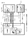
図15には上記実施例で説明したCPU2やメモリ1を用いたデータ処理システムの全体的な一実施例が示される。図15において上記実施例のメモリ(RAM)1と同様のプロトコールでデータ転送可能にされた周辺回路として、メモリ(ROM)3、ハードディスク装置41及びフレキシブルディスク装置42とインタフェースされるファイル制御装置4、フレームバッファ51に対する描画制御及び描画された画像データをモニタ52に表示させる表示制御を行う表示制御装置5、プリンタ61やキーボード62とインタフェースされるパラレル/シリアルポート6、及びコミュニケーション装置10が設けられる。それらの周辺回路は自らの動作特性に応じた固有の自励発振回路102を備えて、上記メモリ同様にCPU2からのアクセス要求に対して応答要求を返すことでデータ転送を実現する。図15において9はシステム監視装置であり、ウォッチドッグタイマによってシステム異常を監視したり電源電圧の状態を監視したりする。高速データ転送装置8は例えばダイレクト・メモリ・アクセス・コントローラのような回路であって、CPU2とのバス権調停はバス権監視装置7が行う。高速データ転送装置もCPU2と同様のデータ転送制御を行う。21はCPU2に固有の外付けキャッシュメモリであり、CPU2の内蔵キャッシュメモリ22に対して2次キャッシュメモリとされる。図15のデータ処理システムは、アドレス及びデータバス11やコントロールバス12が形成された実装基板に構成されている。
FIG. 15 shows an overall embodiment of a data processing system using the
図15のデータ処理システムにおいて、メモリや入出力回路に対するウェイトステート制御を要しないため、そのためのメモリコントローラや入出力コントローラは実装基板上に設けられていない。 In the data processing system of FIG. 15, since a wait state control for a memory and an input / output circuit is not required, a memory controller and an input / output controller for the control are not provided on a mounting board.
以上本発明者によってなされた発明を実施例に基づいて具体的に説明したが、本発明はそれに限定されるものではなく、その要旨を逸脱しない範囲において種々変更可能であることは言うまでもない。 While the invention made by the present inventors has been specifically described based on the embodiments, the present invention is not limited thereto, and it is needless to say that various changes can be made without departing from the scope of the invention.
例えば、上記実施例では周辺回路としてRAMのようなメモリに適用した場合について説明したが、周辺回路はそれに限定されず、図15に示される周辺回路はもとよりそれ以外の各種周辺回路に適用できる。また、そのような周辺回路に適用されるものはCPUやダイレクト・メモリ・アクセス・コントローラに限定されず、マイクロプロセッサ、マイクロコンピュータ、シングルチップマイクロコンピュータ、ディジタル・シグナル・プロセッサなどの各種データプロセッサに適用することができる。 For example, in the above embodiment, the case where the peripheral circuit is applied to a memory such as a RAM has been described. However, the peripheral circuit is not limited to this and can be applied to various peripheral circuits other than the peripheral circuit shown in FIG. In addition, the application to such peripheral circuits is not limited to a CPU or a direct memory access controller, but is applicable to various data processors such as a microprocessor, a microcomputer, a single-chip microcomputer, and a digital signal processor. can do.
また、バッファメモリは上記実施例のような完全ディアルポートバッファに限定されず、ユニポートのバッファメモリを時分割でディアルポートに見せかけて用いることも可能である。また、データプロセッサのチップ面積の観点からはバファメモリの深さ(記憶容量)も重要であるが、あまり機能を落すとバスの速度向上に貢献しなくなるため、この項目に関しては、コストパフォーマンスからのトレードオフを考慮して決定される設計的な事項である。なお、バッファメモリの深さは、1度のデータ転送で扱う語数に限定すること(バースト転送での語数の最大値など)がバッファ制御回路の簡略化に役立つと考えられる。 The buffer memory is not limited to the full dual port buffer as in the above embodiment, and a uniport buffer memory can be used as a dual port in a time sharing manner. Also, the depth (storage capacity) of the buffer memory is important from the viewpoint of the chip area of the data processor, but if the function is reduced too much, it will not contribute to the improvement of the bus speed. It is a design matter determined in consideration of off. It is considered that limiting the depth of the buffer memory to the number of words handled in one data transfer (such as the maximum number of words in burst transfer) is useful for simplifying the buffer control circuit.
1 メモリ
1U,1L メモリ
100 メモリセルアレイ
1−1,1−2 メモリ
101 アクセスサイクル制御部
1010 サイクルタイミング発生回路
1011 内部タイミング発生回路
1013 サイクルタイミング信号
102 自励発振回路
103 アクセスクロック信号
103U,103L アクセスクロック信号
103−1,103−2 アクセスクロック信号
105 バーストカウンタ
1051 パラメータレジスタ
2 CPU
200 アクセススタート信号
204 演算回路
205 入出力バッファ回路
205U,205L 入出力バッファ回路
206 バッファメモリ
206U,206L バッファメモリ
2061 リードバッファ
2062 ライトバッファ
2063 バッファ制御回路
2063A 非同期制御部
2063B 同期制御部
2064 非同期ポート
2065 同期ポート
2066 バーストカウンタ
207 アクセス制御回路
208 中央制御部
209 動作クロック信号
210 アドレスバス
211 データバス
211U,211L データバス
300,301 オアゲート
3 メモリ
4 ファイル制御装置
5 表示制御装置
6 パラレルシリアルポート
10 コミュニケーション装置
200
Claims (5)
上記データプロセッサは、アクセス制御回路と、上記第1メモリに対応する第1バッファ回路と、上記第2メモリに対応する第2バッファ回路と、上記第1メモリから出力される第1サイクルコンプリート信号と上記第2メモリから出力される第2サイクルコンプリート信号とを供給されるサイクルコンプリート制御回路とを有し、
上記第1バッファ回路は上記第1メモリから供給される第1アクセスクロック信号に従って動作し、
上記第2バッファ回路は上記第2メモリから供給される第2アクセスクロック信号に従って動作し、
上記サイクルコンプリート制御回路は、上記第1サイクルコンプリート信号と上記第2サイクルコンプリート信号の双方を受けて、上記第1メモリ及び上記第2メモリ双方のメモリアクセス終了を上記アクセス制御回路に伝達するデータ処理システム。 A data processing system comprising: first and second memories having a first parallel input / output bit number; and a data processor having a second parallel input / output bit number,
The data processor includes an access control circuit, a first buffer circuit corresponding to the first memory, a second buffer circuit corresponding to the second memory, and a first cycle complete signal output from the first memory. A cycle complete control circuit supplied with a second cycle complete signal output from the second memory,
The first buffer circuit operates according to a first access clock signal supplied from the first memory,
The second buffer circuit operates according to a second access clock signal supplied from the second memory,
The cycle complete control circuit receives the first cycle complete signal and the second cycle complete signal, and transmits a memory access end of both the first memory and the second memory to the access control circuit. system.
上記第1及び第2メモリに共通接続されるアドレスバスを有するデータ処理システム。 In claim 1,
A data processing system having an address bus commonly connected to the first and second memories.
上記第1メモリは上位側データバスを介して上記データプロセッサに接続され、上記第2メモリは下位側データバスを介して上記データプロセッサに接続されるデータ処理システム。 In claim 1 or 2,
A data processing system, wherein the first memory is connected to the data processor via an upper data bus, and the second memory is connected to the data processor via a lower data bus.
アクセス制御回路と、
上記第1メモリに対応する第1バッファ回路と、
上記第2メモリに対応する第2バッファ回路と、
上記第1メモリから出力される第1サイクルコンプリート信号と上記第2メモリから出力される第2サイクルコンプリート信号とを供給されるサイクルコンプリート制御回路とを有し、
上記第1バッファ回路は上記第1メモリから供給される第1アクセスクロック信号に従って動作し、
上記第2バッファ回路は上記第2メモリから供給される第2アクセスクロック信号に従って動作し、
上記サイクルコンプリート制御回路は、上記第1サイクルコンプリート信号と上記第2サイクルコンプリート信号の双方を受けて、上記第1メモリ及び上記第2メモリ双方のメモリアクセス終了を上記アクセス制御回路に伝達するデータプロセッサ。 A data processor having a second parallel input / output bit number connected via a data bus to first and second memories having a first parallel input / output bit number,
An access control circuit;
A first buffer circuit corresponding to the first memory;
A second buffer circuit corresponding to the second memory;
A cycle complete control circuit supplied with a first cycle complete signal output from the first memory and a second cycle complete signal output from the second memory;
The first buffer circuit operates according to a first access clock signal supplied from the first memory,
The second buffer circuit operates according to a second access clock signal supplied from the second memory,
A data processor that receives both the first cycle complete signal and the second cycle complete signal and transmits a memory access end of both the first memory and the second memory to the access control circuit; .
Priority Applications (1)
| Application Number | Priority Date | Filing Date | Title |
|---|---|---|---|
| JP2003314902A JP2004046894A (en) | 2003-09-08 | 2003-09-08 | Data processing system and data processor |
Applications Claiming Priority (1)
| Application Number | Priority Date | Filing Date | Title |
|---|---|---|---|
| JP2003314902A JP2004046894A (en) | 2003-09-08 | 2003-09-08 | Data processing system and data processor |
Related Parent Applications (1)
| Application Number | Title | Priority Date | Filing Date |
|---|---|---|---|
| JP02196994A Division JP3490131B2 (en) | 1994-01-21 | 1994-01-21 | Data transfer control method, data processor and data processing system |
Publications (1)
| Publication Number | Publication Date |
|---|---|
| JP2004046894A true JP2004046894A (en) | 2004-02-12 |
Family
ID=31712682
Family Applications (1)
| Application Number | Title | Priority Date | Filing Date |
|---|---|---|---|
| JP2003314902A Pending JP2004046894A (en) | 2003-09-08 | 2003-09-08 | Data processing system and data processor |
Country Status (1)
| Country | Link |
|---|---|
| JP (1) | JP2004046894A (en) |
-
2003
- 2003-09-08 JP JP2003314902A patent/JP2004046894A/en active Pending
Similar Documents
| Publication | Publication Date | Title |
|---|---|---|
| JP3490131B2 (en) | Data transfer control method, data processor and data processing system | |
| US8018784B2 (en) | Semiconductor device and data processor | |
| KR100288177B1 (en) | Memory access control circuit | |
| US8799699B2 (en) | Data processing system | |
| JP3693013B2 (en) | Data processing system, array type processor, data processing apparatus, computer program, information storage medium | |
| JP3328638B2 (en) | Memory device | |
| JP2004118252A (en) | Semiconductor data processing equipment | |
| JP2004029898A (en) | Data processor | |
| JP3708902B2 (en) | Semiconductor device | |
| JP2001312327A (en) | Data processing system provided with controllable clock for partitioned synchronizing interface | |
| JP2004046894A (en) | Data processing system and data processor | |
| JP3861898B2 (en) | Data processing system, array type processor, data processing apparatus, computer program, information storage medium | |
| KR20020012032A (en) | Bus system and command delivering method thereof | |
| US20010005870A1 (en) | External bus control system | |
| JPH04109351A (en) | Dma controller | |
| JP2003099397A (en) | Data processing system | |
| JP2645462B2 (en) | Data processing system | |
| JP2006031227A (en) | Computer system using dma transfer | |
| JP2003233584A (en) | Data transfer device | |
| JP2002073533A (en) | Data processing device | |
| JP2002073534A (en) | Data transfer device | |
| JP2005182312A (en) | Device control circuit | |
| JP2006065444A (en) | Semiconductor integrated circuit and data processor |
Legal Events
| Date | Code | Title | Description |
|---|---|---|---|
| A977 | Report on retrieval |
Free format text: JAPANESE INTERMEDIATE CODE: A971007 Effective date: 20040906 |
|
| A131 | Notification of reasons for refusal |
Free format text: JAPANESE INTERMEDIATE CODE: A131 Effective date: 20041012 |
|
| A521 | Written amendment |
Free format text: JAPANESE INTERMEDIATE CODE: A523 Effective date: 20041213 |
|
| A131 | Notification of reasons for refusal |
Free format text: JAPANESE INTERMEDIATE CODE: A131 Effective date: 20050412 |
|
| A02 | Decision of refusal |
Free format text: JAPANESE INTERMEDIATE CODE: A02 Effective date: 20060207 |