【0001】
【発明の属する技術分野】
本発明は、液晶表示装置やプラズマディスプレイ装置エレクトロルミネッセンス(EL)表示装置等のカラー表示装置における画素領域での欠陥の自動分類方法および自動分類装置に関するものである。
【0002】
【従来の技術】
液晶表示装置に代表されるカラー表示装置は、パーソナルコンピュータなどの表示装置として従来のカラーブラウン管と同等の表示品質が得られる一方、機器の省スペース化に大きく寄与することから、その需要が急速に拡大している。市場ニーズとしては、大画面化、高精細化、低消費電力化が強く、製造プロセス面では、高品質の製品を歩留り良く製造するための品質管理が重要性を増している。
【0003】
基板製造工程は成膜とフォトリソグラフによる金属膜のパターン形成で行なわれる工程が多く、半導体素子の製造工程に類似している。
【0004】
このように製造工程は複雑であり、パターンは微細化する一方、基板は大型化しているため、全画素を無欠陥で作製するのは容易ではない。
【0005】
このため、例えば特許文献1に記載されているような欠陥検査装置で検出された欠陥の画素は、顕微鏡観察や顕微鏡画像の目視観察によって、発生工程や種類別に分類され、品質管理情報として前工程に流されている。
【0006】
【特許文献1】
特開2000−338000号公報
【特許文献2】
特開平6−46428号公報
【0007】
【発明が解決しようとする課題】
しかしながら、従来の分類方法や装置では、欠陥の色、形状、大きさ、発生箇所などが一定していないため、判定に個人差が発生しやすく、分類に熟練を要したり、判定に時間を要するなどの問題があった。このため、観察はもっぱら落射照明によるところが多く、欠陥の種類も限定されていた。
【0008】
以上のような状況により、精度の高いデータを大量に採取することが難しいため、欠陥の発生工程特定や原因究明が迅速に行なえない可能性があるという問題があった。
【0009】
本発明はこのような問題点に鑑みなされたものであり、カラー表示装置の欠陥分類において、欠陥の発生工程や種類を精度良く、かつ短時間に自動分類する方法およびその装置を提供することを目的とする。
【0010】
【課題を解決するための手段】
本発明は、上記目的を達成するために、本発明では、透明基板上にカラー表示画素領域が形成されたカラー表示装置の欠陥分類方法において、予め抽出した欠陥画素を落射照明し該落射照明による前記透明基板からの反射光を検出して落射照明画像を取得する工程と、前記予め抽出した欠陥画素の近傍の無欠陥画素を含む領域を落射照明し該落射照明による前記透明基板からの反射光を検出して落射照明画像を取得する工程と、前記取得した欠陥画素の落射照明画像と前記欠陥画素の近傍の無欠陥画素の落射照明画像とのパターンマッチングを行う工程と、該パターンマッチングをした前記欠陥画素の落射照明画像と前記欠陥画素の近傍の無欠陥画素の落射照明画像との差画像を求める工程と、該差画像から欠陥候補を抽出する工程と、該抽出した欠陥候補を分類する工程とを含むようにした。
また、上記目的を達成するために、本発明では、透明基板上にカラー表示画素領域が形成されたカラー表示装置の欠陥分類方法において、予め抽出した欠陥画素を落射照明し該落射照明による前記透明基板からの反射光を検出して落射照明画像を取得する工程と、前記予め抽出した欠陥画素を透過照明し該透過照明による前記透明基板を透過した光を検出して透過照明画像を取得する工程と、前記予め抽出した欠陥画素の近傍の無欠陥画素を含む領域を落射照明し該落射照明による前記透明基板からの反射光を検出して落射照明画像を取得する工程と、前記予め抽出した欠陥画素の近傍の無欠陥画素を含む領域を透過照明し該透過照明による前記透明基板を透過した光を検出して透過照明画像を取得する工程と、前記取得した予め抽出した欠陥画素の前記落射照明画像と前記透過照明画像と前記予め抽出した欠陥画素の近傍の無欠陥画素を含む領域の前記前記落射照明画像と前記透過照明画像とを用いて欠陥候補を抽出し、該抽出した欠陥候補を分類するようにした。
さらに、上記目的を達成するために、本発明では、透明基板上にカラー表示画素領域が形成されたカラー表示装置の欠陥分類装置を、被検査基板を保持して平面内で移動可能な基板保持手段と、落射照明部と透過照明部とを含む照明系とデータ転送の可能な撮像系とを備えた撮像手段と、前記落射照明部による照明と透過照明部による照明とを交互に切替える切替手段と、前記撮像系から欠陥画素の画像および該欠陥画素の表示色と同一の色を有する近傍の無欠陥画素の画像を入力する手段、パターンマッチング、差分、2値化の画像処理と比較判定をおこなう演算処理手段、画像データや画像処理パラメータの記憶手段、品種情報や画像処理パラメータの入力手段、分類結果を表示する出力手段を備えて構成した。
【0011】
【発明の実施の形態】
以下、本発明の実施形態を図面を参照しながら説明する。
【0012】
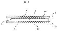
欠陥を分類する対象として、液晶表示装置を例に説明する。液晶表示装置の概略の構成は、図9に示すとおり、スイッチング素子(図示せず)に接続された画素電極19がガラス基板120の上に形成されたTFTアレイ基板20と、着色層21と対向電極22とがガラス基板123の上に形成されたカラーフィルタ基板23との間に、液晶層24を挟持した構成になっている。
【0013】
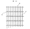
TFTアレイ基板20は、図10に示すように、ガラス基板123の上に、走査信号線25と映像信号線26が格子状に配線され、画素領域27が形成されている。
さて、欠陥の種類には大きく分けて、TFTアレイ基板上の金属膜や半導体膜の残渣(以下、表層異物と呼ぶ)と、TFTアレイ基板とカラーフィルタ基板の間に存在する異物(以下、内層異物と呼ぶ)と、電極パターンの欠損(以下、パターン欠損と呼ぶ)とがある。表層異物は反射率が高いため、観察方向から照明すれば明瞭に観察できるが、基板間の異物はコントラストが低く、判別しずらいのが特徴である。
【0014】
図1に、本発明の実施形態に係る欠陥の抽出および分類をおこなう手順を示す。本発明では、まずTFTアレイ基板を落射照明してTFTアレイ基板からの反射光によるTFTアレイ基板の光学像を検出し、この反射光の光学像を検出して得た画像を処理して欠陥の抽出と分類をおこない、判別できなかった場合もしくは分類が特定されなかった場合には、透過照明によりTFTアレイ基板を透過した光による画像の欠陥の抽出と分類をおこなうものである。
【0015】
落射照明画像による方法は、まず第1工程(図1の1)では、前記した特許文献1に記載されているような方法により予め抽出した所定の位置範囲内にある欠陥画素を落射照明により撮像して得た落射照明画像と、この欠陥画素の表示色と同一の色を有する数画素程度の離れた無欠陥画素領域を撮像して得た参照画像、すなわち落射照明参照画像の2つの画像を入力する。
【0016】
第2工程(図1の2)は落射照明参照画像から画素領域を完全に含む切り出し画像を抜き出し、落射照明検査画像と正規化相互相関法等により画像マッチングをおこない、最も相関係数の高い位置を求めるものである。
【0017】
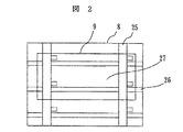
図2は落射照明参照画像8の例で、図3は図2の矩形部9から切り出した切り出し画像10の例である。
【0018】
次の第3工程(図1の3)では、マッチング位置で落射照明参照画像と落射照明検査画像との差の絶対値を求め、予め設定されたしきい値で2値化をおこない、2値化部分に相当する箇所を落射照明検査画像から抜き出し欠陥候補を抽出する。前記落射照明参照画像を欠陥画素の表示色と同一の色を有する近傍の画素領域の画像としたのは、画素領域の一部にカラーフィルタなどの表示色を有する箇所がある場合があり、明るさの差によっては欠陥として誤って抽出されるためである。
【0019】
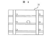
図4に示す表層異物の落射照明検査画像11の例では、表層異物の差画像の2値化画像12は、適切なしきい値により、図5に示すようになり、表層異物欠陥候補の抜き出し部13が選定できたことになる。
【0020】
第4工程(図1の4)では、欠陥の有無を調べ、欠陥候補の位置がパターン領域かあるいはそれ領域外かを判別する。
【0021】
パターン領域は前記切り出し画像の予め設定されたしきい値で2値化された切り出し2値化画像の前記マッチング位置における領域とする。
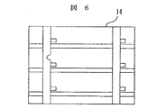
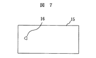
図6に示すようなパターン欠損画像14を例にとると、参照画像との差画像の2値化画像15は図7のようになり、パターン欠損部16は図8に示す前記切り出し画像10の切り出し2値化画像17の2値化パターン部分18に含まれるため、パターン欠損として分類される。
【0022】
前記パターン領域外であれば、欠陥の外観を判定する第5工程(図1の5)に進む。外観とは、明るさや面積や形状などの単体の形態上の特徴をさす。しきい値以上のものは表層異物として第6工程(図1の6)で分類欠陥が出力される。複数のしきい値を設定すれば、異物を細分化することができる。しきい値以下の欠陥候補は透過照明画像を用いてさらに検査がおこなわれる。これは、しきい値以下の特徴の低い欠陥候補は反射性の欠陥ではなく、内層異物の可能性が高いためである。
【0023】
透過照明画像を用いた分類方法は、落射照明に代わり、第7工程(図1の7)で透過照明をおこない撮像した透過照明検査画像と該欠陥画素の表示色と同一の色を有する近傍の無欠陥画素領域の参照画像、すなわち透過照明参照画像とを入力し、落射照明画像の方法と同様の工程で分類をおこなう。
【0024】
ただし、欠陥の外観を判定する第5工程では、明るさのしきい値を欠陥画素の表示色別に設定することが異なる。これは、表示色によって同じ異物でも明るさが異なるためである。
【0025】
欠陥抽出方法は、以上の説明では検査画像と参照画像とのマッチングで欠陥を抽出する方法を説明したが、透過照明画像での分類工程では透過照明検査画像のみを用い、それを2値化しておこなう方法でも可能である。
【0026】
図11は本発明の実施形態に係る液晶表示装置を対象とした欠陥自動分類装置の構成を示すブロック図である。2次元に移動可能なテーブル30にTFTアレイ基板面を上にして保持された被検査基板31の上に撮像顕微鏡を構成する対物レンズ32とチューブレンズ33とCCDカメラ34が設けられ、落射照明装置35からの照明光は顕微鏡光軸に45度だけ傾斜して設置されたハーフミラー36によって被検査基板31を照射するようになっている。テーブル30の下には透過照明装置37が顕微鏡光軸上に配せられている。38は落射照明を遮断する遮光装置で、39は透過照明を遮断する遮光装置である。
【0027】
40a、40bは偏光フィルタで被検査基板両側にクロスニコルの状態で設置されている。41はテーブルの位置制御装置で、42は遮光部の切換え制御装置である。CCDカメラ34は画像入力装置43に接続されている。演算処理部は演算処理装置44と記憶装置45と、入力装置46と、出力装置47とから構成されている。なお、本実施例では分類装置単独の構成を示したが、欠陥修正装置や点灯検査装置の一部であってもよい。
【0028】
テーブル30に搭載固定された被検査基板31は、落射照明参照画像を撮像するため、予め位置のわかった欠陥画素の位置から表示色と同一の色を有する数画素程度離れた無欠陥画素領域に移動する。この時、透過照明の遮光装置39は遮光状態にある。次に、落射照明の遮光装置38を遮光し、透過照明の遮光装置を開放状態にし、無欠陥画素領域の透過照明参照画像を撮像する。次に、テーブルを欠陥画素領域に移動させ、欠陥画素領域の透過照明検査画像を撮像し、遮光装置39を遮光するとともに遮光装置38を開放し、欠陥画素領域の落射照明検査画像を撮像する。
【0029】
以上の4種類の画像データは画像入力装置43を介して記憶装置45に記憶される。演算処理装置44は記憶装置45に記憶された処理プログラムと被検査基板の品種に対応した画像処理パラメータにより2つの落射照明画像のパターンマッチング、差画像の2値化による欠陥候補抽出、欠陥位置判定、欠陥外観判定をおこない、特徴が低く所定の分類がなされなかった場合には引き続き透過照明画像を記憶装置45から読込み、同様の工程をおこない、分類結果を出力装置47に表示する。欠陥修正装置の一部に組込まれた装置においては、良否判定や修正処理判定の情報を出力することも可能である。
【0030】
また、情報ネットワークへ画像データや分類結果情報を転送することもできる。被検査基板の製造工程来歴情報を利用すれば、欠陥発生頻度の時系列変化や多面取り基板での欠陥座標解析、さらにプロセス装置別といった時間、空間、装置、プロセスなど多次元での分析が可能になり、前工程での有用な品質管理情報となる。
【0031】
【発明の効果】
以上のように、本発明による欠陥自動分類方法によれば、欠陥画素と同一表示色の無欠陥画素との比較処理をおこなうため、欠陥部分を精度良く抽出でき、配線パターン領域とパターンに囲まれた領域別に欠陥が分離識別できる。また、欠陥候補を表示色別に設定した明るさしきい値で判別するため、欠陥の種類や発生工程を特定できる自動分類方法を提供することができる。
また、落射照明画像と透過照明画像を併用して分類するため、落射照明画像では判別が難しかった欠陥を透過照明で検査するため、基板間の異物も抽出、分類することが可能となる。
【0032】
本発明による欠陥自動分類装置によれば、欠陥の発生工程や種類を精度良く、しかも短時間に自動分類できるため、多品種で大量の基板に適用でき、有用な品質管理情報を提供することができる。
【図面の簡単な説明】
【図1】本発明の一実施例による欠陥の自動分類方法を示す図。
【図2】落射照明参照画像の例を示した図。
【図3】落射照明参照画像からの切り出し画像の例を示した図。
【図4】表層異物の落射照明検査画像の例を示した図
【図5】表層異物の画像と切り出し画像とのマッチング状態での差画像の2値化画像の図。
【図6】パターン欠損画像の例を示した図。
【図7】パターン欠損画像と切り出し画像とのマッチング状態での差画像の2値化画像の図。
【図8】切り出し画像の2値化画像の例を示した図。
【図9】液晶表示装置の概略の構成を示した図。
【図10】TFTアレイ基板の概略の構成を示した図。
【図11】本発明の実施形態に係る液晶表示装置を対象とした欠陥自動分類装置の構成を示すブロック図。
【符号の説明】
1・・・落射照明検査画像と落射照明参照画像の入力工程 2・・・落射照明検査画像と落射照明参照画像の切り出し画像とのマッチング工程
3・・・差画像から欠陥候補を抽出する工程 4・・・欠陥候補の位置を判定する工程 5・・・欠陥候補の外観を判定する工程 6・・・分類結果を出力する工程 7・・・透過照明検査画像と透過照明参照画像の入力工程
13・・・表層異物欠陥候補の抜き出し部 16・・・パターン欠損部 20・・・TFTアレイ基板 30・・・テーブル 31・・・被検査基板
32・・・対物レンズ 33・・・チューブレンズ 34・・・CCDカメラ 35・・・落射照明装置 37・・・透過照明装置 38・・・落射照明を遮断する遮光装置 39・・・透過照明を遮断する遮光装置 40a、40b・・・偏光フィルタ 42・・・遮光装置の切換え制御装置 43・・・画像入力装置 44・・・演算処理装置 45・・・記憶装置 46・・・入力装置 47・・・出力装置[0001]
TECHNICAL FIELD OF THE INVENTION
The present invention relates to a method and an apparatus for automatically classifying defects in a pixel region in a color display device such as a liquid crystal display device or a plasma display device or an electroluminescence (EL) display device.
[0002]
[Prior art]
A color display device represented by a liquid crystal display device provides display quality equivalent to that of a conventional color cathode-ray tube as a display device for a personal computer or the like, but also greatly contributes to space saving of the device. Is expanding. As market needs, large screens, high definition, and low power consumption are strong, and in the manufacturing process, quality control for manufacturing high quality products with high yield is becoming increasingly important.
[0003]
In many cases, the substrate manufacturing process is performed by film formation and pattern formation of a metal film by photolithography, and is similar to the semiconductor device manufacturing process.
[0004]
As described above, the manufacturing process is complicated and the pattern is miniaturized, while the size of the substrate is large. Therefore, it is not easy to manufacture all pixels without defects.
[0005]
For this reason, for example, pixels of a defect detected by a defect inspection apparatus as described in Patent Document 1 are classified by generation process and type by microscopic observation or visual observation of a microscopic image, and are classified as pre-processes as quality control information. Has been washed away.
[0006]
[Patent Document 1]
Japanese Patent Application Laid-Open No. 2000-338000 [Patent Document 2]
JP-A-6-46428 [0007]
[Problems to be solved by the invention]
However, in the conventional classification method and apparatus, since the color, shape, size, occurrence location, and the like of the defect are not constant, individual differences are likely to occur in the determination, and skill is required for the classification, and time is required for the determination. There were problems such as cost. For this reason, observations were mostly made by epi-illumination, and the types of defects were limited.
[0008]
Under the circumstances described above, it is difficult to collect a large amount of high-precision data, so that there is a problem that it is not possible to quickly identify the process of generating the defect or to find the cause.
[0009]
The present invention has been made in view of such a problem, and provides a method and an apparatus for automatically classifying a defect generation process and type with high accuracy in a short time in a defect classification of a color display device. Aim.
[0010]
[Means for Solving the Problems]
In order to achieve the above object, according to the present invention, in a defect classification method for a color display device in which a color display pixel region is formed on a transparent substrate, epi-illumination of defective pixels extracted in advance is performed by the epi-illumination. Detecting reflected light from the transparent substrate to obtain an epi-illumination image, and epi-illuminating a region including non-defective pixels in the vicinity of the previously extracted defective pixel, and reflecting light from the transparent substrate by the epi-illumination. Detecting the epi-illumination image, and performing pattern matching between the epi-illumination image of the acquired defective pixel and the epi-illumination image of a non-defective pixel in the vicinity of the defective pixel, and performing the pattern matching. Obtaining a difference image between the epi-illumination image of the defective pixel and the epi-illumination image of a non-defective pixel in the vicinity of the defective pixel; extracting a defect candidate from the difference image; And to include a step of classifying the defect candidates.
To achieve the above object, according to the present invention, in a defect classification method for a color display device in which a color display pixel region is formed on a transparent substrate, the defective pixel extracted in advance is illuminated by epi-illumination and the transparent pixel is illuminated by the epi-illumination. A step of detecting reflected light from the substrate to obtain an epi-illumination image, and a step of transmitting and illuminating the defective pixel extracted in advance and detecting light transmitted through the transparent substrate by the transmitted illumination to obtain a transmitted illumination image. And epi-illuminating a region including non-defective pixels in the vicinity of the previously extracted defective pixel, and detecting reflected light from the transparent substrate due to the epi-illumination to obtain an epi-illumination image; Transmitting and illuminating an area including a non-defective pixel in the vicinity of the pixel, detecting light transmitted through the transparent substrate by the transmitted illumination, and acquiring a transmitted illumination image; A defect candidate is extracted using the epi-illumination image and the transmitted illumination image of a pixel, and the epi-illumination image and the transmitted illumination image of a region including non-defective pixels in the vicinity of the previously extracted defective pixel. Defect candidates are classified.
Further, in order to achieve the above object, according to the present invention, a defect classification device for a color display device in which a color display pixel region is formed on a transparent substrate is provided. Means, an image pickup means having an illumination system including an epi-illumination section and a transmission illumination section, and an imaging system capable of data transfer, and a switching means for alternately switching between illumination by the epi-illumination section and illumination by the transmission illumination section. Means for inputting an image of a defective pixel and an image of a neighboring non-defective pixel having the same color as the display color of the defective pixel from the imaging system, and performing pattern matching, difference, binarization image processing and comparison determination It is provided with an arithmetic processing means for performing, a storage means for image data and image processing parameters, an input means for type information and image processing parameters, and an output means for displaying a classification result.
[0011]
BEST MODE FOR CARRYING OUT THE INVENTION
Hereinafter, embodiments of the present invention will be described with reference to the drawings.
[0012]
As a target for classifying defects, a liquid crystal display device will be described as an example. As shown in FIG. 9, the schematic configuration of the liquid crystal display device includes a TFT array substrate 20 in which a pixel electrode 19 connected to a switching element (not shown) is formed on a glass substrate 120, and a color layer 21. The liquid crystal layer 24 is sandwiched between the electrode 22 and a color filter substrate 23 formed on a glass substrate 123.
[0013]
In the TFT array substrate 20, as shown in FIG. 10, a scanning signal line 25 and a video signal line 26 are arranged in a grid pattern on a glass substrate 123, and a pixel region 27 is formed.
The types of defects are roughly classified into residues of a metal film or a semiconductor film on a TFT array substrate (hereinafter, referred to as surface foreign matter) and foreign matters (hereinafter, referred to as an inner layer) existing between the TFT array substrate and the color filter substrate. And a defect of the electrode pattern (hereinafter, referred to as a pattern defect). Since surface layer foreign matter has a high reflectance, it can be clearly observed when illuminated from the viewing direction. However, foreign matter between substrates has a low contrast and is difficult to distinguish.
[0014]
FIG. 1 shows a procedure for extracting and classifying defects according to the embodiment of the present invention. In the present invention, first, the TFT array substrate is illuminated by incident light, an optical image of the TFT array substrate is detected by light reflected from the TFT array substrate, and an image obtained by detecting the optical image of the reflected light is processed to detect a defect. The extraction and classification are performed, and if the classification is not performed or the classification is not specified, the image defect is extracted and classified by the light transmitted through the TFT array substrate by the transmitted illumination.
[0015]
In the method using the epi-illumination image, first, in a first step (1 in FIG. 1), a defective pixel within a predetermined position range extracted in advance by the method described in Patent Document 1 is imaged by epi-illumination. And a reference image obtained by imaging a non-defective pixel area separated by about several pixels having the same color as the display color of the defective pixel, that is, an epi-illumination reference image. input.
[0016]
The second step (2 in FIG. 1) is to extract a clipped image completely including the pixel region from the epi-illumination reference image, perform image matching with the epi-illumination inspection image by a normalized cross-correlation method or the like, and determine a position having the highest correlation coefficient. Is what you want.
[0017]
FIG. 2 is an example of the epi-illumination reference image 8, and FIG. 3 is an example of a cut-out image 10 cut out from the rectangular portion 9 in FIG.
[0018]
In the next third step (3 in FIG. 1), the absolute value of the difference between the epi-illumination reference image and the epi-illumination inspection image is determined at the matching position, binarized using a preset threshold, and binarized. A portion corresponding to the converted portion is extracted from the epi-illumination inspection image and a defect candidate is extracted. The epi-illumination reference image is used as an image of a neighboring pixel region having the same color as the display color of the defective pixel because there is a portion having a display color such as a color filter in a part of the pixel region. This is because, depending on the difference in height, a defect is erroneously extracted as a defect.
[0019]
In the example of the incident illumination inspection image 11 of the surface foreign matter shown in FIG. 4, the binarized image 12 of the difference image of the surface foreign matter becomes as shown in FIG. 13 has been selected.
[0020]
In the fourth step (4 in FIG. 1), the presence or absence of a defect is examined to determine whether the position of the defect candidate is in the pattern area or outside the pattern area.
[0021]
The pattern area is an area at the matching position of the cut-out binarized image binarized by a preset threshold value of the cut-out image.
Taking a pattern loss image 14 as shown in FIG. 6 as an example, a binarized image 15 of the difference image from the reference image is as shown in FIG. 7, and a pattern loss portion 16 is the same as that of the cut-out image 10 shown in FIG. Since it is included in the binarized pattern portion 18 of the cut-out binarized image 17, it is classified as a pattern loss.
[0022]
If it is outside the pattern area, the process proceeds to a fifth step (5 in FIG. 1) for determining the appearance of the defect. The term “appearance” refers to features of a single unit such as brightness, area, and shape. Those having a threshold value or more are classified as surface foreign substances, and classified defects are output in the sixth step (6 in FIG. 1). If a plurality of thresholds are set, foreign substances can be subdivided. Defect candidates below the threshold are further inspected using the transmitted illumination image. This is because a defect candidate having a characteristic lower than the threshold value is not a reflective defect but has a high possibility of an inner layer foreign matter.
[0023]
In the classification method using the transmitted illumination image, instead of the epi-illumination, the transmitted illumination inspection image captured by performing the transmitted illumination in the seventh step (7 in FIG. 1) and a nearby image having the same color as the display color of the defective pixel are taken. A reference image of a non-defective pixel area, that is, a transmitted illumination reference image is input, and classification is performed in the same process as that of the epi-illumination image.
[0024]
However, the fifth step of determining the appearance of a defect is different in that a threshold value of brightness is set for each display color of a defective pixel. This is because the brightness differs even for the same foreign matter depending on the display color.
[0025]
In the above description, the method of extracting a defect by matching the inspection image with the reference image has been described in the above description. However, in the classification step of the transmitted illumination image, only the transmitted illumination inspection image is used, and it is binarized. This is also possible.
[0026]
FIG. 11 is a block diagram showing a configuration of an automatic defect classification device for a liquid crystal display device according to an embodiment of the present invention. An objective lens 32, a tube lens 33, and a CCD camera 34, which constitute an imaging microscope, are provided on a substrate 31 to be inspected held on a two-dimensionally movable table 30 with a TFT array substrate surface up. Illumination light from 35 is irradiated on the substrate 31 to be inspected by a half mirror 36 installed at an angle of 45 degrees with respect to the optical axis of the microscope. Below the table 30, a transmission illumination device 37 is arranged on the optical axis of the microscope. Reference numeral 38 denotes a light shielding device for blocking incident illumination, and 39 denotes a light shielding device for blocking transmitted illumination.
[0027]
Reference numerals 40a and 40b denote polarizing filters which are installed on both sides of the substrate to be inspected in a crossed Nicols state. Reference numeral 41 denotes a table position control device, and reference numeral 42 denotes a light-shielding portion switching control device. The CCD camera 34 is connected to the image input device 43. The arithmetic processing unit includes an arithmetic processing device 44, a storage device 45, an input device 46, and an output device 47. In the present embodiment, the configuration of the classification device alone is shown, but it may be a part of a defect repair device or a lighting inspection device.
[0028]
The inspection target substrate 31 mounted and fixed on the table 30 captures an epi-illumination reference image in a non-defective pixel area separated by a few pixels having the same color as the display color from the position of the defective pixel whose position is known in advance. Moving. At this time, the light shielding device 39 of the transmitted illumination is in a light shielding state. Next, the light-shielding device 38 of the epi-illumination is shielded, the light-shielding device of the transmitted illumination is opened, and a transmitted illumination reference image of the non-defective pixel area is captured. Next, the table is moved to the defective pixel area, a transmitted illumination inspection image of the defective pixel area is captured, the light shielding device 39 is shielded and the light shielding device 38 is opened, and an epi-illumination inspection image of the defective pixel area is captured.
[0029]
The above four types of image data are stored in the storage device 45 via the image input device 43. The arithmetic processing unit 44 performs pattern matching of two epi-illumination images, extraction of defect candidates by binarization of a difference image, and defect position determination based on the processing program stored in the storage device 45 and image processing parameters corresponding to the type of the substrate to be inspected. Then, the defect appearance is determined, and if the feature is low and the predetermined classification is not performed, the transmitted illumination image is continuously read from the storage device 45, the same process is performed, and the classification result is displayed on the output device 47. In a device incorporated in a part of the defect repairing device, it is also possible to output information of pass / fail judgment and correction process judgment.
[0030]
Also, image data and classification result information can be transferred to an information network. Utilizing information on the manufacturing process history of inspected substrates, it is possible to analyze time-series changes in the frequency of defect occurrence, defect coordinate analysis on multi-planar substrates, and multidimensional analysis such as time, space, equipment, and process by process equipment. And useful quality control information in the previous process.
[0031]
【The invention's effect】
As described above, according to the defect automatic classification method according to the present invention, since a comparison process is performed between a defective pixel and a non-defective pixel having the same display color, a defective portion can be accurately extracted, and the defective portion is surrounded by the wiring pattern region and the pattern. Defects can be separated and identified for each region. Further, since the defect candidate is determined by the brightness threshold value set for each display color, it is possible to provide an automatic classification method capable of specifying the type of defect and the generation process.
In addition, since the incident illumination image and the transmitted illumination image are classified together, the defect which is difficult to determine in the incident illumination image is inspected by the transmitted illumination, so that the foreign matter between the substrates can be extracted and classified.
[0032]
ADVANTAGE OF THE INVENTION According to the defect automatic classification apparatus by this invention, since the generation | occurrence | production process and the type of a defect can be automatically classified with high precision and in a short time, it can be applied to a large number of substrates of various kinds, and can provide useful quality control information. it can.
[Brief description of the drawings]
FIG. 1 is a diagram showing an automatic defect classification method according to an embodiment of the present invention.
FIG. 2 is a diagram showing an example of an epi-illumination reference image.
FIG. 3 is a diagram showing an example of a clipped image from an epi-illumination reference image.
FIG. 4 is a diagram showing an example of an epi-illumination inspection image of a surface foreign matter; FIG. 5 is a diagram of a binarized image of a difference image in a matching state between the image of the surface foreign matter and the cut-out image;
FIG. 6 is a diagram showing an example of a pattern loss image.
FIG. 7 is a diagram of a binarized image of a difference image in a matching state between a pattern-loss image and a cut-out image.
FIG. 8 is a diagram showing an example of a binarized image of a cut-out image.
FIG. 9 is a diagram illustrating a schematic configuration of a liquid crystal display device.
FIG. 10 is a diagram showing a schematic configuration of a TFT array substrate.
FIG. 11 is a block diagram illustrating a configuration of an automatic defect classification device for a liquid crystal display device according to an embodiment of the present invention.
[Explanation of symbols]
1 ... Inputting of epi-illumination inspection image and epi-illumination reference image 2 ... Matching process of epi-illumination inspection image and cut-out image of epi-illumination reference image 3 ... Step of extracting defect candidate from difference image 4 Step of determining the position of the defect candidate 5 Step of determining the appearance of the defect candidate 6 Step of outputting the classification result 7 Step of inputting the transmitted illumination inspection image and the transmitted illumination reference image 13 ············································································································· ··· CCD camera 35 ··· epi-illumination device 37 ··· transmissive illumination device 38 ··· light-shielding device that blocks epi-illumination 39 • light-shielding device 40a and 40b that blocks transmission illumination · Polarization filter 42 switching control unit 43 ... image input device 44 ... processing unit 45 ... memory 46 ... input device 47 ... output device ... shading device