JP2004120366A - Image processing apparatus and image processing method - Google Patents
Image processing apparatus and image processing method Download PDFInfo
- Publication number
- JP2004120366A JP2004120366A JP2002281145A JP2002281145A JP2004120366A JP 2004120366 A JP2004120366 A JP 2004120366A JP 2002281145 A JP2002281145 A JP 2002281145A JP 2002281145 A JP2002281145 A JP 2002281145A JP 2004120366 A JP2004120366 A JP 2004120366A
- Authority
- JP
- Japan
- Prior art keywords
- value data
- correction value
- bit
- corrected
- bits
- Prior art date
- Legal status (The legal status is an assumption and is not a legal conclusion. Google has not performed a legal analysis and makes no representation as to the accuracy of the status listed.)
- Pending
Links
Images









Landscapes
- Processing Of Color Television Signals (AREA)
- Facsimile Image Signal Circuits (AREA)
- Control Of Indicators Other Than Cathode Ray Tubes (AREA)
- Controls And Circuits For Display Device (AREA)
- Image Processing (AREA)
- Picture Signal Circuits (AREA)
- Transforming Electric Information Into Light Information (AREA)
Abstract
【課題】回路規模を増大することなく、補正を行うことができる画像処理装置、および画像処理方法を提供する。
【解決手段】入力画像信号に基づいて、所定のビット幅の上位ビットを抽出した第1の被補正用ビットに、所定のビット幅に応じた所定のビットだけ大きい第2の被補正用ビットを生成し出力する加算およびオーバフロー処理部421と、ルックアップテーブル(LUT)を記憶するメモリ423と、タイミング調整用のFF422と、FF422から出力された入力信号の下位ビットの被補正用ビットと、メモリ423から出力された2つの補正値データとに基づいて、補間処理を行う補間演算部424とを設ける。
【選択図】 図7An image processing apparatus and an image processing method capable of performing correction without increasing a circuit scale.
A first bit to be corrected, which is obtained by extracting an upper bit of a predetermined bit width based on an input image signal, includes a second bit to be corrected that is larger by a predetermined bit corresponding to the predetermined bit width. An addition and overflow processing unit 421 for generating and outputting, a memory 423 for storing a look-up table (LUT), a FF 422 for timing adjustment, a bit to be corrected as a lower bit of the input signal output from the FF 422, An interpolation calculation unit 424 for performing an interpolation process based on the two correction value data output from the 423 is provided.
[Selection diagram] FIG.
Description
【0001】
【発明の属する技術分野】
本発明は、例えば、画像信号の補正処理を行う画像処理装置、および画像処理方法に関するものである。
【0002】
【従来の技術】
従来、例えば画像処理装置において、画像信号の補正、例えばガンマ補正を行う回路として、デジタル回路を使用した数点の折れ点補正やルックアップテーブル(以下LUT)に基いて補正を行う補正回路が知られている(例えば、特許文献1参照。)。
【0003】
このLUT方式のデジタル方式の補正回路は、補正精度が高いことから、近年では主流になりつつある。
【0004】
【特許文献1】
特開2001−320607号公報
【0005】
【発明が解決しようとする課題】
上述した従来のLUT方式のデジタル方式の補正回路では、入力信号の量子化ビット数をnとすると、2^n個のメモリアドレスを持つメモリをLUTとして使用する。LUTには入力信号レベルに対応するガンマ補正値データを格納し、画像表示装置の印加電圧に対する透過率の特性(V−T特性)を考慮したガンマ補正を行っている。
【0006】
しかし、入力信号レベルを量子化する分解能が増大すればするほど、このLUTに使用するメモリの規模は増大する。
例えば、入力信号レベルの量子化ビット数が10ビットの場合、LUTに使用するメモリに必要な容量は1024word必要となり、入力レベルの量子化ビット数が12ビットの場合は4096word必要となる。
【0007】
このように、1ビット分解能が上がるとメモリ容量は2倍づつ増加する。これに伴い、回路規模は増大し消費電力の増加と共に、メモリに格納するガンマ補正値データの更新時間が増加するという問題があった。
【0008】
本発明は、かかる事情に鑑みてなされたものであり、その目的は、回路規模を増大することなく、補正を行うことができる画像処理装置、および画像処理方法を提供することにある。
【0009】
【課題を解決するための手段】
前記目的を達成するために、第1の発明の画像処理装置は、複数ビットからなる画像信号の補正処理を行う画像処理装置であって、画像信号の内の被補正用ビットをテーブル変換するための補正値データを記憶する記憶手段と、入力画像信号の内の第1の被補正用ビットに基づいて前記記憶手段によりテーブル変換された第1の補正値データ、当該第1の被補正用ビットよりも大きい第2の被補正用ビットに基づいて前記記憶手段によりテーブル変換された第2の補正値データ、および前記入力画像信号から前記被補正用ビットを除いた残りの被補間用ビットに基づいて、補間処理を行い前記入力画像信号に対する第3の補正値データを生成する補間手段とを有する。
【0010】
第1の発明の画像処理装置によれば、複数ビットからなる画像信号の補正処理を行う。
記憶手段では、画像信号の内の被補正用ビットをテーブル変換するための補正値データが記憶されている。
補間手段では、入力画像信号の内の第1の被補正用ビットに基づいて記憶手段によりテーブル変換された第1の補正値データ、当該第1の被補正用ビットよりも大きい第2の被補正用ビットに基づいて記憶手段によりテーブル変換された第2の補正値データ、および入力画像信号から被補正用ビットを除いた残りの被補間用ビットに基づいて、補間処理を行い入力画像信号に対する第3の補正値データが生成される。
【0011】
さらに、前記目的を達成するために、第2の発明の画像処理方法は、複数ビットからなる画像信号の内の被補正用ビットを予め設定した補正値データに基づいてテーブル変換して、当該画像信号の補正処理を行う画像処理装置の画像処理方法であって、入力画像信号の内の第1の被補正用ビットに基づいて前記テーブル変換して第1の補正値データを生成し、当該第1の被補正用ビットよりも大きい第2の被補正用ビットに基づいて前記テーブル変換して第2の補正値データを生成し、当該第1および第2の補正値データ、ならびに前記入力画像信号から前記被補正用ビットを除いた残りの被補間用ビットに基づいて、補間処理を行い前記入力画像信号に対する第3の補正値データを生成する。
【0012】
【発明の実施の形態】
本発明に係る画像処理装置は、画像信号を補正させるルックアップテーブルに基づいて補正値を生成し、その補正値にさらに補間処理を行い、画像信号の補正値を生成する。
以下、本発明に係る画像処理装置の一実施の形態を図を参照しながら説明する。
第1の実施の形態
本発明の第1の実施の形態に係る画像処理装置は、例えば画像信号の入力信号レベルに対し、非線形の光学応答をする液晶等の表示デバイスによる画像処理装置において、ガンマ補正値データを含むルックアップテーブルと、入力された画像信号とルックアップテーブルに基づいて生成された補正値を、直線補正関数により補間する。
より詳細には、画像信号を出力デバイスの特性に合わせるために、必要量より少ないルックアップテーブルと必要量に不足するデータを補間するための補間関数を使用したガンマ補正を行う。
【0013】
以下、本実施の形態に係る画像処理装置の補正回路を採用したLCDパネルを用いたフロント/リアプロジェクタシステムについて説明する。
図1は、本発明に係る画像処理装置の一実施の形態の機能ブロック図である。画像処理装置1は、図1に示すように、A/DPLL2、スキャンコンバータ(Scan Converter)3、信号処理部4、サンプル/ホールドドライバ(S/H Driver)5、LCDパネル6、および基準クロック(クリスタル:XTL)7を有する。
【0014】
画像処理装置1では、例えば信号処理部4の入出力は12ビット、S/Hドライバ5の入力は12ビット、出力は6ビット、LCDパネル6の入力は12ビットの構成とする。
【0015】
A/DPLL2は、例えば、入力されたアナログビデオ信号をA/D変換処理してデジタル信号を生成し、スキャンコンバータ3に出力する。
【0016】
A/DPLL2は、例えば、アナログビデオ信号R(Red )信号、G(Green )信号、B(Blue)信号、水平同期信号(HSYNC )、および垂直同期信号(VSYNC )に基づいて、A/D変換処理して、例えばデジタル信号として8ビット長のR信号、G信号、およびB信号をスキャンコンバータ3に出力する。
また、A/DPLL2は、水平同期信号(HSYNC )および垂直同期信号(VSYNC )を、スキャンコンバータ3に出力する。
【0017】
スキャンコンバータ3は、A/DPLL2から出力されたデジタル信号に基いて、スケーリングおよびディザリング処理等を行い、12ビットのデジタル信号を生成し、信号処理部4に出力する。
【0018】
スキャンコンバータ3は、例えば、基準クロック(XTL)7から出力された基準クロック信号、A/DPLL2から出力された水平同期信号(HSYNC )および垂直同期信号(VSYNC )に基づいて、A/DPLL2から出力されたデジタル信号の8ビット長のR信号、G信号、およびB信号に、スケーリングおよびディザリング処理等を行い、例えばデジタル信号として12ビット長のR信号、G信号、およびB信号を信号処理部4に出力する。
また、スキャンコンバータ3は、同期信号を信号処理部4に出力する。
【0019】
信号処理部4は、スキャンコンバータ3から出力されたデジタル式の入力信号に基づいて、所定の処理を行い処理結果をS/Hドライバ5に出力する。
【0020】
信号処理部4は、例えば、基準クロック(XTL)7から出力された基準クロック、およびスキャンコンバータ3から出力された同期信号に同期して、スキャンコンバータ3から出力された12ビット長のR信号、G信号、およびB信号に基づいて、例えば後述するガンマ補正処理を含む所定の処理を行い、12ビット長のR信号、G信号、およびB信号をS/Hドライバ5に出力する。
【0021】
信号処理部4は、S/Hドライバ5に同期信号を出力する。
信号処理部4は、所定の信号、例えば設定信号等をLCDパネル6に出力する。
【0022】
サンプル/ホールド(S/H)ドライバ5は、例えば、信号処理部4から出力された同期信号に同期して、信号処理部4から出力された画像信号を、サンプル/ホールド処理した後、LCDパネル6に出力する。
【0023】
S/Hドライバ5は、例えば複数のS/Hドライバ5−1〜6、具体的には、R信号の垂直および水平それぞれに対応するS/Hドライバ5−1〜2、G信号の垂直および水平それぞれに対応するS/Hドライバ5−3〜4、B信号の垂直および水平それぞれに対応するS/Hドライバ5−5〜6を有する。
【0024】
LCDパネル6は、S/Hドライバ5から出力された信号に応じた画像を表示する。
LCDパネル6は、例えば、複数のLCDパネル6−1〜3を有する。
【0025】
例えば、LCDパネル6−1は、S/Hドライバ5−1,2から出力される6ビット長のR信号、および信号処理部4から出力された所定の信号に応じた画像を表示する。
【0026】
例えば、LCDパネル6−2は、S/Hドライバ5−3,4から出力される6ビット長のG信号、および信号処理部4から出力された所定の信号に応じた画像を表示する。
例えば、LCDパネル6−3は、S/Hドライバ5−5,6から出力される6ビット長のB信号、および信号処理部4から出力された所定の信号に応じた画像を表示する。
【0027】
上述した構成の画像処理装置1の動作を簡単に説明する。
アナログビデオ信号は、A/DPLL(コンバータ)2でA/D変換され、スキャンコンバータ3でスケーリングおよびディザリング処理が行われ、12ビットのデジタルデータとして出力される。
【0028】
このデジタルデータは、信号処理部4に入力され、後述する内部のガンマ補正回路(ブロック)にてLCDパネル6のV−T特性に合わせたガンマ補正処理が行われ出力される。
出力された画像信号は、サンプル/ホールドドライバ5にて、サンプル/ホールド処理した後LCDパネル6に出力され、LCDパネル6により所定の映像が表示される。
【0029】
図2は、LCD(液晶)パネルの印加電圧に対する透過率の特性(V−T特性)を示す図である。
LCD(液晶)パネル6において、その印加電圧に対する透過率の特性(以下V−T特性)は、図2に示すように非線型の特性を有する。例えば、図2は、ノーマリホワイト透過型液晶のV−T特性である。
【0030】
図3は、入力信号レベルに対する理想透過率特性を示す図である。図4は、ガンマ補正カーブを示す図である。
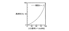
画像処理装置1における表示輝度は、人の階調認識の特性より、例えば図3に示すように入力信号レベルに対し透過率の特性が、指数関数の特性を有することが望まれる。
この2つの特性の条件の要請により、入力信号レベルに対する出力信号レベル(液晶印加電圧)は、図4に示すように非線型の補正を行う必要があり、この補正をガンマ補正と言う。
【0031】
例えば、画像処理装置1で表示された画像を、カメラ等で取り込み、画像処理装置1の出力信号レベルと、信号処理部4の信号レベルとに基づいて、ガンマ補正値データを算出する。この際、本実施の形態に係る画像処理装置1では、入力信号レベル全てのガンマ補正値データをルックアップテーブルとして記憶するのではなく、入力信号が所定の量子化ビットのガンマ補正値データを記憶する。
【0032】
本実施の形態に係る補正回路を含む画像処理装置は、入力信号に基づいて補正を行う場合には、ルックアップテーブルを参照して、入力信号に対応するガンマ補正値データを出力する。また、入力信号のレベルが、ルックアップテーブルにおいて所定の量子化ビットの間隔の間の場合には、入力信号およびルックアップテーブルに基づいて、補間処理を行いガンマ補正値データを出力する。
【0033】
図5は、図1に示した画像処理装置の信号処理部の構成を示す機能ブロック図である。
信号処理部4は、第1の信号処理部41、ガンマ補正回路(ブロック)42、第2の信号処理部43、およびタイミング生成部44とを有する。
【0034】
第1の信号処理部41は、所定の処理、例えばゲイン調整やリミット等の処理を行い、処理結果をガンマ補正回路42に出力する。
例えば、第1の信号処理部41は、R信号を処理する第1の信号処理部41−1、G信号を処理する第1の信号処理部41−2、およびB信号を処理する第1の信号処理部41−3とを有する。
【0035】
ガンマ補正回路42は、第1の信号処理部41から出力された信号に応じて、後述するガンマ補正処理を行い、補正処理結果を第2の信号処理部43に出力する。
例えば、ガンマ補正回路42は、R信号を処理するガンマ補正回路42−1、G信号を処理するガンマ補正回路42−2、およびB信号を処理するガンマ補正回路42−3とを有する。
【0036】
第2の信号処理部43は、ガンマ補正回路42から出力された信号に応じて、所定の処理、例えばゲイン調整やリミットなどの処理を行い、処理結果をS/Hドライバ5に出力する。
例えば、第2の信号処理部43は、R信号を処理する第2の信号処理部43−1、G信号を処理する第2の信号処理部43−2、およびB信号を処理する第2の信号処理部43−3を有する。
【0037】
タイミング生成部44は、水平同期信号(HSYNC)、垂直同期信号(VSYNC)、第1の信号処理部41、ガンマ補正回路42、第2の信号処理部43で処理されたR信号Rout 、G信号Gout 、およびB信号Bout に基づいて、所定のタイミングで制御信号をLCDパネル6に出力する。例えば、この制御信号はLCDパネル6の設定を制御させる。
【0038】
上述した構成の信号処理部4では、R信号Rinが、第1の信号処理部41−1で処理され、ガンマ補正回路42−1で処理され、第2の信号処理部43−1で処理され、処理結果としてR信号Rout が出力される。
【0039】
G信号Ginが、第1の信号処理部41−2で処理され、ガンマ補正回路42−2で処理され、第2の信号処理部43−2で処理され、処理結果としてG信号Gout が出力される。
【0040】
B信号Binが、第1の信号処理部41−3で処理され、ガンマ補正回路42−3で処理され、第2の信号処理部43−3で処理され、処理結果としてB信号Bout が出力される。
【0041】
図6は、図5に示した信号処理部の機能ブロックの一具体例を示す図である。信号処理部4は、例えばより詳細には、図6に示すように、ユーザゲイン411、ユーザブライト412、サブゲイン413、サブブライト414、黒枠415、第1のミュート416、パターンジェネレータ417、OSD418、ガンマ補正回路42、ガンマゲイン431、ガンマブライト432、色むら補正433、ドットライン反転434、第2のミュート435、リミッタ436、ゴーストキャンセル437、および縦筋キャンセル438等の機能ブロックを有する。
【0042】
各機能ブロックを簡単に説明する。なお、各機能ブロックで用いられる係数等のパラメータは、例えば不図示のホストI/Fを介して不図示のホスト装置から設定される。
【0043】
ユーザゲイン411は、例えばユーザコントロールゲイン調整用として乗算処理を行う。ユーザゲイン411の演算は12ビットの入力信号と8ビットの係数とを用いて乗算を行い、所定のビットで四捨五入を行い12ビットのデータをユーザブライト412に出力する。
【0044】
ユーザブライト412は、ユーザコントロール用のブライト調整として、加算および減算処理を行う。
ユーザブライト412は、ユーザゲイン411から出力された12ビットの入力信号と、13ビットの係数(MSBが符号ビット)を演算し、演算結果の12ビットのデータをサブゲイン413に出力する。
【0045】
サブゲイン413は、ホワイトバランス用のゲイン調整として乗算処理を行う。
サブゲイン413の演算は、ユーザブライト412から出力された12ビットの入力信号と、8ビットの係数とに基づいて、演算処理を行い所定のビットで四捨五入し、クリッピ処理を行い12ビットのデータを、サブブライト414に出力する。
【0046】
サブブライト414は、ホワイトバランス用のブライト調整として加算および減算処理を行う。
サブブライト414の演算は、例えば、サブゲイン413から出力された12ビットの入力信号と、所定の係数(MSBは符号ビット)に基づいて、加算および減算処理を行い12ビットのデータを、黒枠(ブロック)415に出力する。
【0047】
黒枠(ブロック)415は、画像信号のブランキング期間を、前段の信号処理の結果によらず、任意のレベルに固定させる処理を行う。
【0048】
黒枠(ブロック)415は、表示したい画像信号の有効期間から割り出される画素数が、表示させたいLCDパネル6の画素数に満たないとき、その余りの画素には映像信号のブランキング期間が表示される。黒枠ブロック415は、この時、表示されてしまうブランキング期間をゲインおよびブライト調整等の画質調整の結果に関わらず任意のレベルに固定する。
ここでは、不図示のパルスデコーダから出力されるパルスを用いて、画像信号と係数を切り換えることにより画像信号の任意の範囲を12ビットのデータに置き換え、12ビットのデータを第1のミュート416に出力する。
【0049】
第1のミュート416は、12ビットの入力信号を任意のレベルのデータに置き換えてミュート処理を行い、処理結果の12ビットのデータをパターンジェネレータ417に出力する。
【0050】
パターンジェネレータ417は、入力信号とは独立した固定パターン、例えば縦ストライプ、斜めストライプ、横ストライプ、クロスハッチ、ドット、水平ランプ、水平ステア、垂直ランプ、垂直ステア等の固定パターンを要求に応じて生成処理して、OSD418に出力する。
【0051】
OSD418は、各色2ビットのOSDの信号およびYS、YM信号を入力することで、映像信号のハーフトーン処理と、OSD_MIXの処理を行い、処理結果をガンマ補正回路42に出力する。
【0052】
ガンマ補正回路42は、OSD418から出力された12ビットのデータに基づいて、後述するガンマ補正処理を行い、ガンマゲイン431に12ビットのデータを出力する。
【0053】
ガンマゲイン431は、ガンマ補正回路42から出力された12ビットの入力信号に基づいて、LCDパネル6のV−T特性のばらつきを補正するためにゲイン調整として乗算処理を行い、処理結果の12ビットのデータをガンマブライト432に出力する。
【0054】
ガンマブライト432は、ガンマゲイン431から出力されたガンマ補正を行った12ビットの信号に基づいて、LCDパネル6のV−T特性のばらつきを補正するためのブライト調整として、加算および減算処理を行い、処理結果の12ビット長のデータを、色むら補正433に出力する。
【0055】
色むら補正433は、画像信号に補正信号を加えることで、色むらの補正処理を行う。例えば、映像信号の水平、垂直および階調方向に対して、一定の間隔で補正ポイントを設定し、その補正ポイントの補正データを、不図示のRAMに書き込んでおき、そのデータを読み出して、補間演算を行うことにより、補正曲線を生成し、補正曲線に基づいて色むらの補正処理を行い、処理結果の12ビットのデータをドットライン反転434に出力する。
【0056】
ドットライン反転434は、色むら補正433から出力された12ビット長のデータに基づいて、ドットライン反転駆動時の信号処理を行い、第2のミュート435に出力する。
【0057】
第2のミュート435は、ドットライン反転434から出力された映像信号を、任意のレベルのデータに置き換えミュート処理を行い、処理結果をリミッタ436に出力する。
【0058】
リミッタ436は、第2のミュート435から出力された12ビットの信号に基づいて、出力信号が一定の範囲を超えないようにリミッタ処理を行い12ビットのデータをゴーストキャンセル437に出力する。
【0059】
ゴーストキャンセル437は、リミッタ436から出力された12ビットのデータに基づいて、例えば、LCDパネル6内部で発生するゴーストを信号処理により補正し、縦筋キャンセル438に出力する。
縦筋キャンセル438は、LCDパネル6で発生する縦筋を軽減するための補正処理を行い、12ビット長の出力信号を出力する。
【0060】
例えば、上述した信号処理部4の各機能ブロックは、R信号、G信号、B信号それぞれについて処理する。
【0061】
図7は、図5に示したガンマ補正回路に係る第1の実施の形態の機能ブロック図である。
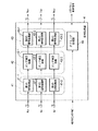
ガンマ補正回路42は、図7に示すように、加算およびオーバフロー処理部421を含む被補正用ビット生成部420、フリップフロップ(FF)422、ガンマ補正用ルックアップテーブルメモリ(単にメモリとも言う)423、および補間演算部424を有する。
【0062】
メモリ423は本発明に係る記憶手段に相当し、補間演算部424は本発明に係る補間手段に相当する。
【0063】
被補正用ビット生成部420は、入力された画像信号の内、所定のビット幅の上位ビットを抽出して被補正用ビットを生成し、所定のビット幅に応じた所定のビットだけその被補正用ビットより大きい被補正用ビットを生成し出力する。
例えば、被補正用ビット生成部420は、加算およびオーバフロー処理部421を含む。
【0064】
加算およびオーバフロー処理部421は、入力画像信号に基づいて、所定のビット幅の上位ビットを抽出した被補正用ビット(A点)に、所定のビット幅に応じた所定のビットだけその被補正用ビット(A点)より大きい補正用ビット(B点)を生成し出力する。
この入力信号の近傍の2点は、ルックアップテーブルの量子化ビットに応じて生成される。
【0065】
加算およびオーバフロー処理部421は、例えば詳細には、後述するメモリ423の所定の量子化ビットで、入力信号の近傍の2点をA点、B点とすると、2点間を直線補間関数で補間するために、12ビット幅の入力信号の上位10ビットの被補正用ビット(A点)の10ビット目に1を加算した被補正用ビット(B点)を生成し、メモリ423に出力する。
具体的には、加算およびオーバフロー処理部421は、入力信号の上位10ビットの信号の10ビット目に1を加算した信号を、メモリ423の各アドレスポートに入力する。
【0066】
フリップフロップ(FF)422は、入力信号を補間演算部424に入力させるタイミングを調整する。
FF422は、入力信号から被補正用ビットを除いた残りの被補間用ビット、より詳細には入力信号の下位2ビットの被補間用ビットを保持し、所定のタイミングで、例えば、メモリ423から補正値データが出力されるタイミングと一致するように補間演算部432に出力する。
【0067】
ガンマ補正用ルックアップテーブルメモリ(メモリ)423は、所定の階調の入力信号の所定のビット幅の上位ビットの被補間用ビットと、ガンマ補正値データとを対応付けたガンマ補正用ルックアップテーブル(LUT)を記憶する。
例えば、メモリ423は、入力信号として上位10ビットの被補正用ビットが入力される場合には、2^10=1024wordのメモリ容量を持つ2つのリードポートを有するデュアルポートメモリで構成され、ガンマ補正値データを格納する。
【0068】
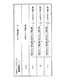
図8は、図7に示したガンマ補正回路のメモリのルックアップテーブル(LUT)を説明するための図である。図8(a)は、入力信号の所定の上位ビットの被補正用ビットであり、メモリ423のアドレスに対応する。図8(b)は、図8(a)で示した入力信号の被補正用ビットに対応するガンマ補正値データである。
【0069】
ガンマ補正値データは、例えば、図4で示したような入力信号レベルと出力信号レベルと対応付けるガンマ補正値データである。
例えば、このガンマ補正値データは、入力信号に応じて表示させた表示画像を、例えばカメラ等の撮像装置で撮像した信号と、入力信号とを比較して比較結果に基づいて生成される。
【0070】
メモリ423は、例えば図8に示すように、入力信号の所定の上位ビットの被補正用ビットに対応するアドレスに、入力信号の所定の上位ビットの被補正用ビットに対応する補正値データを格納する。
【0071】
例えば、メモリ423は、デュアルポートメモリ423であり、A点およびB点に対応する被補正用ビットそれぞれが入力されると、テーブル変換して、その被補正用ビットに対応する補正値データを補間演算部424に出力する。
【0072】
メモリ423では、例えば、ルックアップテーブルを書き込む場合には、書込み指示を含むメモリ制御信号が入力されると、補正値データが所定のアドレスに格納される。また確認等のためにルックアップテーブルを読み出す場合には、読出し指示を含むメモリ制御信号が入力されると、所定のアドレスの補正値データが出力される。
【0073】
補間演算部424は、メモリ423から出力された、A点およびB点の補正値データ、およびFF422から出力された、入力信号から上位ビットを除いた残りの下位ビットの被補間用ビットに基いて、直線補間処理を行う。
【0074】
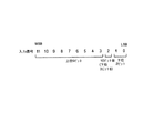
図9は、図7に示した補正回路の補間演算部の動作を説明するための図である。図10は、図7に示した補正回路の補間演算部の入力信号の下位ビットと、ガンマ補正値データとの対応付けを説明するための図である。
【0075】
具体的には、例えば、補間演算部424は、被補間ビットの量子化ビット数を2とすると、A点とB点の補間値データの間を4分割し、各量子化ポイント(1/4、1/2、3/4の点)の補間値データを生成する。
【0076】
また、例えば、被補間用ビットの量子化ビット数が3の場合には、A点とB点の補間値データの間を8分割し、被補間用ビットの量子化ビット数がnの場合には、A点とB点の補間値データの間を2のn乗個に分割し、補間値データを生成する。
この被補間用ビットの量子化ビットを任意の値に設定することで、要求されるメモリ容量や補正精度に対応することができる。
【0077】
補間演算部424は、入力された下位2ビットの被補間用ビットに基いて、生成された補間値データおよび補正値データを選択する。
具体的には、補間演算部424は、例えば図10に示すように、入力信号の下位2ビットの被補間用ビットが、00の場合には、A点のガンマ補正値を出力する。
【0078】
補間演算部424は、入力信号の下位2ビットの被補間用ビットが01の場合には、{(B点のガンマ補正値−A点のガンマ補正値)/2}×(1/4)+A点のガンマ補正値を出力する。
【0079】
補間演算部424は、入力信号の下位2ビットの被補間用ビットが10の場合には、{(B点のガンマ補正値−A点のガンマ補正値)/2}×(1/2)+A点のガンマ補正値を出力する。
【0080】
補間演算部424は、入力信号の下位2ビットの被補間用ビットが11の場合には、{(B点のガンマ補正値−A点のガンマ補正値)/2}×(3/4)+A点のガンマ補正値を出力する。
【0081】
このとき、LCDパネル6のガンマ特性は入力信号に対し、出力信号は必ず増加する非線形関数で示されるため、信号レベルの小さいA点の値と先ほど求めた補間値データを加算し、求めたい入力信号の補正値データを求めることができる。
【0082】
また、補間演算部424の補間処理は、A点およびB点の補正値データに基づいて、下位ビットの被補間用ビットに対応する補間値データを生成して、入力信号の下位ビットの被補間用ビットに応じた補正値データを選択したが、このような形態に限られるものではない。
例えば、A点およびB点の間の補間値データを計算することなく、補間演算部424は、A点およびB点の補正値データと、入力信号の下位ビットの被補間用ビットに基いて、その補間用ビットに対応する補正値データのみを生成してもよい。
【0083】
図11は、図7に示した補正回路の動作を説明するための図である。上述した構成の補正回路42の動作を、図11を参照しながら説明する。
【0084】
あらかじめ、メモリ423に、ガンマ補正値データと2^10=1024wordのメモリ容量の2つのリードポートを有するデュアルポートメモリを使用し、ガンマ補正値データを格納する。
【0085】
ステップST1において、加算およびオーバフロー421では、入力信号に基づいて、入力信号の上位10ビットの被補正用ビットが入力されると、10ビット目に1だけ加算した被補正用ビットが生成され、メモリ423に出力される。また、入力信号の上位10ビットの被補正用ビットは、メモリ423に入力される。
【0086】
ステップST2において、メモリ423では、入力信号の上位10ビットの被補正用ビット(A点)と、加算およびオーバフロー処理部421から出力された入力信号の上位10ビットの10ビット目に1が加算された被補正用ビット(B点)とが、所定のアドレスポートに入力され、被補正用ビットそれぞれに対応するアドレスに格納された補正値データが、補間演算部424に出力される。具体的には、被補正用ビットA点およびB点それぞれに対応する補正値データが、補間演算部424に出力される。
【0087】
ステップST3において、FF422では、入力信号の下位2ビットの被補間用ビットが保持され、所定のタイミングで、補間演算部424に出力される。
補間演算部424では、メモリ423から出力されたA点およびB点の補正値データ、およびFF422から出力された入力信号の下位2ビットの被補間用ビットに基づいて、補間処理が行われる。
【0088】
具体的には、例えば補間演算部424では、被補間用ビットの量子化ビット数は2なので、図9に示すようにA点とB点の間を4分割し、各量子化ポイント(1/4、1/2、3/4の点)の補間値データを求め、下位2ビットの被補間用ビットに基づいて、生成した補間値データおよびA点の補正値データから入力信号に対応する補間値データを選択する。このとき、LCDのガンマ特性は入力信号に対し、出力信号は必ず増加する非線形関数で示されるため、信号レベルの小さいA点の値と先ほど求めた補間値データを加算し、求めたい入力信号レベルのガンマ補正値データを求めることができる。
補間演算部424では補間処理された画像信号を次段の所定の構成要素に出力する。
【0089】
上述したように、例えば、従来のガンマ補正用ルックアップメモリは、12ビット幅の階調をもつ入力信号の場合、2^12=4096wordのメモリ容量を持つメモリを使用し、このメモリにガンマ補正値データを格納することでLUTとしてテーブル変換を行う。これに比べて本実施の形態では、より少ない記憶容量、1024wordのメモリ容量を持つメモリでよい。
【0090】
上述したように、入力画像信号に基づいて、所定のビット幅の上位ビットを抽出した被補正用ビット(A点)に、所定のビット幅に応じた所定のビットだけその被補正用ビット(A点)より大きい被補正用ビット(B点)を生成し出力する加算およびオーバフロー処理部421と、ルックアップテーブル(LUT)を記憶するメモリ423と、タイミング調整用のFF422と、FF422から出力された入力信号の下位ビットの被補正用ビットと、メモリ423から出力された2つの補正値データとに基づいて、補間処理を行う補間演算部424とを設けたので、従来よりも小さいルックアップテーブルを用いて入力画像信号に対応する補正値データを生成することができる。
また、ルックアップテーブル(LUT)を記憶するメモリ423の記憶容量を小さくすることができる。
【0091】
また、入力信号に対してLUTによるテーブル変換を行うために必要なメモリの規模は小さくなるから、メモリ容量の抑制と消費電力増大の抑制が可能となる。
【0092】
また、従来のLUTによる補正回路と比較して、LUTに使用するメモリ規模が小さいため、LUTに格納するためのガンマ補正値データの転送時間を短縮することができ、転送時間削減により、本システムが占有する時間が短縮でき、空いた時間は消費電力の抑制等が可能となる。
【0093】
また、従来、ソフトウェアにより求めていたガンマ補正値データのソフトウェアによる演算処理が不要になり、ソフトウェアは特定のレベルのガンマ補正値データのみ用意すればよい。このため、ソフトウェアの処理時間の短縮やソースコード量の削減をする事が可能となる。
【0094】
第2の実施の形態
図12は、本発明に係る補正回路の第2の実施の形態の機能ブロック図である。
本実施の形態に係る補正回路42aは、図11に示すように、アドレスセレクタ4211、セレクタ4212、FF422a、第1のガンマ補正用ルックアップテーブルメモリ(第1のメモリ)4231および第2のガンマ補正用ルックアップテーブルメモリ(第2のメモリ)4232を含むメモリ423a、データセレクタ4233、ならびに補間演算部424aとを有する。
【0095】
補正回路42aと、第1の実施の形態に係る補正回路42との大きな相違点は、ルックアップテーブルを記憶するメモリを2つ設けている点である。
【0096】
アドレスセレクタ4211は、入力画像信号に基づいて、入力信号の近傍2点をA点、B点の被補正用ビットを生成し、メモリ423aに出力する。
アドレスセレクタ4211は、入力画像信号に基づいて、入力画像信号の内の第1の被補正用ビット、および所定のビット幅に応じた所定のビットだけ第1の被補正用ビットより大きい第2の被補正用ビットを生成し、第1および第2の被補正用ビットそれぞれが偶数または奇数に応じて、後述するメモリ423aに出力する。
【0097】
アドレスセレクタ4211は、例えば、12ビット幅の画像信号が入力された場合には、上位9ビットの被補正用ビット(A点)と、必要に応じてその上位9ビットの被補正用ビットに1を加算した被補正用ビット(B点)を求める。
【0098】
図13は、図11に示した補正回路に入力される信号を説明するための図である。
アドレスセレクタ4221は、例えば、入力信号が12ビットの場合には、図13に示すように、上位9ビットをメモリ423aのアドレスとして用いる。
アドレスセレクタ4221は、例えば入力信号の上位9ビットに基づいて、入力信号の近傍のA点およびB点に対応する補正値を生成するための被補正用ビットを生成する。
【0099】
図14は、図12に示した補正回路のアドレスセレクタの動作を説明するための図である。
アドレスセレクタ4221は、図14に示すように、入力信号が、LSBから3ビット目のデータが0の場合には、後述する第1のメモリ4231(偶数メモリ)に、A点として入力信号の上位9ビットの被補正用ビットをアドレスとして入力する。
また、アドレスセレクタ4221は、第2のメモリ4232(奇数メモリ)に、B点として入力信号の上位9ビットの被補正用ビットをアドレスとして入力する。
【0100】
アドレスセレクタ4221は、入力信号がLSBから3ビット目のデータが1の場合には、第2のメモリ(奇数メモリ)4232に、A点として入力信号の上位9ビットの被補正用ビットをアドレスとして入力する。
また、アドレスセレクタ4221は、第1のメモリ(偶数メモリ)4231に、B点として入力信号の上位9ビットの被補正用ビットに、MSBから9ビット目に1加算した被補正用ビットをアドレスとして入力する。
【0101】
アドレスセレクタ4211は、被補正用ビットのMSBから10ビット目の値が偶数か奇数かに応じて、後述するように、メモリ423aの第1のメモリ4231および第2のメモリ4232のどちらかのメモリにアクセスして補正値データを生成させる。
入力信号の下位2ビットの被補間用ビットは、補間演算部424aにより、補間演算用のパラメータとして用いられる。
【0102】
セレクタ4212は、例えば、入力信号から下位2ビットを抽出して被補間用ビットとしてFF422aに出力する。
セレクタ4212は、例えば、アドレスセレクタ4211から、入力信号から被補正用ビットを除いた残りの被補間用ビットに基づいて下位2ビットを抽出して被補間用ビットとしてFF422aに出力する。
セレクタ4212は、この形態に限られるものではない。例えば、入力信号の下位2ビットを抽出して被補間用ビットとしてFF422aに出力することができればよい。
【0103】
FF422aは、セレクタ4212から出力された入力信号の下位ビットの被補間用ビットを保持し、所定のタイミングで補間演算部424aに出力する。
FF422aは、例えば、補間演算部424aが、データセレクタ4223から出力されたA点およびB点の補正値データと、このFF422aから出力された入力信号の下位ビットの被補間用ビットに基づいて補間処理を行う際に、その処理に適切なタイミングで、例えばデータセレクタ4233から出力される補正値データと同時になるようなタイミングで、入力信号の下位ビットの被補間用ビットを補間演算部424aに出力する。
【0104】
メモリ423aは、複数のメモリ、例えば第1のメモリ4231および第2のメモリ4232とを有する。
例えば、第1のメモリおよび第2のメモリそれぞれは、2^9=512wordのメモリ容量を持つ1つのリードポートを有するシングルポートメモリであり、ガンマ補正値データを含むルックアップテーブルを格納する。
【0105】
図15は、図12に示した補正回路の第1のメモリおよび第2のメモリに記憶されているルックアップテーブルを模式的に示す図である。
図15(a)は、入力信号の上位9ビットの被補正用ビットおよび第1のメモリのアドレスを示し、図15(b)は第1のメモリに記憶されている図15(a)の入力信号に対応するガンマ補正値データの一具体例を示す図である。
図15(c)は、入力信号の上位9ビットの被補正用ビットおよび第2のメモリのアドレスを示し、図15(d)は第2のメモリに記憶されている図15(c)の入力信号に対応するガンマ補正値データの一具体例を示す図である。
【0106】
第1のメモリ4231には、例えば図15(a),(b)に示すように、入力信号のLSBから3ビット目のデータに応じて、入力信号の3ビット目のデータが偶数に対応するガンマ補正値データを格納する。第1のメモリ4231に記憶されている第1のルックアップテーブルは、例えば図15(a),(b)に示すように格納されている。
【0107】
第2のメモリ4232には、例えば図15(c),(d)に示すように、入力信号のLSBから3ビット目のデータに応じて、入力信号の3ビット目のデータが奇数に対応するガンマ補正値データを格納する。第2のメモリ4232に記憶されている第2のルックアップテーブルは、例えば図15(c),(d)に示すように格納されている。
【0108】
データセレクタ4233は、第1のメモリ4231から出力された補正値データと、第2のメモリ4232から出力された補正値データに基づいて、例えば図9に示すように、小さいほうのデータをA点の補正値データ、大きいほうのデータをB点の補正値データとして、補間演算部424aに出力する。
【0109】
補間演算部424aは、データセレクタ4233から出力された、入力信号の近傍2点(A点、B点)のガンマ補正値データと、FF422aから出力された入力信号の下位ビットの被補間用ビットに基づいて、直線補間処理を行い、入力信号のガンマ補正値データを生成し出力する。
補間演算部424aの機能は、第1の実施の形態に係る補正回路の補間演算部424と同様であるので詳細な説明を省略する。
【0110】
上述した構成の動作を簡単に説明する。
あらかじめ、第1のメモリ4231および第2のメモリ4232それぞれに、ガンマ補正値データと2^9=512wordのメモリ容量1つのリードポートを有するシングルポートメモリを使用し、上述したガンマ補正値データを含むルックアップテーブルを格納する。
【0111】
アドレスセレクタ4211では、入力信号に基づいて、例えば図14に示すように、入力信号の近傍2点のA点、B点の被補正用ビットが生成され、それぞれ所定のメモリ423aに入力される。
詳細には、アドレスセレクタ4211では、入力信号に基づいて、入力信号の内の第1の被補正用ビット、および所定のビット幅に応じた所定のビットだけ当該第1の被補正用ビットより大きい第2の被補正用ビットを生成し、第1および第2の被補正用ビットそれぞれが偶数または奇数に応じて、第1のメモリ4231および第2のメモリ4232に出力する。
【0112】
メモリ423aの第1のメモリ4231、および第2のメモリ4232それぞれでは、入力された第1のおよび第2の被補正用ビットに対応する補正値データが、データセレクタ4233に出力される。
データセレクタ4233では、第1のメモリ4231から出力された補正値データと、第2のメモリ4232から出力された補正値データに基づいて、小さいほうのデータをA点の補正値データ、大きいほうのデータをB点の補正データとして、補間演算部424aに出力される。
【0113】
補間演算部424aでは、データセレクタ4233から出力された、入力信号の近傍2点(A点、B点)のガンマ補正値データと、セレクタ4212およびFF422aから出力された入力信号の下位ビットの被補間用ビットに基づいて、直線補間処理が行われ、入力信号のガンマ補正値データを生成し出力する。
【0114】
上述したように、本実施の形態では、入力信号に基づいて、所定の上位ビットを抽出し、入力信号の近傍2点をA点、B点の被補正用ビットを生成し、所定の423aに出力するアドレスセレクタ4211と、入力信号の所定の下位ビットの被補間用ビットを出力するセレクタ4212と、タイミング調整用のFF422aと、入力信号の3ビット目のデータが偶数に対応するガンマ補正値データを格納する第1のメモリ4231と、入力信号の3ビット目のデータが奇数に対応するガンマ補正値データを格納する第2のメモリ4232と、メモリ423aから出力された補正値データに基づいて、小さいほうのデータをA点の補正値データとし大きいほうのデータをB点の補正値データとして補間演算部424aに出力するデータセレクタ4233と、データセレクタ4233から出力された、入力信号の近傍2点(A点、B点)のガンマ補正値データと、FF422aから出力された入力信号の下位ビットの被補間用データに基づいて、直線補間処理を行い、入力信号のガンマ補正値データを生成し出力する補間演算部424aとを設けたので、小さいルックアップテーブルを用いて入力信号に対応する補正値データを生成することができる。
【0115】
また、ルックアップテーブル(LUT)を記憶するメモリ423aの記憶容量を小さくすることができる。
また、2つのメモリを設けたことにより、例えばA点およびB点の補正値データを同時に高速に生成することができるので、補間演算部424aにより早いタイミングで補間演算を行わせることができ、全体としてより高速に補正値データを生成することができる。
【0116】
第3の実施の形態
ルックアップテーブル(LUT)に使用するガンマ補正値データの作成方法として、画像処理装置で表示された画像を、カメラ等で取り込み、画像表示装置の出力信号レベルとデジタル回路の入力信号レベルからガンマ補正値データを算出する。
【0117】
このとき算出されるガンマ補正値データは、量子化ビット数nすべての入力信号のレベルについて作成するのではなく、量子化ビット数(n−m)で作成する。ここで、mとnの関係は1<m<nである。
【0118】
図16は、本発明に係る画像処理装置の第3の実施の形態の機能ブロック図である。
第3の実施の形態に係る画像処理装置の補正回路42bは、例えば図16に示すように、加算およびオーバフロー処理部421b、フリップフロップ(FF)422b、メモリ423b、および補間演算部424bを有する。
【0119】
補正回路42bは、第1の実施の形態に係る補正回路42とほぼ同じ構成である。相違点は、メモリ423bは、上述した量子化ビット数(n−m)で作成されたガンマ補正値データのみをルックアップテーブルとして格納する。
補間演算部424bは、量子化ビット数nの入力信号に対するガンマ補正値データを、メモリ423から出力されるデータ、および入力信号に基づいて補正値の補間処理を行い、入力信号に対応する補正値データを出力する。
【0120】
上述したように、上述の構成の補正回路42bでは、量子化ビット数(n−m)の入力信号のレベルに対応する、ガンマ補正値データに基づいて、補正処理を行うので、所望の補正精度やメモリ容量等を考慮して、所定の量子化ビット(n−m)の補正データを記憶することができる。
これにより、従来ソフトウェアにて補間演算して求めたガンマ補正値データも不要となる。
【0121】
なお、本発明は本実施の形態に限られるものではなく、任意好適な種々の改変が可能である。
例えば、入力ビット数を12ビット、LUTの入力ビット数を、実施の実施の形態では、10ビット、第2の実施の形態では9ビット、補間する領域のビット数を2ビット、システムの出力ビット数を12ビットとして説明したが、本発明は、この形態に限られるものではない。各ビット数の値を限定するものではない。
【0122】
また、表示デバイスとして、ノーマリホワイト透過型液晶のV−T特性を例として説明したが、ノーマリブラック液晶、反射型液晶におけるデジタルガンマ補正においても有効である。さらに、CRTなど、液晶以外の同様な非線型の応答をする表示デバイスにおけるデジタルガンマ補正においても同様に有効である。
【0123】
また、画像信号を出力デバイスの特性に合わせるために必要量より少ないルックアップテーブルと必要量に不足するデータを補間するための補間関数を使用したガンマ補正を行うことで、テーブル変換に必要なメモリの規模を小さくする事が可能となる。
【0124】
【発明の効果】
本発明によれば、回路規模を増大することなく、補正を行うことができる画像処理装置、および画像処理方法を提供することができる。
【図面の簡単な説明】
【図1】本発明に係る画像処理装置の一実施の形態の機能ブロック図である。
【図2】LCD(液晶)パネルの印加電圧に対する透過率の特性(V−T特性)を示す図である。
【図3】入力信号レベルに対する理想透過率特性を示す図である。
【図4】ガンマ補正カーブを示す図である。
【図5】図1に示した画像処理装置の信号処理部の構成を示す機能ブロック図である。
【図6】図5に示した信号処理部の機能ブロックの一具体例を示す図である。
【図7】図5に示したガンマ補正回路の第1の実施の形態の機能ブロック図である。
【図8】図7に示したガンマ補正回路のメモリのルックアップテーブル(LUT)を説明するための図である。
【図9】図7に示した補正回路の補間演算部の動作を説明するための図である。
【図10】図7に示した補正回路の補間演算部の入力信号の下位ビットと、ガンマ補正値データとの対応付けを説明するための図である。
【図11】図7に示したガンマ補正回路の動作を説明するための図である。
【図12】本発明に係る画像処理装置の補正回路の第2の実施の形態の機能ブロック図である。
【図13】図11に示した補正回路に入力される信号を説明するための図である。
【図14】図12に示した補正回路のアドレスセレクタの動作を説明するための図である。
【図15】図12に示した補正回路の第1のメモリおよび第2のメモリに記憶されているルックアップテーブルを模式的に示す図である。
【図16】本発明に係る画像処理装置の補正回路の第3の実施の形態の機能ブロック図である。
【符号の説明】
1…画像処理装置、2…A/DPLL、3…スキャンコンバータ、4…信号処理部、5…S/Hドライバ、6…LCDパネル、7…XTL、41…第1の信号処理部、42…補正回路、43…第2の信号処理部、44…タイミング生成部、411…ユーザゲイン、412…ユーザブライト、413…サブゲイン、414…サブブライト、415…黒枠、416…第1のミュート、417…パターンジェネレータ、418…OSD、420…被補正用信号生成部、421…加算およびオーバフロー処理部、422…FF、423…補間演算部、424…メモリ、424a…補間演算部、424b…補間演算部、431…ガンマゲイン、432…ガンマブライト、432…補間演算部、433…色むら補正、434…ドットライン反転、435…第2のミュート、436…リミッタ、437…ゴーストキャンセル、438…縦筋キャンセル、4211…アドレスセレクタ、4212…セレクタ、4221…アドレスセレクタ、4223…データセレクタ、4231…第1のメモリ、4232…第2のメモリ、4233…データセレクタ。[0001]
TECHNICAL FIELD OF THE INVENTION
The present invention relates to, for example, an image processing apparatus that performs an image signal correction process, and an image processing method.
[0002]
[Prior art]
2. Description of the Related Art Conventionally, for example, in an image processing apparatus, as a circuit for performing correction of an image signal, for example, gamma correction, a correction circuit that performs correction based on a look-up table (hereinafter referred to as an LUT) or a break point correction using a digital circuit is known. (See, for example, Patent Document 1).
[0003]
In recent years, the LUT-type digital correction circuit is becoming mainstream in recent years because of its high correction accuracy.
[0004]
[Patent Document 1]
JP 2001-320607 A
[0005]
[Problems to be solved by the invention]
In the above-described conventional LUT type digital correction circuit, a memory having 2 ^ n memory addresses is used as the LUT, where n is the number of quantization bits of the input signal. Gamma correction value data corresponding to the input signal level is stored in the LUT, and gamma correction is performed in consideration of the transmittance characteristic (VT characteristic) with respect to the applied voltage of the image display device.
[0006]
However, as the resolution for quantizing the input signal level increases, the size of the memory used for this LUT increases.
For example, when the number of quantization bits at the input signal level is 10 bits, the capacity required for the memory used for the LUT is 1024 words, and when the number of quantization bits at the input level is 12 bits, 4096 words is required.
[0007]
As described above, when the 1-bit resolution increases, the memory capacity increases twice. Accordingly, there has been a problem that the circuit scale increases, the power consumption increases, and the update time of the gamma correction value data stored in the memory increases.
[0008]
The present invention has been made in view of such circumstances, and an object of the present invention is to provide an image processing apparatus and an image processing method capable of performing correction without increasing the circuit scale.
[0009]
[Means for Solving the Problems]
In order to achieve the above object, an image processing apparatus according to a first aspect of the present invention is an image processing apparatus for performing a correction process on an image signal composed of a plurality of bits, and performs table conversion of bits to be corrected in the image signal. Storage means for storing correction value data, and first correction value data table-converted by the storage means based on the first bit to be corrected in the input image signal; and the first bit to be corrected. The second correction value data table-converted by the storage unit based on the second bit to be corrected which is larger than the second bit to be corrected, and the remaining bits to be interpolated by removing the bit to be corrected from the input image signal. Interpolating means for performing interpolation processing to generate third correction value data for the input image signal.
[0010]
According to the image processing apparatus of the first invention, a correction process of an image signal including a plurality of bits is performed.
The storage unit stores correction value data for converting a bit to be corrected in the image signal into a table.
In the interpolation means, the first correction value data table-converted by the storage means based on the first bit to be corrected in the input image signal, the second correction value larger than the first bit to be corrected. The second correction value data table-converted by the storage means on the basis of the input bits, and the remaining interpolated bits obtained by removing the bits to be corrected from the input image signal, perform interpolation processing on the input image signal. 3 is generated.
[0011]
Further, in order to achieve the above object, the image processing method according to the second aspect of the present invention converts a bit to be corrected in an image signal composed of a plurality of bits into a table based on preset correction value data, and An image processing method for an image processing apparatus that performs signal correction processing, wherein the table conversion is performed based on a first bit to be corrected in an input image signal to generate first correction value data, and the first correction value data is generated. Converts the table based on a second bit to be corrected larger than one bit to be corrected to generate second correction value data, and generates the first and second correction value data and the input image signal. Then, based on the remaining bits to be interpolated except for the bits to be corrected, interpolation processing is performed to generate third correction value data for the input image signal.
[0012]
BEST MODE FOR CARRYING OUT THE INVENTION
An image processing apparatus according to the present invention generates a correction value based on a look-up table for correcting an image signal, and further performs an interpolation process on the correction value to generate a correction value of the image signal.
Hereinafter, an embodiment of an image processing apparatus according to the present invention will be described with reference to the drawings.
First embodiment
An image processing apparatus according to a first embodiment of the present invention is an image processing apparatus using a display device such as a liquid crystal which makes a nonlinear optical response to an input signal level of an image signal. The correction value generated based on the up table and the input image signal and the lookup table is interpolated by a linear correction function.
More specifically, in order to match the image signal with the characteristics of the output device, gamma correction is performed using a lookup table smaller than the required amount and an interpolation function for interpolating the data lacking the required amount.
[0013]
Hereinafter, a front / rear projector system using an LCD panel employing the correction circuit of the image processing apparatus according to the present embodiment will be described.
FIG. 1 is a functional block diagram of an embodiment of an image processing apparatus according to the present invention. As shown in FIG. 1, the
[0014]
In the
[0015]
The A /
[0016]
The A /
Further, the A /
[0017]
The
[0018]
The
The
[0019]
The
[0020]
The
[0021]
The
The
[0022]
The sample / hold (S / H)
[0023]
The S /
[0024]
The
The
[0025]
For example, the LCD panel 6-1 displays an image corresponding to a 6-bit R signal output from the S / H drivers 5-1 and 5-2 and a predetermined signal output from the
[0026]
For example, the LCD panel 6-2 displays an image corresponding to a 6-bit G signal output from the S / H drivers 5-3 and 4 and a predetermined signal output from the
For example, the LCD panel 6-3 displays an image corresponding to a 6-bit B signal output from the S / H drivers 5-5 and 6 and a predetermined signal output from the
[0027]
The operation of the
The analog video signal is A / D-converted by an A / DPLL (converter) 2, subjected to scaling and dithering processing by a
[0028]
The digital data is input to the
The output image signal is sampled / held by a sample /
[0029]
FIG. 2 is a diagram showing characteristics of transmittance (VT characteristics) with respect to an applied voltage of an LCD (liquid crystal) panel.
In the LCD (liquid crystal)
[0030]
FIG. 3 is a diagram showing ideal transmittance characteristics with respect to an input signal level. FIG. 4 is a diagram showing a gamma correction curve.
For the display luminance in the
Due to the requirement of the conditions of these two characteristics, the output signal level (liquid crystal applied voltage) with respect to the input signal level needs to be nonlinearly corrected as shown in FIG. 4, and this correction is called gamma correction.
[0031]
For example, an image displayed by the
[0032]
When performing the correction based on the input signal, the image processing apparatus including the correction circuit according to the present embodiment outputs the gamma correction value data corresponding to the input signal with reference to the look-up table. When the level of the input signal is between predetermined quantization bit intervals in the look-up table, interpolation processing is performed based on the input signal and the look-up table to output gamma correction value data.
[0033]
FIG. 5 is a functional block diagram illustrating a configuration of a signal processing unit of the image processing apparatus illustrated in FIG.
The
[0034]
The first
For example, the first
[0035]
The
For example, the
[0036]
The second
For example, the second
[0037]
The
[0038]
In the
[0039]
The G signal Gin is processed by the first signal processing unit 41-2, processed by the gamma correction circuit 42-2, processed by the second signal processing unit 43-2, and a G signal Gout # is output as a processing result. You.
[0040]
The B signal Bin is processed by the first signal processing unit 41-3, processed by the gamma correction circuit 42-3, processed by the second signal processing unit 43-3, and a B signal Bout # is output as a processing result. You.
[0041]
FIG. 6 is a diagram illustrating a specific example of a functional block of the signal processing unit illustrated in FIG. For example, in more detail, as shown in FIG. 6, the
[0042]
Each functional block will be briefly described. Note that parameters such as coefficients used in each functional block are set from, for example, a host device (not shown) via a host I / F (not shown).
[0043]
The
[0044]
The user bright 412 performs addition and subtraction processing as brightness adjustment for user control.
The user bright 412 calculates a 12-bit input signal output from the
[0045]
The
The calculation of the
[0046]
The sub-bright 414 performs addition and subtraction processing as bright adjustment for white balance.
The operation of the sub-bright 414 is performed, for example, by performing addition and subtraction processing on the basis of a 12-bit input signal output from the sub-gain 413 and a predetermined coefficient (MSB is a sign bit) to convert the 12-bit data into a black frame (block). ) 415.
[0047]
A black frame (block) 415 performs processing for fixing the blanking period of the image signal to an arbitrary level regardless of the result of the preceding signal processing.
[0048]
A black frame (block) 415 indicates that when the number of pixels determined from the effective period of the image signal to be displayed is less than the number of pixels of the
Here, an arbitrary range of the image signal is replaced with 12-bit data by switching the image signal and the coefficient by using a pulse output from a pulse decoder (not shown), and the 12-bit data is converted to the first mute 416. Output.
[0049]
The first mute 416 replaces a 12-bit input signal with data of an arbitrary level to perform a mute process, and outputs the processed 12-bit data to a
[0050]
The
[0051]
The
[0052]
The
[0053]
The
[0054]
The gamma bright 432 performs addition and subtraction processing as bright adjustment for correcting variations in the VT characteristics of the
[0055]
The
[0056]
The
[0057]
The second mute 435 replaces the video signal output from the
[0058]
The
[0059]
The ghost cancel 437 corrects, for example, a ghost generated inside the
The vertical stripe cancel 438 performs a correction process for reducing vertical stripes generated in the
[0060]
For example, each functional block of the
[0061]
FIG. 7 is a functional block diagram of the first embodiment according to the gamma correction circuit shown in FIG.
As shown in FIG. 7, the
[0062]
The
[0063]
The to-be-corrected
For example, the bit generation unit for
[0064]
The addition and
Two points near the input signal are generated according to the quantization bits of the look-up table.
[0065]
The addition and
Specifically, the addition and
[0066]
The flip-flop (FF) 422 adjusts the timing at which an input signal is input to the
The
[0067]
The gamma correction look-up table memory (memory) 423 is a gamma correction look-up table that associates higher-order bits to be interpolated with a predetermined bit width of an input signal of a predetermined gradation with gamma correction value data. (LUT) is stored.
For example, when the upper 10 bits to be corrected are input as an input signal, the
[0068]
FIG. 8 is a diagram for explaining a look-up table (LUT) of the memory of the gamma correction circuit shown in FIG. FIG. 8A shows bits to be corrected of predetermined upper bits of the input signal, which correspond to addresses in the
[0069]
The gamma correction value data is, for example, gamma correction value data that associates an input signal level with an output signal level as shown in FIG.
For example, the gamma correction value data is generated based on a result of comparing a display image displayed according to an input signal with a signal captured by an imaging device such as a camera and the input signal.
[0070]
For example, as shown in FIG. 8, the
[0071]
For example, the
[0072]
In the
[0073]
The
[0074]
FIG. 9 is a diagram for explaining the operation of the interpolation calculation unit of the correction circuit shown in FIG. FIG. 10 is a diagram for explaining the association between the lower bits of the input signal of the interpolation operation unit of the correction circuit shown in FIG. 7 and gamma correction value data.
[0075]
Specifically, for example, assuming that the number of quantized bits of the bit to be interpolated is 2, the
[0076]
Further, for example, when the number of quantized bits of the bit to be interpolated is 3, the interpolated value data at the points A and B is divided into eight, and when the number of quantized bits of the bit to be interpolated is n, Divides the interpolated value data at points A and B into 2 n powers to generate interpolated value data.
By setting the quantization bit of the bit to be interpolated to an arbitrary value, it is possible to cope with a required memory capacity and correction accuracy.
[0077]
The
Specifically, for example, as shown in FIG. 10, when the lower 2 bits of the input signal to be interpolated are 00, the
[0078]
When the lower 2 bits of the input signal to be interpolated are 01, the
[0079]
When the lower 2 bits of the input signal to be interpolated are 10, the
[0080]
When the lower 2 bits of the input signal to be interpolated are 11, the
[0081]
At this time, since the gamma characteristic of the
[0082]
Further, the interpolation processing of the
For example, without calculating the interpolation value data between the points A and B, the
[0083]
FIG. 11 is a diagram for explaining the operation of the correction circuit shown in FIG. The operation of the
[0084]
The gamma correction value data is stored in the
[0085]
In step ST1, in addition and
[0086]
In step ST2, the
[0087]
In step ST3, the
The
[0088]
Specifically, for example, in the
The
[0089]
As described above, for example, a conventional gamma correction look-up memory uses a memory having a memory capacity of 2 ^ 12 = 4096 words in the case of an input signal having a 12-bit width gradation. By storing the value data, table conversion is performed as an LUT. In contrast, in the present embodiment, a memory having a smaller storage capacity and a memory capacity of 1024 words may be used.
[0090]
As described above, based on the input image signal, the bits to be corrected (points A) obtained by extracting the upper bits of a predetermined bit width are added to the bits to be corrected (A) by a predetermined bit corresponding to the predetermined bit width. ), An addition and
Further, the storage capacity of the
[0091]
Further, since the size of the memory required for performing the table conversion by the LUT on the input signal is reduced, it is possible to suppress the memory capacity and the power consumption.
[0092]
In addition, since the memory scale used for the LUT is smaller than that of a correction circuit using a conventional LUT, the transfer time of gamma correction value data to be stored in the LUT can be reduced. Occupied time can be shortened, and during the vacant time, power consumption can be suppressed.
[0093]
In addition, it is not necessary to perform the arithmetic processing of the gamma correction value data conventionally obtained by software by software, and the software only needs to prepare gamma correction value data of a specific level. For this reason, it is possible to reduce the processing time of software and the amount of source code.
[0094]
Second embodiment
FIG. 12 is a functional block diagram of a second embodiment of the correction circuit according to the present invention.
As shown in FIG. 11, the
[0095]
A major difference between the
[0096]
The
Based on the input image signal, the
[0097]
For example, when a 12-bit width image signal is input, the
[0098]
FIG. 13 is a diagram for explaining signals input to the correction circuit shown in FIG.
For example, when the input signal is 12 bits, the address selector 4221 uses the upper 9 bits as the address of the
The address selector 4221 generates bits to be corrected for generating correction values corresponding to points A and B near the input signal based on, for example, the upper 9 bits of the input signal.
[0099]
FIG. 14 is a diagram for explaining the operation of the address selector of the correction circuit shown in FIG.
As shown in FIG. 14, when the input signal is 0 in the third bit from the LSB, the address selector 4221 sets the point A in the first memory 4231 (even memory), which will be described later, 9 bits to be corrected are input as an address.
In addition, the address selector 4221 inputs, to the second memory 4232 (odd number memory), the upper 9 bits to be corrected of the input signal as the point B as an address.
[0100]
When the third bit from the LSB of the input signal is 1, the address selector 4221 sets the point A to the second memory (odd-numbered memory) 4232 as the point A using the upper 9 bits of the input signal as the address to be corrected. input.
In addition, the address selector 4221 uses the first memory (even memory) 4231 as an address with the corrected bit obtained by adding the first 9 bits from the MSB to the 9 higher-order bits of the input signal as a point B. input.
[0101]
The
The lower 2 bits to be interpolated of the input signal are used by the
[0102]
The
The
The
[0103]
The
The
[0104]
The
For example, each of the first memory and the second memory is a single-port memory having one read port having a memory capacity of 2 ^ 9 = 512 words, and stores a look-up table including gamma correction value data.
[0105]
FIG. 15 is a diagram schematically showing a lookup table stored in the first memory and the second memory of the correction circuit shown in FIG.
FIG. 15A shows the upper 9 bits to be corrected of the input signal and the address of the first memory, and FIG. 15B shows the input of FIG. 15A stored in the first memory. FIG. 7 is a diagram illustrating a specific example of gamma correction value data corresponding to a signal.
FIG. 15C shows the upper 9 bits to be corrected of the input signal and the address of the second memory, and FIG. 15D shows the input of FIG. 15C stored in the second memory. FIG. 7 is a diagram illustrating a specific example of gamma correction value data corresponding to a signal.
[0106]
In the
[0107]
In the
[0108]
The
[0109]
The
The function of the
[0110]
The operation of the above configuration will be briefly described.
The
[0111]
In the
Specifically, in the
[0112]
In each of the
In the
[0113]
In the
[0114]
As described above, in the present embodiment, a predetermined higher-order bit is extracted based on an input signal, and two points near the input signal are generated as bits to be corrected at points A and B, and the bits are corrected to a predetermined 423a. An
[0115]
Further, the storage capacity of the
Further, since the two memories are provided, for example, the correction value data of the points A and B can be simultaneously generated at a high speed, so that the
[0116]
Third embodiment
As a method of generating gamma correction value data used for a look-up table (LUT), an image displayed by an image processing device is captured by a camera or the like, and gamma correction is performed based on an output signal level of the image display device and an input signal level of a digital circuit. Calculate the value data.
[0117]
The gamma correction value data calculated at this time is not created for all input signal levels of the quantization bit number n, but is created with the quantization bit number (nm). Here, the relationship between m and n is 1 <m <n.
[0118]
FIG. 16 is a functional block diagram of the third embodiment of the image processing apparatus according to the present invention.
The
[0119]
The
The
[0120]
As described above, the
As a result, the gamma correction value data obtained by performing the interpolation calculation using the conventional software is not required.
[0121]
Note that the present invention is not limited to the present embodiment, and various suitable modifications are possible.
For example, the number of input bits is 12 bits, the number of input bits of the LUT is 10 bits in the embodiment, 9 bits in the second embodiment, the number of bits of the area to be interpolated is 2 bits, and the number of output bits of the system is Although the number is described as being 12 bits, the present invention is not limited to this form. It does not limit the value of each bit number.
[0122]
Also, the VT characteristic of a normally white transmission type liquid crystal has been described as an example of a display device, but it is also effective in digital gamma correction of a normally black liquid crystal and a reflection type liquid crystal. Further, the present invention is similarly effective in digital gamma correction in a display device that responds similarly in a non-linear manner, such as a CRT, other than liquid crystal.
[0123]
Also, by performing gamma correction using a look-up table that is smaller than the required amount to match the image signal to the characteristics of the output device and an interpolation function to interpolate the data that is insufficient, the memory required for table conversion is obtained. Can be reduced in size.
[0124]
【The invention's effect】
According to the present invention, it is possible to provide an image processing apparatus and an image processing method that can perform correction without increasing the circuit scale.
[Brief description of the drawings]
FIG. 1 is a functional block diagram of an embodiment of an image processing apparatus according to the present invention.
FIG. 2 is a diagram illustrating characteristics of transmittance (VT characteristics) with respect to an applied voltage of an LCD (liquid crystal) panel.
FIG. 3 is a diagram illustrating ideal transmittance characteristics with respect to an input signal level;
FIG. 4 is a diagram showing a gamma correction curve.
FIG. 5 is a functional block diagram illustrating a configuration of a signal processing unit of the image processing apparatus illustrated in FIG. 1;
FIG. 6 is a diagram illustrating a specific example of a functional block of a signal processing unit illustrated in FIG. 5;
FIG. 7 is a functional block diagram of a first embodiment of the gamma correction circuit shown in FIG.
8 is a diagram for explaining a look-up table (LUT) of a memory of the gamma correction circuit shown in FIG. 7;
FIG. 9 is a diagram for explaining an operation of an interpolation operation unit of the correction circuit shown in FIG. 7;
FIG. 10 is a diagram for explaining correspondence between lower-order bits of an input signal of an interpolation operation unit of the correction circuit shown in FIG. 7 and gamma correction value data.
11 is a diagram for explaining the operation of the gamma correction circuit shown in FIG.
FIG. 12 is a functional block diagram of a correction circuit of the image processing apparatus according to the second embodiment of the present invention.
FIG. 13 is a diagram for explaining signals input to the correction circuit shown in FIG. 11;
14 is a diagram for explaining an operation of the address selector of the correction circuit shown in FIG.
15 is a diagram schematically illustrating a lookup table stored in a first memory and a second memory of the correction circuit illustrated in FIG. 12;
FIG. 16 is a functional block diagram of a correction circuit of an image processing apparatus according to a third embodiment of the present invention.
[Explanation of symbols]
DESCRIPTION OF
Claims (10)
画像信号の内の被補正用ビットをテーブル変換するための補正値データを記憶する記憶手段と、
入力画像信号の内の第1の被補正用ビットに基づいて前記記憶手段によりテーブル変換された第1の補正値データ、当該第1の被補正用ビットよりも大きい第2の被補正用ビットに基づいて前記記憶手段によりテーブル変換された第2の補正値データ、および前記入力画像信号から前記被補正用ビットを除いた残りの被補間用ビットに基づいて、補間処理を行い前記入力画像信号に対する第3の補正値データを生成する補間手段とを有する
画像処理装置。An image processing device that performs a correction process on an image signal including a plurality of bits,
Storage means for storing correction value data for converting a bit to be corrected in the image signal into a table,
The first correction value data table-converted by the storage unit based on the first bit to be corrected in the input image signal, and the second bit to be corrected that is larger than the first bit to be corrected. Based on the second correction value data table-converted by the storage means based on the input image signal and the remaining bits to be interpolated except the bits to be corrected from the input image signal, an interpolation process is performed on the input image signal. An image processing apparatus having interpolation means for generating third correction value data.
請求項1に記載の画像処理装置。2. The image processing apparatus according to claim 1, wherein the interpolation unit performs a linear interpolation process based on the first and second correction value data and the bit to be interpolated to generate the third correction value data. 3. .
請求項1に記載の画像処理装置。The interpolation means generates interpolation value data between the first and second correction value data based on the first and second correction value data and the number of quantization bits of the bit to be interpolated. 2. The data according to claim 1, wherein data corresponding to the bit to be interpolated is extracted from the interpolation value data and the first correction value data, and the extracted data is used as the third correction value data. Image processing device.
奇数の前記被補正値用ビットをテーブル変換するための補正値データを記憶する奇数用補正値データ記憶手段とを含み、
前記入力画像信号の内の第1の被補正用ビットに基づいて、当該第1の被補正用ビットよりも大きい第2の被補正用ビットを生成し、前記第1および第2の被補正用ビットそれぞれが偶数または奇数に応じて、前記偶数用補正値データ記憶手段または前記奇数用補正値データ記憶手段に出力する被補正用ビット生成手段とを有し、
前記補間手段は、前記記憶手段によりテーブル変換された第1および第2の補正値データ、ならびに前記被補間用ビットに基づいて補間処理を行い前記第3の補正値データを生成する
請求項1に記載の画像処理装置。The storage means, even-number correction value data storage means for storing correction value data for table conversion of the even-number of bits to be corrected,
An odd-number correction value data storage unit that stores correction value data for converting the odd-number of bits to be corrected into a table.
Generating a second to-be-corrected bit larger than the first to-be-corrected bit based on the first to-be-corrected bit of the input image signal; A bit generation unit for outputting to the even-number correction value data storage unit or the odd-number correction value data storage unit according to whether each bit is even or odd,
2. The interpolator according to claim 1, wherein the interpolator performs an interpolation process based on the first and second correction value data table-converted by the storage unit and the bit to be interpolated to generate the third correction value data. 3. The image processing apparatus according to claim 1.
請求項1に記載の画像処理装置。The image processing apparatus according to claim 1, further comprising a display unit configured to perform a display according to the third correction value data.
入力画像信号の内の第1の被補正用ビットに基づいて前記テーブル変換して第1の補正値データを生成し、
当該第1の被補正用ビットよりも大きい第2の被補正用ビットに基づいて前記テーブル変換して第2の補正値データを生成し、
当該第1および第2の補正値データ、ならびに前記入力画像信号から前記被補正用ビットを除いた残りの被補間用ビットに基づいて、補間処理を行い前記入力画像信号に対する第3の補正値データを生成する
画像処理方法。An image processing method of an image processing apparatus that performs a table conversion of bits to be corrected in an image signal composed of a plurality of bits based on correction value data set in advance, and performs a correction process on the image signal.
Converting the table based on a first bit to be corrected in the input image signal to generate first correction value data;
Converting the table based on a second bit to be corrected larger than the first bit to be corrected to generate second correction value data;
Interpolation processing is performed based on the first and second correction value data and the remaining bits to be interpolated from the input image signal excluding the bits to be corrected, and third correction value data for the input image signal An image processing method for generating an image.
請求項6に記載の画像処理方法。When generating the third correction value data, the third correction value data is generated by performing linear interpolation processing based on the first and second correction value data and the bit to be interpolated. The image processing method according to claim 6.
前記補間値データおよび前記第1の補正値データから、前記被補間用ビットに対応するデータを抽出して、当該抽出されたデータを前記第3の補正値データとする
請求項6に記載の画像処理方法。When generating the third correction value data, the first and second correction value data are generated based on the first and second correction value data and the number of quantization bits of the bit to be interpolated. Generate interpolated value data between
The image according to claim 6, wherein data corresponding to the bit to be interpolated is extracted from the interpolation value data and the first correction value data, and the extracted data is used as the third correction value data. Processing method.
前記第1および第2の被補正用ビットそれぞれが偶数または奇数に応じて、前記記憶している前記補正値データによりテーブル変換された第1および第2の補正値データ、ならびに前記被補間用ビットに基づいて補間処理を行い前記第3の補正値データを生成する
請求項6に記載の画像処理方法。The correction value data for converting the even-numbered bits for corrected values into a table and the correction value data for converting the odd-numbered bits for corrected values into a table are stored, and the third correction value data is generated. In this case, based on the first bit to be corrected in the input image signal, a second bit to be corrected that is larger than the first bit to be corrected is generated,
The first and second correction value data table-converted by the stored correction value data according to whether the first and second correction target bits are even or odd, respectively, and the interpolation target bit The image processing method according to claim 6, wherein the third correction value data is generated by performing an interpolation process based on the third correction value data.
請求項6に記載の画像処理方法。The image processing method according to claim 6, wherein display is performed according to the third correction value data.
Priority Applications (1)
| Application Number | Priority Date | Filing Date | Title |
|---|---|---|---|
| JP2002281145A JP2004120366A (en) | 2002-09-26 | 2002-09-26 | Image processing apparatus and image processing method |
Applications Claiming Priority (1)
| Application Number | Priority Date | Filing Date | Title |
|---|---|---|---|
| JP2002281145A JP2004120366A (en) | 2002-09-26 | 2002-09-26 | Image processing apparatus and image processing method |
Publications (1)
| Publication Number | Publication Date |
|---|---|
| JP2004120366A true JP2004120366A (en) | 2004-04-15 |
Family
ID=32275672
Family Applications (1)
| Application Number | Title | Priority Date | Filing Date |
|---|---|---|---|
| JP2002281145A Pending JP2004120366A (en) | 2002-09-26 | 2002-09-26 | Image processing apparatus and image processing method |
Country Status (1)
| Country | Link |
|---|---|
| JP (1) | JP2004120366A (en) |
Cited By (6)
| Publication number | Priority date | Publication date | Assignee | Title |
|---|---|---|---|---|
| JP2007128045A (en) * | 2005-10-07 | 2007-05-24 | Seiko Epson Corp | Image display system, image display apparatus, and image correction processing program |
| JP2009094947A (en) * | 2007-10-11 | 2009-04-30 | Sanyo Electric Co Ltd | Correction arithmetic circuit |
| JP2011059657A (en) * | 2009-09-09 | 2011-03-24 | Samsung Electronics Co Ltd | Display device |
| US8451200B2 (en) | 2006-12-11 | 2013-05-28 | Sony Corporation | Image processing apparatus, image processing method, display apparatus, and projection display apparatus |
| JP2013243611A (en) * | 2012-05-22 | 2013-12-05 | Funai Electric Co Ltd | Image display device, and lut adjustment method |
| CN109036333A (en) * | 2018-09-17 | 2018-12-18 | 广州视源电子科技股份有限公司 | Display parameter correction method and device of display, terminal equipment and storage medium |
-
2002
- 2002-09-26 JP JP2002281145A patent/JP2004120366A/en active Pending
Cited By (7)
| Publication number | Priority date | Publication date | Assignee | Title |
|---|---|---|---|---|
| JP2007128045A (en) * | 2005-10-07 | 2007-05-24 | Seiko Epson Corp | Image display system, image display apparatus, and image correction processing program |
| US8451200B2 (en) | 2006-12-11 | 2013-05-28 | Sony Corporation | Image processing apparatus, image processing method, display apparatus, and projection display apparatus |
| JP2009094947A (en) * | 2007-10-11 | 2009-04-30 | Sanyo Electric Co Ltd | Correction arithmetic circuit |
| US8089490B2 (en) | 2007-10-11 | 2012-01-03 | Sanyo Electric Co., Ltd. | Correction arithmetic circuit |
| JP2011059657A (en) * | 2009-09-09 | 2011-03-24 | Samsung Electronics Co Ltd | Display device |
| JP2013243611A (en) * | 2012-05-22 | 2013-12-05 | Funai Electric Co Ltd | Image display device, and lut adjustment method |
| CN109036333A (en) * | 2018-09-17 | 2018-12-18 | 广州视源电子科技股份有限公司 | Display parameter correction method and device of display, terminal equipment and storage medium |
Similar Documents
| Publication | Publication Date | Title |
|---|---|---|
| US8035660B2 (en) | Liquid crystal display with corrected image data and method of driving the liquid crystal display | |
| TWI423655B (en) | Image processing device, image processing method, display device, and projection display device | |
| US6278496B1 (en) | Digital correction circuit and image data processing apparatus equipped with a digital correction circuit | |
| JP5449404B2 (en) | Display device | |
| JP2001343957A (en) | Liquid crystal display | |
| WO2006030842A1 (en) | Display apparatus driving method, driving apparatus, program thereof, recording medium and display apparatus | |
| CN101162571B (en) | Liquid crystal display and method of driving the same | |
| JP4824206B2 (en) | Display data processing circuit and liquid crystal display device | |
| US7663678B2 (en) | Gamma correction, image processing method and program, gamma correction circuit, image processing apparatus, and display apparatus | |
| CN113808550A (en) | Applicable to devices for brightness enhancement in display modules | |
| JPH1013849A (en) | PDP gamma correction method | |
| JP2004120366A (en) | Image processing apparatus and image processing method | |
| JPH1132237A (en) | Gamma correction device | |
| JP2002108298A (en) | Digital signal processing circuit and processing method thereof, display device, liquid crystal display device, and liquid crystal projector | |
| JP4892222B2 (en) | Image display device and its correction device | |
| US20070153021A1 (en) | Data converting circuit and display apparatus using the same | |
| JP2008015123A (en) | Display device and driving method thereof | |
| JPH05216430A (en) | Data driver | |
| JP2009265260A (en) | Display method and display device | |
| JP2005260405A (en) | Image processing apparatus and image processing method | |
| US20040227712A1 (en) | Image processing method, image processing apparatus, and liquid crystal display using same | |
| JP3867386B2 (en) | Video display device | |
| JP4720088B2 (en) | Gradation correction circuit, image display device, and image processing method | |
| JP4815749B2 (en) | Image processing device | |
| JP5132081B2 (en) | Display device |
Legal Events
| Date | Code | Title | Description |
|---|---|---|---|
| A621 | Written request for application examination |
Free format text: JAPANESE INTERMEDIATE CODE: A621 Effective date: 20050805 |
|
| A977 | Report on retrieval |
Free format text: JAPANESE INTERMEDIATE CODE: A971007 Effective date: 20071129 |
|
| A131 | Notification of reasons for refusal |
Free format text: JAPANESE INTERMEDIATE CODE: A131 Effective date: 20071204 |
|
| A02 | Decision of refusal |
Free format text: JAPANESE INTERMEDIATE CODE: A02 Effective date: 20080401 |