JP2004142003A - Polishing apparatus and polishing method - Google Patents
Polishing apparatus and polishing method Download PDFInfo
- Publication number
- JP2004142003A JP2004142003A JP2002308771A JP2002308771A JP2004142003A JP 2004142003 A JP2004142003 A JP 2004142003A JP 2002308771 A JP2002308771 A JP 2002308771A JP 2002308771 A JP2002308771 A JP 2002308771A JP 2004142003 A JP2004142003 A JP 2004142003A
- Authority
- JP
- Japan
- Prior art keywords
- polishing
- head
- polishing tape
- head chip
- moving
- Prior art date
- Legal status (The legal status is an assumption and is not a legal conclusion. Google has not performed a legal analysis and makes no representation as to the accuracy of the status listed.)
- Withdrawn
Links
Images


Landscapes
- Finish Polishing, Edge Sharpening, And Grinding By Specific Grinding Devices (AREA)
- Adjustment Of The Magnetic Head Position Track Following On Tapes (AREA)
Abstract
【課題】ブレンド加工を施すに際して、加工工程が簡略化され、生産効率の改善を図る薄膜磁気ヘッドの研磨装置及び研磨方法を提供する。
【解決手段】所定間隔に配列された略矩形状のヘッドチップ11を保持する保持部材15と、ヘッドチップ11と対向配置され、ヘッドチップ11のコーナ部14が突き当てられて摺動されることによりヘッドチップ11の各コーナー部14を研磨する研磨テープ4と、研磨テープ4を送る送り機構21,22と、研磨テープ4をヘッドチップ11側に張り出すようにガイドするガイド部材6と、保持部材15を研磨テープ4に対する接離方向及び研磨テープ4の長手方向と直交する短手方向、並びにヘッドチップ11の配列方向に移動させる移動機構7とを備え、移動機構7は、保持部材15を移動させ、各ヘッドチップ11のコーナ部14をガイド部材6によって張り出された研磨テープ4に摺動させる。
【選択図】図1An object of the present invention is to provide a polishing apparatus and a polishing method for a thin-film magnetic head, in which a processing step is simplified and a production efficiency is improved in performing a blending process.
A holding member (15) for holding substantially rectangular head chips (11) arranged at a predetermined interval and a head chip (11) are arranged to face each other, and a corner (14) of the head chip (11) is abutted and slid. A polishing tape 4 for polishing each corner portion 14 of the head chip 11, feed mechanisms 21 and 22 for feeding the polishing tape 4, a guide member 6 for guiding the polishing tape 4 so as to project toward the head chip 11, and holding. A moving mechanism 7 for moving the member 15 in the direction of contact and separation with respect to the polishing tape 4 and in a short direction orthogonal to the longitudinal direction of the polishing tape 4 and in the direction in which the head chips 11 are arranged; Then, the corner portion 14 of each head chip 11 is slid on the polishing tape 4 extended by the guide member 6.
[Selection diagram] Fig. 1
Description
【0001】
【発明の属する技術分野】
本発明は、例えばハードディスクドライブ(HDD)等に備える浮上型ヘッドを構成する磁気ヘッドに関し、特にヘッドチップの研磨装置及び研磨方法に関する。
【0002】
【従来の技術】
ハードディスクドライブ(HDD)には、ヘッドを記録媒体であるハードディスク(HD)のディスク面に対して微小な間隔を保って浮上させる浮上型磁気ヘッドが備えられているが、近年、浮上型磁気ヘッドとしては、ヘッドを小型化し、高密度を達成するためにヘッド素子、コアとなる磁性体やコイルを半導体を作るプロセスと同じ方法で形成した薄膜磁気ヘッドが用いられている。この薄膜磁気ヘッド100は、図9に示すように、サスペンション101によりハードディスク106に対して接離方向に揺動可能に支持されている。
【0003】
このように構成される薄膜磁気ヘッド100を搭載するハードディスクドライブ(HDD)としてのリムーバブル型ハードディスクドライブ装置103(以下、リムーバブル型HDD装置という。)は、図10に示すように、装置本体104内に出し入れ可能なカセット式のディスクカートリッジ105が挿脱可能に組み込まれている。このディスクカートリッジ105内にはハードディスク106が収納装着されている。このハードディスク106は、装置本体104内においてディスク回転駆動機構108のディスクチャッキング部材109に、中心部のチャッキングプレートにおいてマグネットで固定されて装置本体104側に保持されている。サスペンション101により支持された薄膜磁気ヘッド100は、ディスクカートリッジ105内に挿入保持されたハードディスク106に対向し、このハーディスク106に対して、データの記録又は再生を行う。
【0004】
このようなリムーバブル型HDD装置103に外部から衝撃が加わると、ハードディスク106は、ディスクチャッキング部材109から外れて、図10中矢印で示すチャッキング方向と逆方向に飛び跳ねる。この場合、ハードディスク106は、ディスクカートリッジ105内にディスクチャッキング部材109と対向するように配設されたチャッキングリミッター110により規制され、再度、ディスクチャッキング部材109にマグネットで固定される。
【0005】
このとき、ハードディスク106には、外部からの衝撃で飛び跳ねた際に薄膜磁気ヘッドと衝突することにより傷が付いてしまう。特に、薄膜磁気ヘッド100は、ハードディスク106と対向する面側であるヘッドスライダーのコーナ部或いは稜線部からハードディスク106に接触し、衝撃が大きい場合には、薄膜磁気ヘッド100のヘッドスライダーの各コーナ部あるいは各コーナ間に設けられている各コーナ部間を結ぶ稜線エッジにより傷が付いてしまうことがある。
【0006】
また、リムーバブル型HDD装置103に外部から衝撃が加わった際に、ハードディスク106がディスクチャッキング部材109から外れない場合においても、薄膜磁気ヘッド100は、サスペンション101が揺動することにより、ハードディスク106がヘッドスライダのコーナ部もしくは稜線エッジに接触し、傷を付けることとなる。
【0007】
そして、ハードディスクドライブ(HDD)は、複雑で精密な機械であるため、外部からの衝撃や振動に対して非常に敏感であり、特に、ハードディスクドライブ(HDD)や、このハードディスクドライブ(HDD)を搭載した装置が落下した場合、又は振動を与えた場合には、ヘッドストラップと呼ばれる磁気ヘッドがハードディスク106の表面をバウンドする現象が発生する。
【0008】
図11(A)に示すように、薄膜磁気ヘッド100とこれを支持するサスペンション101がハードディスク106上で安定している状態で衝撃が加わると、図11(B)に示すように、この衝撃により薄膜磁気ヘッド100がハードディスク106表面から飛び跳ねる。薄膜磁気ヘッド100は、ハードディスク106上を飛び跳ねると、図11(C)に示すように、サスペンション101の反動によりハードディスク106の表面に衝突する。この動作が繰り返されることにより、図11(D)に示すように、薄膜磁気ヘッド100は、ハードディスク106表面を叩いて傷を付け、また、塵埃等を発生させる。
【0009】
このため、ハードディスク106に記録されているデータに損傷を生じさせるおそれがあった。また、薄膜磁気ヘッド100のリーディング側コーナー部が回転するハードディスク106の表面にめり込むことにより、薄膜磁気ヘッド100のコーナー部分が欠け落ちて、薄膜磁気ヘッド100が損傷を受けるおそれがあった。
【0010】
また、薄膜磁気ヘッド100は、ハードディスク106の回転に対して逃げるトレーディング側のコーナー部分はハードディスク106の表面に傷を付ける可能性は少ないものの、ヘッド素子が形成されている面には下地層としてアルミナ(Al2O3)膜がある。そして、アルミナは脆くコーナー部分が欠け易い傾向があり、薄膜磁気ヘッド100が損傷を受ける一因となっている。
【0011】
そこで、薄膜磁気ヘッド100の耐衝撃性の向上を図るため、薄膜磁気ヘッド100の外周縁全面又はハードディスク106に対向する面側であるヘッドスライダーのエアーベアリングサーフェイス(Air Bearing Surface;以下、「ABS面」という。)のパターン形状外周部分のみを、極小さく面取りする構造、すなわち、一般にブレンド加工と呼ばれる加工を行っていた。
【0012】
【発明が解決しようとする課題】
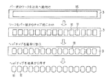
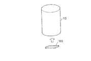
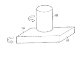
しかし、薄膜磁気ヘッド100に対してブレンド加工を施すためには、図12に示すように、ヘッド加工工程の最終工程において、薄膜磁気ヘッド100を1個ずつ治具113にクランプし、図13に示すように、研磨シート114が貼り付けられた回転基台115に摺接することにより加工を施していた。そのため、生産性が非常に悪いという欠点があった。また、薄膜磁気ヘッド100は、治具113にクランプされる際、ハンドリングされるが、このハンドリングにより、欠け傷などの不良を誘発し、歩留まりを低下させる要因にもなっていた。
【0013】
また、薄膜磁気ヘッド100のパターン形状外周部分のみを面取りするため、薄膜磁気ヘッド100の浮上をコントロールするためのABS面デザインも制約を受けるという欠点もあった。さらに、ブレンド加工中に研磨シート114がABS面に接触する場合があり、ABS面の保護膜としてコーディングされたダイヤモンドライクカーボン(DLC)膜が剥離し、薄膜磁気ヘッド100の信頼性が損なわれるという欠点もあった。
【0014】
さらに、加工条件的にも寸法コントロールが難しく、加工時間が長くかかり、また、薄膜磁気ヘッド100の加工装置の構成が複雑になるなどの欠点もあった。
【0015】
そこで、本発明は、上述した課題を解決するために、ブレンド加工を施すに際して、加工工程が簡略化され、生産効率の改善を図る薄膜磁気ヘッドの研磨装置及び研磨方法を提供することを目的とする。
【0016】
【課題を解決するための手段】
上述した目的を達成するために、本発明に係る研磨装置は、所定間隔に配列された略矩形状のヘッドチップを保持する保持部材と、上記ヘッドチップと対向配置され、上記ヘッドチップのコーナ部が突き当てられて摺動されることにより該ヘッドチップの各コーナー部を研磨する研磨テープと、上記研磨テープを上記所定間隔に配列された任意の2つのヘッドチップの対向するコーナ部に当接させるように、上記ヘッドチップ間に張り出すようにガイドするガイド部材と、上記ガイド部材を上記ヘッドチップの配列方向に揺動させる第1の揺動機構と、上記保持部材を上記ヘッドチップの配列方向と直交する方向に揺動させる第2の揺動機構とを備え、上記ガイド部材は、該第1の揺動機構により上記ヘッドチップの配列方向に揺動され、かつ、上記保持部材は、該第2の揺動機構により上記ヘッドチップの配列方向と直交する方向に揺動されることにより、上記所定間隔に配設された各ヘッドチップのコーナ部を上記研磨テープに摺動させることを特徴とするものである。
【0017】
また、本発明に係る研磨方法は、所定間隔に配列された略矩形状のヘッドチップを保持する保持部材を、上記ヘッドチップと対向配置された研磨テープ側に近接させて、ガイド部材により上記ヘッドチップ側に張り出された上記研磨テープに対して上記ヘッドチップのコーナ部を当接させる工程と、上記ガイド部材を上記ヘッドチップの配列方向に揺動させ、かつ上記保持部材を上記ヘッドチップの配列方向と直交する方向に揺動させることにより上記ヘッドチップの各コーナ部を上記研磨テープと摺動させて研磨する工程とを有し、上記配列されたヘッドチップの各コーナ部を順次研磨するものである。
【0018】
【発明の実施の形態】
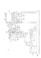
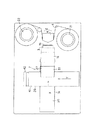
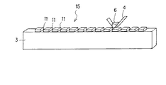
以下、本発明が適用された研磨装置及び研磨方法について、図面を参照しながら詳細に説明する。本発明が適用された研磨装置1は、図1及び図2に示すように、薄膜磁気ヘッドのヘッドチップが所定間隔を隔てて配列されたワークを保持する治具3と、治具3に保持されたワークの研磨を行う研磨テープ4と、この研磨テープを送る送り機構5と、研磨テープ4をワーク側に張り出すようにガイドするガイド部材6と、治具3を移動させる移動機構7とを備える。
【0019】
この研磨装置1は、薄膜磁気ヘッド10の製造工程において、略矩形板状に形成されたヘッドチップ11の各コーナー部に面取り加工を施すために用いられる。この薄膜磁気ヘッド10は、図3に示すように、ヘッドチップ11のハードディスク上を浮上するエアーベアリングサーフェイス(ABS面)11aに所要形状のスライダーパターン12が形成され、ヘッドチップ11の一端面11b側にMRヘッドやインダクティブ型ヘッド等のヘッド素子13が形成されている。そして、薄膜磁気ヘッド10は、ABS面11aの各コーナー部14a〜14dに面取り加工が施されている。
【0020】
このような薄膜磁気ヘッド10に面取り加工を施す研磨装置1は、図4に示すように、複数個のヘッドチップ11が一列に配列されたバー状のワーク15に対して、面取り加工を施すコーナ部を研磨テープ4に摺接させ、円孤面形状に研削する。この研磨装置1によれば、ワーク15に配列されている複数個のヘッドチップ11の面取り加工を順次行うことができる利点があり、生産効率が高く、さらにコーナー部の円孤面形状の寸法コントロールも容易に行え、各薄膜磁気ヘッド10における寸法のばらつきも最小限に抑えることができ、均一な製品を得ることができる。
【0021】
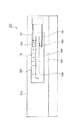
ヘッドチップ11が複数配列されたワーク15を保持する治具3は、略矩形状に形成されたワーク15と略同一の大きさの保持部を有し、ワーク15を保持可能に形成されている。この治具3は治具ホルダ16に固着されている。治具ホルダ16は、治具3を研磨テープ4に対して傾斜して固着することにより、治具3に保持されたワーク15を研磨テープ4に対して傾斜して当接させる。これにより、ヘッドチップ11はコーナー部14を研磨テープ4に当接させることができる。
【0022】
また、治具ホルダ16は、治具3を揺動させる揺動部17が形成されている。揺動部17は、治具ホルダ16の一側面と当接し、偏心して回転される偏心ローラ18と、偏心ローラ18を回転駆動するパルスモータ19とを有する。そして、治具ホルダ16は、パルスモータ19によって偏心ローラ18が回転されることにより、図1中矢印D方向又は反矢印D方向に例えば約±10°揺動される。これにより、治具3に保持されたワーク15のヘッドチップ11と研磨テープ4との当接角度が変えられ、R面形状に加工されるとともに、効率よく面取り加工することができる。
【0023】
この治具ホルダ16は、後述する移動機構7に取り付けられている。治具ホルダ16は、移動機構7により研磨テープ4に対して接離方向に亘って移動されることにより、治具3に保持されたヘッドチップ11の各コーナ部14a〜14dを研磨テープ4に当接させ、またワーク15の交換が行われる。また治具ホルダ16は、移動機構7により研磨テープ4の短手方向に亘って移動されることにより、ヘッドチップ11の面取り加工が行われる。さらに治具ホルダ16は、移動機構7によりヘッドチップ11の配列方向に亘って移動されることにより、ワーク15に配列された各ヘッドチップ11に順次研磨テープ4による面取り加工を施す。
【0024】
このヘッドチップ11に面取り加工を施す研磨テープ4は、ヘッドチップ11のリーディング側あるいはトレーディング側に用いられている材料や、粗加工あるいは仕上加工に応じてテープの種類や番手等を使い分けることができる。
【0025】
この研磨テープ4は、供給リール21から巻取りリール22に亘って巻回されている。供給リール21及び巻取りリール22は、詳細を省略するインジェクションモータ23により駆動され、研磨テープ4を供給リール21及び巻取りリール22間に亘って走行させる。供給リール21及び巻取りリール22の間には治具3が配設されており、研磨テープ4は、供給リール21から繰り出され、ヘッドチップ11の面取り加工を行った後、巻取りリール22に巻取られる。なお、研磨テープ4の巻取り量は、インジェクションモータ23の動作時間をタイマー設定することにより調整することができる。
【0026】
供給リール21と巻取りリール22間には、研磨テープ4を挟んで治具3と相対向する位置に研磨テープ4をワーク15側に張り出すようにガイドするガイド部材6が配設されている。ガイド部材6は、治具3と対向する側が角形に形成され、研磨テープ4を治具3側に張り出すようにガイドしている。そしてガイド部材6は、治具3が移動機構7により研磨テープ4側に近接されることにより、ワーク15の各ヘッドチップ11間に張出しの頂部が位置される。これにより、ガイド部材6は、各ヘッドチップ11のコーナー部14を研磨テープ4に当接させることができる。ガイド部材6は、張出しの頂部の角度が異なる他のガイド部材に交換することにより、ヘッドチップ11の面取りする角度や量を調整することができる。
【0027】
また、このガイド部材6は、パルスモータ24により揺動可能に形成されている。ガイド部材6は、パルスモータ24によって図2中矢印E方向又は反矢印E方向に例えば±約30°揺動される。これにより、研磨テープ4とヘッドチップ11のコーナ部14との当接角度が変えられ、R面形状に加工されるとともに、治具3に保持されたワーク15のヘッドチップ11を効率よく面取り加工することができる。
【0028】
研磨テープ4に対して治具ホルダ16を移動させる移動機構7は、治具ホルダ16を研磨テープ4に対して近接離間させる接離ガイド部25と、治具ホルダ16をワーク15のヘッドチップ11の配列方向に亘って移動させることによりヘッドチップ11を送る送りガイド部26と、治具ホルダ16を研磨テープ4の短手方向に亘って移動させることにより面取り加工を行う加工ガイド部27とを有する。
【0029】
移動機構7は、ガイド部材6に向かって前後に駆動される接離ガイド部25を設け、接離ガイド部25上をヘッドチップ11の配列方向に向かって左右に駆動される送りガイド部26が形成され、さらに、送りガイド部26の上を研磨テープの短手方向に亘って上下に駆動される加工ガイド部27が形成されている。
【0030】
接離ガイド部25は、研磨装置1の基台30に載置されたパルスモータ31により移動体32が研磨テープ4側に向かう図1及び図2中矢印X方向又は反矢印X方向に駆動される。このパルスモータ31は、詳細を省略するシーケンサーで制御され設定されたパルス数だけ図1中矢印X方向又は反矢印X方向に移動することができ、また、移動速度も同様にシーケンサーにて設定できる。移動体32にはパルスモータ31上を移動する移動板33が形成されている。移動板33は、送りガイド部26が設置されている。そして、接離ガイド部25は、パルスモータ31によって移動体32が図1及び図2中矢印X方向又は反矢印X方向に移動されると、移動板33に設置された送りガイド部26とこの送りガイド部26及び加工ガイド部27を介して結合された治具ホルダ16を図1及び図2中矢印X方向又は反矢印X方向に移動させ、ワーク15に配列されたヘッドチップ11を研磨テープ4に近接離間させる。
【0031】
ヘッドチップ11を配列方向に送る送りガイド部26は、接離ガイド部25の移動板33上に基台40が設置され、この基台40上にパルスモータ41及びこのパルスモータ41により移動される移動体42が形成されている。移動体42にはパルスモータ41上を移動する移動板43が形成されている。移動板43は、加工ガイド部27が設置されている。そして、送りガイド部26は、パルスモータ41によって移動体42が図2中矢印Y方向又は反矢印Y方向に移動されると、移動板43に設置された加工ガイド部27及び加工ガイド部27を介して結合された治具ホルダ16を図2中矢印Y方向又は反矢印Y方向に移動させ、ワーク15に配列されたヘッドチップ11を研磨テープ4に対して配列方向に順次送っていく。
【0032】
ヘッドチップ11を研磨テープ4の短手方向に移動することにより各コーナー部14を研磨テープ4上を摺動させ、面取り加工を施す加工ガイド部27は、送りガイド部26の移動板43上に、研磨テープ4の短手方向と略平行な図1中矢印Z方向又は反矢印Z方向に亘ってガイド板50が立設されている。そして、加工ガイド部27は、ガイド板50に沿ってエアシリンダ51と、このエアシリンダ51により図1中矢印Z方向又は反矢印Z方向に駆動されるピストン52が設けられている。ピストン52にはエアシリンダ51の立設方向に沿って移動する移動板53が形成されている。移動板53は、治具ホルダ16を研磨テープ4に対して接離する前後方向に移動可能に支持する支持部材54が設けられている。そして、加工ガイド部27は、エアシリンダ51によってピストン52が図1中矢印Z方向又は反矢印Z方向に移動されると、ピストン52に設置された移動板43及び支持部材54を介して結合された治具ホルダ16を図1中矢印Z方向又は反矢印Z方向に移動させ、ワーク15に配列されたヘッドチップ11を研磨テープ4の短手方向に亘って摺動させ、面取り加工を行うことができる。
【0033】
この治具ホルダ16の研磨テープ4側への押圧力を制御することにより、加工個所や回数等に応じて最適な押圧力でヘッドチップ11を研磨テープ4へ当接させる支持部材54は、加工ガイド部27の移動板53に設けられた支持板55と、支持板55の一端より研磨テープ4側に延設された延設部56上に移動自在に形成されたローラガイド部57と、ローラガイド部57及びローラガイド部57上に形成された治具ホルダ16の端部を押圧するスプリングバネ58とを有する。
【0034】
この支持部材54は、接離ガイド部25によってヘッドチップ11が研磨テープ4及び研磨テープ4を張り出すガイド部材6に当接されると、ガイド部材6の反力によってローラガイド部57が延設部56上を図1及び図2中反矢印X方向に移動し、スプリングバネ58が収縮する。このスプリングバネ58は、バネ係数を用いることにより収縮量に応じた圧力が予め定められている。従って、支持部材54は、スプリングバネ58の収縮量に応じてヘッドチップ11による研磨テープ4への押圧力を測定することができる。
【0035】
このような移動機構7は、治具ホルダ16にワーク15を保持した治具3が装着される前においては、接離ガイド部25が図1中反矢印X方向に移動され、治具ホルダ16にワーク15を保持した治具3を装脱可能とされている。そして移動機構7は、治具ホルダ16にワーク15を保持した治具3が装着されると、パルスモータ31により接離ガイド部25の移動体32がワーク15のヘッドチップ11を研磨テープ4側に近接させる図1中矢印X方向に移動させる。
【0036】
このとき、送りガイド部26は、ワーク15に所定間隔で配列されたヘッドチップ間の略中央にガイド部材6の頂部が位置するように初期設定されているため、相隣接するヘッドチップ11の各コーナ部14の加工精度をほぼ同じくすることができる。そして、移動機構7は、加工ガイド部27によりヘッドチップ11を研磨テープ4の短手方向の下端部に当接させる。
【0037】
ヘッドチップ11と研磨テープ4及び研磨テープ4をワーク15側に張り出すガイド部材6とが当接されると、ガイド部材6からの反力を受けて、支持部材54のスプリングバネ58が収縮する。移動機構7は、スプリングバネ58の収縮量からヘッドチップ11による研磨テープ4への押圧力を測定し、ヘッドチップの研磨個所や粗研磨又は仕上げ研磨等に応じた所定の押圧力にてヘッドチップ11を研磨テープ4に当接させる。
【0038】
次いで、移動機構7は、加工ガイド部27によりワーク15を図1中矢印Z方向に亘って研磨テープ4に摺動させてヘッドチップ11のコーナー部14の面取り加工を行う。このとき、治具ホルダ16を揺動部17によって揺動させるとともに、ガイド部材6をパルスモータ24により揺動させることにより、研磨テープ4とヘッドチップ11のコーナ部14との当接角度が変えられ、治具3に保持されたワーク15のヘッドチップ11を効率よく面取り加工することができる。
【0039】
移動機構7は、加工ガイド部27によりワーク15が研磨テープ4の上端部まで摺動されると、接離ガイド部25によってワーク15を研磨テープ4より退避させる図1中反矢印X方向に移動させる。また、移動機構7は、加工ガイド部27によってワーク15を研磨テープ4の上端から下端まで移動させる。さらに、移動機構7は、送りガイド部26によりワーク15を図2中矢印Y方向に送り、隣のヘッドチップ11間にガイド部材6の頂部を位置させる。なお、このとき研磨テープ4は、インジェクションモータ23によって巻取りリール22側に送られ、新たな研磨面が現れる。
【0040】
次いで、移動機構7は、当該隣のヘッドチップ11の面取り加工に移る。そして、移動機構7は、ワーク15に配列された全てのヘッドチップ11の面取り加工が終了すると、接離ガイド部25及び送りガイド部26を、それぞれ図2中反矢印X方向又は反矢印Y方向に移動させ、治具3よりワーク15を外し、新たなワーク15が取り付けられる。
【0041】
以上のような研磨装置1によれば、ヘッドチップ11が複数配列されたワーク15を移動機構7によって順次移動させ、ヘッドチップ11及びガイド部材6を揺動させながら研磨テープ4によって面取り加工を順次施していく。従って、この研磨装置1は、ワーク15の加工が効率よく行われることにより、ヘッドチップ11の生産効率を上げることができる。また、各ヘッドチップ11の面取り加工を均一に行うことができ、均一な薄膜磁気ヘッド1を供給することができる。
【0042】
そして、この研磨装置1によって形成された薄膜磁気ヘッド10によれば、基板のABS面11aの各コーナー部14a〜14dを面取り形状に加工することにより、ハードディスク6に対する耐衝撃性が著しく向上される。すなわち、ハードディスク6に対して傷が発生したときのG(重力加速度)が、面取り加工を施す前の180Gから250Gへと改善された。
【0043】
また、本発明が適用された研磨装置1によれば、薄膜磁気ヘッド1のコーナー部14のみを研磨テープ4に当てて所要の円弧面形状に加工するため、加工中に研磨テープ4やガイド部材6がABS面11aに触れるおそれがなく、ABS面11aに保護膜として成膜されているDLC膜が剥離することを防止することができる。
【0044】
なお、上述した研磨装置1においては、ヘッドチップ11のコーナー部14のみの面取り加工を施したが、本発明はこれに限らず、ヘッドチップ11の各コーナー部からABS面11aの長手方向及び短手方向に沿って面取りしてもよい。これにより薄膜磁気ヘッド1は、ABS面11aの各コーナー部14a〜14d及び稜線部分に面取り加工を施すことで、ハードディスク6に対する耐衝撃性がさらに向上される。
【0045】
次いで、上述した研磨装置1を用いたヘッドチップ11の研磨方法について説明する。
【0046】
先ず、ワーク15の形成工程について説明する。ワーク15は、所定の工程を経ることにより、図5に示すように、再生専用の磁気抵抗効果型ヘッドと記録専用のインダクティブ型ヘッドとを一体に積層形成してなる複合型の薄膜磁気ヘッド10となる。
【0047】
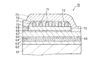
磁気抵抗効果型ヘッドは、磁気抵抗効果素子がハードディスク6に相対するABS面11a側に配置され、且つ一方の端面がハードディスク6に対して露出するように構成される。具体的には、アルチック(Al2O3TiC)等からなる基板61上にアルミナ(Al2O3)等の軟磁性膜による下層シールド62が形成され下部磁性磁極を構成している。この下層シールド62の上に下層ギャップ膜63を介して磁気抵抗効果64を配置している。この磁気抵抗効果素子64の後方には磁気抵抗効果素子64の段着を埋めるAl2O3等からなる絶縁膜65が埋め込まれている。
【0048】
これらの磁気抵抗効果素子64上には、上層ギャップ66を介して軟磁性膜による中間シールド67が設けられている。この中間シールド67が上部磁性磁極を構成しており、下層ギャップ膜63及び上層ギャップ膜66により、磁気抵抗効果型ヘッドのギャップが形成されている。
【0049】
一方、インダクティブ型ヘッドは、軟磁性膜からなり、磁気抵抗効果型ヘッドを構成する中間シールド67を下層磁性コアとして、この中間シールド67上に、SiO2又はAl2O3等からなる記録ギャップ膜68を有する。この記録ギャップ膜68上のハードディスク6に相対する先端側には、磁性膜からなる上層ポール69が形成されている。この上層ポール69の後方には、絶縁層70が埋め込まれて表面が平坦化されている。この平坦化された面上に導体からなるコイル71が形成され、このコイル71を覆って絶縁膜72が形成されている。このコイル71は、図示しないが平面形状がスパイラル状に形成される。そして、このコイル71を用いて、インダクディブ型ヘッドに電磁変換作用によって信号を供給する。
【0050】
さらに絶縁膜72の上方に、上層ポール69に接続して磁性膜から成る上層コア(バックヨーク)73が形成されている。上層ポール69と上層コア73により上部磁性コアが形成されている。上層コア73は、後方においては中間シールド67と接続されて磁路を構成している。このワーク15は、真空薄膜形成技術により形成されるため、狭トラック化や狭ギャップ化等の微細加工が容易で、高分解能記録再生が可能で、高密度磁気記録に対応した薄膜磁気ヘッド10となる。
【0051】
このように構成されるワーク15は、図6に示すように、真空薄膜形成技術により略バー状に形成された後、治具3に取り付けられ、所定間隔毎にスライスされることにより、複数のヘッドチップ11が形成される。そして、ワーク15は、治具3が所定の初期位置に待機している研磨装置1の治具ホルダ16に装着され、各ヘッドチップ11の面取り加工がされる。その後、各ヘッドチップ11は、治具3から取り外される。以下に、ヘッドチップ11の面取り加工工程について説明する。
【0052】
研磨装置1は、治具ホルダ16にワーク15を保持した治具3が装着される前においては、移動機構7の接離ガイド部25が図1中反矢印X方向に移動され、治具ホルダ16にワーク15を保持した治具3を装脱可能とされている。また、研磨装置1は、研磨テープ4が供給リール21及び巻取りリール22間に亘って巻回されるとともに、ガイド部材6により治具ホルダ16側に張り出すようにガイドされている。そして、研磨装置1は、治具ホルダ16にワーク15を保持した治具3が装着される。このとき、各ヘッドチップ11は、研磨テープ4に対して傾斜して装着されるため、コーナー部14を研磨テープ4に当接させることができる。
【0053】
研磨装置1は、治具3が装着されると、移動機構7の接離ガイド部25のパルスモータ31により移動体32をワーク15のヘッドチップ11を研磨テープ4側に近接させる図1中矢印X方向に移動させる。また、研磨装置1は、移動機構7の送りガイド部26によりワーク15に所定間隔で配列されたヘッドチップ11間の略中央にガイド部材6の頂部を位置する。従って、ガイド部材6の頂部を介して左右に位置するヘッドチップ11のコーナー部14を均等に面取り加工することができる。また、研磨装置1は、移動機構7の加工ガイド部27によりヘッドチップ11を研磨テープ4の短手方向の下端部に当接させる。
【0054】
また、研磨装置1は、ヘッドチップ11のコーナー部14と研磨テープ14とが当接されると、ガイド部材6からの反力を受けて、治具ホルダ16がローラガイド部57を介して図1中反矢印X方向に後退し、支持部材54のスプリングバネ58が収縮する。研磨装置1は、このスプリングバネ58の収縮による所定の押圧力によってヘッドチップ11を研磨テープ4に当接させる。
【0055】
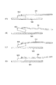
次いで、研磨装置1は、加工ガイド部27によりワーク15を図1中矢印Z方向に移動させてヘッドチップ11を研磨テープ4に摺動させてコーナー部14の面取り加工を行う。このとき、研磨装置1は、図7に示すように、治具ホルダ16を揺動部17によって揺動させるとともに、図8に示すように、ガイド部材6をパルスモータ23により揺動させることにより、研磨テープ4とヘッドチップ11のコーナ部14との当接角度が変えられ、R面形状に加工されるとともに、治具3に保持されたワーク15のヘッドチップ11を効率よく面取り加工することができる。
【0056】
そして加工ガイド部27によりワーク15が研磨テープ4の上端部まで摺動されると、研磨装置1は、接離ガイド部25によってワーク15を研磨テープ4より退避させる図1中反矢印X方向に移動させる。また、研磨装置1は、加工ガイド部27によってワーク15を研磨テープ4の上端から下端まで移動させる。さらに、研磨装置1は、送りガイド部26によりワーク15を図2中矢印Y方向に送り、隣のヘッドチップ11間にガイド部材6の頂部を位置させる。また、研磨装置1は、インジェクションモータ23によって研磨テープ4を巻取りリール22に巻取らせ、供給リール21より新たな研磨面を送り出す。
【0057】
次いで、研磨装置1は、新たにガイド部材6の頂部と相対向する位置に送られたヘッドチップ11間の面取り加工に移る。すなわち、研磨装置1は、移動機構7によりヘッドチップ11を研磨テープ4に摺動させるとともに、治具ホルダ16及びガイド部材16を揺動させる。研磨装置1は、これを繰り返してワーク15に配列されたヘッドチップ11の面取り加工が終了すると、接離ガイド部25及び送りガイド部26を、それぞれ図2中反矢印X方向あるいは反矢印Y方向に移動させ、治具ホルダ16より治具3を外し、ワーク15を反対にしてから治具3を再度治具ホルダ16に取り付け、ヘッドチップ11の他方のコーナー部14の面取り加工を行う。
【0058】
なお、面取り加工においては、ヘッドチップ11の構造上、アルミナ膜とアルチック材が混在するトレーディング側と、アルチック材単体からなるリーディング側においては、それぞれ加工条件を変える必要がある。
【0059】
すなわち、トレーディング側ではアルミナ膜が脆く欠け易いことから、番手の細かい研磨テープ4を選択する。粗加工においては、研磨性の高いダイヤモンドテープを使用し、欠け防止の目的で番手は#4000、接離ガイド部25によるヘッドチップ11と研磨テープ4との押圧力も、突き当て量を50μmと小さめに設定している。その後の仕上げ加工においては、さらに細かいダイヤモンドテープの#8000を使用し、接離ガイド部25の突き当て量は100μmとしている。
【0060】
一方、リーディング側では、粗加工においては、研磨性を重視してWA#1000を使用し、加工回数も3回行う。その後の仕上げ加工においては、粗加工面がかなり粗くなっていることから、ダイヤモンドテープの#8000を使用して、加工回数も3回行う。
【0061】
以上のように、研磨装置1を用いた研磨方法によれば、ワーク15を治具3に保持し、このワーク15の複数配列されたヘッドチップ11の各コーナー部14をヘッドチップ11及びガイド部材6を揺動させながら順次、面取りしていくことができる。従って、ワーク15毎に一括して複数のヘッドチップ11の面取り加工を行うことができ、ヘッドチップ11の生産性を格段に向上させることができる。
【0062】
また、各ヘッドチップ11毎の面取り加工も均一に行うことができ、均一な薄膜磁気ヘッド1を生産することができる。
【0063】
さらに、治具ホルダ16を揺動部17によって揺動させるとともに、ガイド部材6をパルスモータ24により揺動させることにより、研磨テープ4とヘッドチップ11のコーナ部14との当接角度が変えられ、治具3に保持されたワーク15のヘッドチップ11を効率よく面取り加工することができる。
【0064】
そして、この研磨方法によって形成された薄膜磁気ヘッド10によれば、基板のABS面11aの各コーナー部14a〜14dを面取り形状に加工することにより、ハードディスク6に対する耐衝撃性が著しく向上される。すなわち、ハードディスク6に対して傷が発生したときのG(重力加速度)が、面取り加工を施す前の180Gから250Gへと改善された。
【0065】
また、本発明が適用された研磨方法によれば、薄膜磁気ヘッド1のコーナー部14のみを研磨テープ4に当てて所要の円弧面形状に加工するため、加工中に研磨テープ4やガイド部材6がABS面11aに触れるおそれがなく、ABS面11aに保護膜として成膜されているDLC膜が剥離することを防止することができる。
【0066】
なお、上述した研磨方法においては、ヘッドチップ11のコーナー部14のみの面取り加工を施したが、本発明はこれに限らず、ヘッドチップ11の各コーナー部からABS面11aの長手方向及び短手方向に沿って面取りしてもよい。これにより薄膜磁気ヘッド1は、ABS面11aの各コーナー部14a〜14d及び稜線部分に面取り加工を施すことで、ハードディスク6に対する耐衝撃性がさらに向上される。
【0067】
【発明の効果】
以上詳細に説明したように、本発明に係る研磨装置及び研磨方法によれば、ヘッドチップを移動機構によって順次移動させ、揺動機構によってヘッドチップ及びガイド部材を揺動させながら研磨テープによって面取り加工を順次施していく。従って、この研磨装置及び研磨方法によれば、ヘッドチップの加工が効率よく行われることにより、ヘッドチップの生産効率を上げることができる。また、各ヘッドチップの面取り加工を均一に行うことができ、均一な薄膜磁気ヘッドを供給することができる。
【図面の簡単な説明】
【図1】本発明が適用された研磨装置を示す側面図である。
【図2】本発明が適用された研磨装置を示す上面図である。
【図3】薄膜磁気ヘッドを示す斜視図である。
【図4】ヘッドチップが複数配列されたワークを示す図である。
【図5】ワークを示す断面図である。
【図6】ワークの加工工程を示す図である。
【図7】治具ホルダを揺動させながら面取り加工を行う様子を示す図である。
【図8】ガイド部材を揺動させながら面取り加工を行う様子を示す図である。
【図9】薄膜磁気ヘッドとハードディスクとの配置関係を示す斜視図である。
【図10】ハードディスクドライブ装置の概略図である。
【図11】薄膜磁気ヘッドとハードディスクの接触関係を示す図である。
【図12】従来の薄膜磁気ヘッドの加工工程を示す図であり、ヘッドチップを加工治具にクランプする状態を示す図である。
【図13】従来の薄膜磁気ヘッドの加工工程を示す図であり、ヘッドチップを研磨する状態を示す図である。
【符号の説明】
1 研磨装置、3 治具、4 研磨テープ、6 ガイド部材、7 移動機構、10 薄膜磁気ヘッド、11 ヘッドチップ、11a ABS面、14 コーナー部、15 ワーク、16 治具ホルダ、17 揺動部、18 偏心ローラ、19パルスモータ、21 供給リール、22 巻取りリール、[0001]
TECHNICAL FIELD OF THE INVENTION
The present invention relates to a magnetic head constituting a floating type head provided in, for example, a hard disk drive (HDD), and more particularly, to a polishing apparatus and a polishing method for a head chip.
[0002]
[Prior art]
2. Description of the Related Art A hard disk drive (HDD) is provided with a floating magnetic head that floats a head at a small interval with respect to the disk surface of a hard disk (HD) as a recording medium. In order to reduce the size of the head and achieve a high density, a thin-film magnetic head is used in which a head element, a magnetic material serving as a core, and a coil are formed by the same method as a process for manufacturing a semiconductor. As shown in FIG. 9, the thin-film
[0003]
As shown in FIG. 10, a removable hard disk drive device 103 (hereinafter, referred to as a removable HDD device) as a hard disk drive (HDD) on which the thin-film
[0004]
When an external impact is applied to the
[0005]
At this time, the
[0006]
Further, even when the
[0007]
And since the hard disk drive (HDD) is a complicated and precise machine, it is very sensitive to external shocks and vibrations. In particular, the hard disk drive (HDD) and the hard disk drive (HDD) are mounted. If the dropped device falls or is vibrated, a phenomenon occurs in which a magnetic head called a head strap bounces over the surface of the
[0008]
As shown in FIG. 11A, when an impact is applied while the thin-film
[0009]
Therefore, data recorded on the
[0010]
The thin-film
[0011]
Therefore, in order to improve the shock resistance of the thin-film
[0012]
[Problems to be solved by the invention]
However, in order to perform the blending process on the thin-film
[0013]
Further, since only the outer peripheral portion of the pattern shape of the thin-film
[0014]
Further, there are also disadvantages such as difficulty in controlling the dimensions in terms of processing conditions, a long processing time, and a complicated configuration of a processing apparatus for the thin-film
[0015]
Therefore, an object of the present invention is to provide a polishing apparatus and a polishing method for a thin-film magnetic head, in which a processing step is simplified and a production efficiency is improved in performing a blending process in order to solve the above-mentioned problem. I do.
[0016]
[Means for Solving the Problems]
In order to achieve the above-described object, a polishing apparatus according to the present invention includes a holding member that holds substantially rectangular head chips arranged at a predetermined interval, and a facing member that is arranged to face the head chip, and a corner portion of the head chip. The polishing tape is used to polish each corner of the head chip by being abutted and slid, and the polishing tape is brought into contact with opposing corners of any two head chips arranged at the predetermined interval. A guide member for guiding the head chip so as to protrude between the head chips, a first swing mechanism for swinging the guide member in the arrangement direction of the head chips, and an arrangement of the head chips for the holding member. A second swinging mechanism for swinging in a direction perpendicular to the direction, wherein the guide member is swung in the arrangement direction of the head chips by the first swinging mechanism. The holding member is oscillated by the second oscillating mechanism in a direction perpendicular to the direction in which the head chips are arranged, so that the corners of the head chips arranged at the predetermined intervals are polished with the polishing tape. It is characterized in that it is slid in the direction.
[0017]
Further, the polishing method according to the present invention is characterized in that the holding member holding the substantially rectangular head chips arranged at a predetermined interval is brought close to the polishing tape side arranged opposite to the head chip, and the head is moved by the guide member. Contacting the corner portion of the head chip with the polishing tape protruding to the chip side, swinging the guide member in the direction in which the head chips are arranged, and moving the holding member of the head chip. Sliding each corner of the head chip with the polishing tape by oscillating in a direction perpendicular to the arrangement direction, and polishing the head chips, and sequentially polishing each corner of the arranged head chips. Things.
[0018]
BEST MODE FOR CARRYING OUT THE INVENTION
Hereinafter, a polishing apparatus and a polishing method to which the present invention is applied will be described in detail with reference to the drawings. As shown in FIGS. 1 and 2, a
[0019]
The polishing
[0020]
As shown in FIG. 4, a
[0021]
The
[0022]
In addition, the
[0023]
The
[0024]
The polishing
[0025]
The polishing
[0026]
A
[0027]
The
[0028]
The moving
[0029]
The moving
[0030]
The moving
[0031]
The
[0032]
By moving the
[0033]
By controlling the pressing force of the
[0034]
When the
[0035]
Before the
[0036]
At this time, since the
[0037]
When the
[0038]
Next, the moving
[0039]
When the
[0040]
Next, the moving
[0041]
According to the
[0042]
According to the thin-film
[0043]
According to the
[0044]
In the
[0045]
Next, a method of polishing the
[0046]
First, a process of forming the
[0047]
The magnetoresistive head is configured such that the magnetoresistive element is arranged on the ABS 11a side facing the
[0048]
An
[0049]
On the other hand, the inductive head is made of a soft magnetic film, and the
[0050]
Further, an upper core (back yoke) 73 made of a magnetic film is formed above the insulating
[0051]
As shown in FIG. 6, the
[0052]
In the
[0053]
When the
[0054]
When the corner 14 of the
[0055]
Next, the polishing
[0056]
When the
[0057]
Next, the polishing
[0058]
In the chamfering process, due to the structure of the
[0059]
That is, since the alumina film is brittle and easily chipped on the trading side, the polishing
[0060]
On the other hand, on the leading side, in rough processing, WA # 1000 is used with emphasis on abrasiveness, and the number of times of processing is also three. In the subsequent finishing, since the roughened surface is considerably rough, the number of workings is also three times using diamond tape # 8000.
[0061]
As described above, according to the polishing method using the
[0062]
Further, chamfering for each
[0063]
Further, the contact angle between the polishing
[0064]
According to the thin-film
[0065]
Further, according to the polishing method to which the present invention is applied, only the corner portion 14 of the thin-film
[0066]
In the above-described polishing method, the chamfering process is performed only on the corner portion 14 of the
[0067]
【The invention's effect】
As described in detail above, according to the polishing apparatus and the polishing method according to the present invention, the head chip is sequentially moved by the moving mechanism, and the head chip and the guide member are rocked by the rocking mechanism, and chamfering is performed by the polishing tape. Is applied sequentially. Therefore, according to the polishing apparatus and the polishing method, the head chips can be efficiently processed, so that the production efficiency of the head chips can be increased. Further, chamfering of each head chip can be performed uniformly, and a uniform thin-film magnetic head can be supplied.
[Brief description of the drawings]
FIG. 1 is a side view showing a polishing apparatus to which the present invention is applied.
FIG. 2 is a top view showing a polishing apparatus to which the present invention is applied.
FIG. 3 is a perspective view showing a thin-film magnetic head.
FIG. 4 is a diagram showing a work in which a plurality of head chips are arranged.
FIG. 5 is a sectional view showing a work.
FIG. 6 is a view showing a processing step of a work.
FIG. 7 is a diagram showing a state in which chamfering is performed while swinging the jig holder.
FIG. 8 is a diagram illustrating a state in which chamfering is performed while swinging a guide member.
FIG. 9 is a perspective view showing an arrangement relationship between a thin-film magnetic head and a hard disk.
FIG. 10 is a schematic diagram of a hard disk drive.
FIG. 11 is a diagram showing a contact relationship between a thin-film magnetic head and a hard disk.
FIG. 12 is a view showing a processing step of a conventional thin-film magnetic head, showing a state in which a head chip is clamped to a processing jig.
FIG. 13 is a view showing a processing step of a conventional thin-film magnetic head, showing a state in which a head chip is polished.
[Explanation of symbols]
Claims (6)
上記ヘッドチップと対向配置され、上記ヘッドチップのコーナ部が突き当てられて摺動されることにより該ヘッドチップの各コーナー部を研磨する研磨テープと、
上記研磨テープを上記所定間隔に配列された任意の2つのヘッドチップの対向するコーナ部に当接させるように、上記ヘッドチップ間に張り出すようにガイドするガイド部材と、
上記ガイド部材を上記ヘッドチップの配列方向に揺動させる第1の揺動機構と、
上記保持部材を上記ヘッドチップの配列方向と直交する方向に揺動させる第2の揺動機構とを備え、
上記ガイド部材は、該第1の揺動機構により上記ヘッドチップの配列方向に揺動され、
かつ、上記保持部材は、該第2の揺動機構により上記ヘッドチップの配列方向と直交する方向に揺動されることにより、
上記所定間隔に配設された各ヘッドチップのコーナ部を上記研磨テープに摺動させることを特徴とする研磨装置。A holding member for holding substantially rectangular head chips arranged at predetermined intervals,
A polishing tape that is arranged to face the head chip, and polishes each corner of the head chip by being slid against the corner of the head chip,
A guide member that guides the polishing tape so as to project between the head chips so that the polishing tape abuts on opposing corner portions of any two head chips arranged at the predetermined interval.
A first swing mechanism for swinging the guide member in the direction in which the head chips are arranged;
A second swing mechanism for swinging the holding member in a direction orthogonal to the arrangement direction of the head chips,
The guide member is swung by the first swing mechanism in an arrangement direction of the head chips,
The holding member is swung by the second swing mechanism in a direction orthogonal to the arrangement direction of the head chips,
A polishing apparatus, characterized in that corner portions of each head chip arranged at the predetermined interval are slid on the polishing tape.
上記移動機構は、上記保持部材を上記研磨テープの長手方向と直交する短手方向に移動させながら、上記所定間隔に配設された各ヘッドチップのコーナ部を上記研磨テープに摺動させることを特徴とする請求項1記載の研磨装置。A moving mechanism for moving the holding member in a short direction orthogonal to the longitudinal direction of the polishing tape,
The moving mechanism may slide the corners of the head chips disposed at the predetermined intervals on the polishing tape while moving the holding member in a short direction orthogonal to the longitudinal direction of the polishing tape. The polishing apparatus according to claim 1, wherein:
上記研磨テープを送る送り機構とを備え、
一のヘッドチップの研磨が終了すると、上記移動機構は、上記保持部材を上記研磨テープ並びにガイド部材から離す方向、かつ上記所定間隔だけ上記ヘッドチップの配列方向に移動させ、
上記送り機構は、上記研磨テープを長手方向に一定量だけ送ることを特徴とする請求項1又は2記載の研磨装置。A moving mechanism for moving the holding member in the direction of contact and separation with respect to the polishing tape and the guide member and the direction in which the head chips are arranged,
And a feed mechanism for feeding the polishing tape,
When the polishing of one head chip is completed, the moving mechanism moves the holding member in the direction in which the holding member is separated from the polishing tape and the guide member, and in the direction in which the head chips are arranged by the predetermined interval,
3. The polishing apparatus according to claim 1, wherein the feed mechanism feeds the polishing tape by a predetermined amount in the longitudinal direction.
上記ガイド部材を上記ヘッドチップの配列方向に揺動させ、かつ上記保持部材を上記ヘッドチップの配列方向と直交する方向に揺動させることにより上記ヘッドチップの各コーナ部を上記研磨テープと摺動させて研磨する工程とを有し、
上記配列されたヘッドチップの各コーナ部を順次研磨する研磨方法。A holding member for holding substantially rectangular head chips arranged at predetermined intervals is brought close to the polishing tape side arranged opposite to the head chip, and the polishing tape protruded toward the head chip side by a guide member. Abutting the corner of the head chip against
Each corner of the head chip slides with the polishing tape by swinging the guide member in the direction in which the head chips are arranged, and swinging the holding member in a direction orthogonal to the direction in which the head chips are arranged. And polishing step,
A polishing method for sequentially polishing each corner of the arranged head chips.
上記ヘッドチップを上記研磨テープ及びガイド部材から離す方向に移動させる工程と、
上記保持部を上記ヘッドチップの配列方向に上記所定間隔だけ移動させて他のヘッドチップを上記研磨テープと対向させる工程と、
上記研磨テープを長手方向に一定量だけ送る工程とを有することを特徴とする請求項4又は5記載の研磨方法。After polishing of each corner of the one head chip is completed,
A step of moving the head chip in a direction away from the polishing tape and the guide member,
A step of moving the holding portion by the predetermined interval in the direction in which the head chips are arranged so that another head chip faces the polishing tape,
6. The polishing method according to claim 4, further comprising a step of feeding the polishing tape by a predetermined amount in the longitudinal direction.
Priority Applications (1)
| Application Number | Priority Date | Filing Date | Title |
|---|---|---|---|
| JP2002308771A JP2004142003A (en) | 2002-10-23 | 2002-10-23 | Polishing apparatus and polishing method |
Applications Claiming Priority (1)
| Application Number | Priority Date | Filing Date | Title |
|---|---|---|---|
| JP2002308771A JP2004142003A (en) | 2002-10-23 | 2002-10-23 | Polishing apparatus and polishing method |
Publications (1)
| Publication Number | Publication Date |
|---|---|
| JP2004142003A true JP2004142003A (en) | 2004-05-20 |
Family
ID=32454824
Family Applications (1)
| Application Number | Title | Priority Date | Filing Date |
|---|---|---|---|
| JP2002308771A Withdrawn JP2004142003A (en) | 2002-10-23 | 2002-10-23 | Polishing apparatus and polishing method |
Country Status (1)
| Country | Link |
|---|---|
| JP (1) | JP2004142003A (en) |
Cited By (1)
| Publication number | Priority date | Publication date | Assignee | Title |
|---|---|---|---|---|
| US8339742B1 (en) * | 2008-08-19 | 2012-12-25 | Western Digital (Fremont), Llc | Slider with leading edge blend and conformal step features |
-
2002
- 2002-10-23 JP JP2002308771A patent/JP2004142003A/en not_active Withdrawn
Cited By (1)
| Publication number | Priority date | Publication date | Assignee | Title |
|---|---|---|---|---|
| US8339742B1 (en) * | 2008-08-19 | 2012-12-25 | Western Digital (Fremont), Llc | Slider with leading edge blend and conformal step features |
Similar Documents
| Publication | Publication Date | Title |
|---|---|---|
| US5735036A (en) | Lapping process for minimizing shorts and element recession at magnetic head air bearing surface | |
| US5603156A (en) | Lapping process for minimizing shorts and element recession at magnetic head air bearing surface | |
| US5749769A (en) | Lapping process using micro-advancement for optimizing flatness of a magnetic head air bearing surface | |
| JP4685734B2 (en) | Manufacturing method of magnetic head slider | |
| US8146237B2 (en) | Method of manufacturing a magnetic head | |
| US5722156A (en) | Method for processing ceramic wafers comprising plural magnetic head forming units | |
| JP2002331452A (en) | Polishing apparatus, magnetic head, and method of manufacturing the same | |
| JP3990197B2 (en) | Thin film magnetic head | |
| US6997784B2 (en) | Storage device slider with sacrificial lapping extension | |
| JP2008027516A (en) | Manufacturing method of magnetic head slider | |
| JP2004142003A (en) | Polishing apparatus and polishing method | |
| JPH0773425A (en) | Method for manufacturing floating magnetic head device | |
| JP2002237008A (en) | Thin film magnetic head | |
| JP3462023B2 (en) | Method of manufacturing side core type magnetic head slider | |
| JP2009158070A (en) | Manufacturing method of magnetic head slider | |
| JPH09293221A (en) | Magnetic head slider and method of manufacturing the same | |
| CN113963721B (en) | Microwave assisted magnetic recording head slider and grinding method thereof | |
| JP5388586B2 (en) | Manufacturing method of slider having magnetic head | |
| JP2006172691A (en) | Magnetic head manufacturing method, magnetic head, angle setting device, and lapping device head | |
| US20140295740A1 (en) | Ultra fine lapping substrate through use of hard coated material on lapping kinematics | |
| JP4860989B2 (en) | Manufacturing method of head slider | |
| JP2004087056A (en) | Thin film magnetic head and manufacturing method | |
| JP2000293828A (en) | Magnetic head, its production, and device for producing the magnetic head | |
| JP2003141704A (en) | Thin film magnetic head | |
| JP5147467B2 (en) | Manufacturing method of thin film magnetic head |
Legal Events
| Date | Code | Title | Description |
|---|---|---|---|
| A300 | Withdrawal of application because of no request for examination |
Free format text: JAPANESE INTERMEDIATE CODE: A300 Effective date: 20060110 |