JP2004146816A - 固体撮像装置およびこれを用いた機器 - Google Patents
固体撮像装置およびこれを用いた機器 Download PDFInfo
- Publication number
- JP2004146816A JP2004146816A JP2003341358A JP2003341358A JP2004146816A JP 2004146816 A JP2004146816 A JP 2004146816A JP 2003341358 A JP2003341358 A JP 2003341358A JP 2003341358 A JP2003341358 A JP 2003341358A JP 2004146816 A JP2004146816 A JP 2004146816A
- Authority
- JP
- Japan
- Prior art keywords
- semiconductor chip
- imaging device
- image processing
- chip
- solid
- Prior art date
- Legal status (The legal status is an assumption and is not a legal conclusion. Google has not performed a legal analysis and makes no representation as to the accuracy of the status listed.)
- Ceased
Links
Images


Landscapes
- Solid State Image Pick-Up Elements (AREA)
- Transforming Light Signals Into Electric Signals (AREA)
Abstract
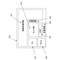
【解決手段】 撮像装置を、センサ部102を含む撮像チップ101と画像処理回路110を含む画像処理チップ106の2チップ構成とし、撮像チップ101の全回路のトランジスタをnMOSもしくはpMOSのいずれか一方のみで構成し、撮像チップ101を画像処理チップ106の上に積層する。
【選択図】 図1
Description
102 センサ部
103 水平走査回路
104 垂直走査回路
105 アンプ
106 画像処理チップ
107 タイミングパルス発生回路
108 ゲイン制御アンプ
109 AD変換回路
110 画像処理回路
111 タイミングパルス出力端子
112 タイミングパルス入力端子
113 映像信号出力端子
114 映像信号入力端子
301 マイク
302 音声符号化部
303 システム制御部
304 通信制御部
305 アンテナ
306 スピーカー
307 表示制御部
308 表示装置
309 撮像装置
310 画像符号化部
401 撮像装置
402 システム制御部
403 画像符号化/復号化部
404 記録メディア制御部
405 記録メディア
406 表示制御部
407 表示装置
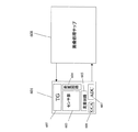
501 1チップCMOSセンサ
502 画像処理回路
503 タイミングパルス発生回路
504 ゲイン制御アンプ
505 AD変換回路
506 垂直走査回路
507 センサ部
508 水平走査回路
601 撮像チップ
602 タイミングパルス発生回路
603 センサ部
604 垂直走査回路
605 水平走査回路
606 ゲイン制御アンプ
607 AD変換回路
608 画像処理チップ
Claims (15)
- 全てのトランジスタが同一導電体のトランジスタで構成された撮像用半導体チップと、
CMOS型のトランジスタで構成された画像処理用半導体チップとを備えたことを特徴とする固体撮像装置。 - 前記撮像用半導体チップが前記画像処理用半導体チップの上に積層された、請求項1に記載の固体撮像装置。
- 前記撮像用半導体チップの全てのトランジスタが、nチャネル型MOSトランジスタで構成された、請求項1に記載の固体撮像装置。
- 前記撮像用半導体チップの全てのトランジスタが、pチャネル型MOSトランジスタで構成された、請求項1に記載の固体撮像装置。
- 前記撮像用半導体チップが、光を電荷に変換する光電変換部と、前記光電変換部で発生した電荷に応じた信号を増幅するアンプとを備えた、請求項1に記載の固体撮像装置。
- 前記撮像用半導体チップと前記画像処理用半導体チップとが、ボンディングワイヤにより電気的に接続された、請求項1に記載の固体撮像装置。
- 前記撮像用半導体チップに貫通電極が形成され、前記貫通電極に接続された配線を介して、前記撮像用半導体チップと前記画像処理用半導体チップとが電気的に接続された、請求項1に記載の固体撮像装置。
- 前記貫通電極がSi貫通電極である、請求項7に記載の固体撮像装置。
- 前記画像処理用半導体チップに、前記撮像用半導体チップへタイミングパルスを供給するタイミングパルス発生回路と、ゲイン制御アンプと、アナログデジタル変換回路とを備えた、請求項1に記載の固体撮像装置。
- 前記画像処理用半導体チップが、タイミングパルスを出力するタイミングパルス出力端子を含む複数の端子を有し、
前記撮像用半導体チップが、前記タイミングパルスが入力されるタイミングパルス入力端子を含む複数の端子を有し、
前記タイミングパルス入力端子と前記タイミングパルス出力端子とが近傍に配置されるように、前記撮像用半導体チップが前記画像処理用半導体チップの上に積層された、請求項2に記載の固体撮像装置。 - 前記撮像用半導体チップが、撮像した映像信号を出力する映像信号出力端子を含む複数の端子を有し、
前記画像処理用半導体チップが、前記映像信号が入力される映像信号入力端子を含む複数の端子を有し、
前記映像信号出力端子と前記映像信号入力端子とが近傍に配置されるように、前記撮像用半導体チップが前記画像処理用半導体チップの上に積層された、請求項2に記載の固体撮像装置。 - 請求項1〜11のいずれか一項に記載の固体撮像装置と、前記固体撮像装置で撮影された静止画もしくは動画を処理する画像処理部とを備えたことを特徴とする機器。
- 携帯電話である請求項12に記載の機器。
- 携帯型情報端末である請求項12に記載の機器。
- デジタルスチルカメラである請求項12に記載の機器。
Priority Applications (1)
| Application Number | Priority Date | Filing Date | Title |
|---|---|---|---|
| JP2003341358A JP2004146816A (ja) | 2002-09-30 | 2003-09-30 | 固体撮像装置およびこれを用いた機器 |
Applications Claiming Priority (2)
| Application Number | Priority Date | Filing Date | Title |
|---|---|---|---|
| JP2002287609 | 2002-09-30 | ||
| JP2003341358A JP2004146816A (ja) | 2002-09-30 | 2003-09-30 | 固体撮像装置およびこれを用いた機器 |
Publications (1)
| Publication Number | Publication Date |
|---|---|
| JP2004146816A true JP2004146816A (ja) | 2004-05-20 |
Family
ID=32473305
Family Applications (1)
| Application Number | Title | Priority Date | Filing Date |
|---|---|---|---|
| JP2003341358A Ceased JP2004146816A (ja) | 2002-09-30 | 2003-09-30 | 固体撮像装置およびこれを用いた機器 |
Country Status (1)
| Country | Link |
|---|---|
| JP (1) | JP2004146816A (ja) |
Cited By (22)
| Publication number | Priority date | Publication date | Assignee | Title |
|---|---|---|---|---|
| WO2006003906A1 (ja) * | 2004-07-01 | 2006-01-12 | Sony Corporation | 撮像装置、撮像素子及び撮像装置の制御方法 |
| JP2006049361A (ja) * | 2004-07-30 | 2006-02-16 | Sony Corp | 半導体モジュール及びmos型固体撮像装置 |
| WO2006080359A1 (ja) * | 2005-01-26 | 2006-08-03 | Matsushita Electric Industrial Co., Ltd. | 撮像装置 |
| JP2007242705A (ja) * | 2006-03-06 | 2007-09-20 | Sanyo Electric Co Ltd | マルチチップパッケージ |
| JP2008034752A (ja) * | 2006-07-31 | 2008-02-14 | Nec Corp | 半導体装置 |
| WO2008023519A1 (en) * | 2006-08-22 | 2008-02-28 | Panasonic Corporation | Imaging apparatus chip set and image pickup system |
| KR100835892B1 (ko) | 2007-03-26 | 2008-06-09 | (주)실리콘화일 | 칩 적층 이미지센서 |
| JP2009094273A (ja) * | 2007-10-09 | 2009-04-30 | Fujifilm Corp | 固体撮像素子、撮像装置、及び固体撮像素子の製造方法 |
| WO2011083722A1 (ja) * | 2010-01-08 | 2011-07-14 | ソニー株式会社 | 半導体装置、固体撮像装置、およびカメラシステム |
| JP2012033894A (ja) * | 2010-06-30 | 2012-02-16 | Canon Inc | 固体撮像装置 |
| EP2426719A2 (en) | 2010-09-03 | 2012-03-07 | Sony Corporation | Semiconductor integrated circuit, electronic device, solid-state imaging apparatus, and imaging apparatus |
| WO2013145753A1 (ja) * | 2012-03-30 | 2013-10-03 | 株式会社ニコン | 撮像素子および撮像装置 |
| JP2014143667A (ja) * | 2012-12-28 | 2014-08-07 | Canon Inc | 撮像素子、撮像装置、その制御方法、および制御プログラム |
| JP2015084424A (ja) * | 2010-01-08 | 2015-04-30 | ソニー株式会社 | 半導体装置、固体撮像装置、およびカメラシステム |
| US9171968B2 (en) | 2012-03-15 | 2015-10-27 | Sony Corporation | Solid-state imaging device and camera system |
| WO2015198876A1 (ja) * | 2014-06-24 | 2015-12-30 | ソニー株式会社 | 撮像素子、電子機器 |
| US9634060B2 (en) | 2012-07-04 | 2017-04-25 | Makoto Shizukuishi | Stacked solid-state image sensor and imaging apparatus including the same |
| WO2018131216A1 (ja) | 2017-01-12 | 2018-07-19 | 三菱電機株式会社 | 赤外線センサ基板及び赤外線センサデバイス |
| US10418394B2 (en) | 2010-06-02 | 2019-09-17 | Sony Corporation | Semiconductor device, solid-state imaging device, and camera system |
| JP2020061755A (ja) * | 2016-09-16 | 2020-04-16 | ソニーセミコンダクタソリューションズ株式会社 | 撮像装置、及び、電子機器 |
| JP2020191467A (ja) * | 2010-06-30 | 2020-11-26 | キヤノン株式会社 | 固体撮像装置 |
| US12622076B2 (en) | 2020-07-03 | 2026-05-05 | Mitsubishi Electric Corporation | Infrared sensor and method of manufacturing infrared sensor |
-
2003
- 2003-09-30 JP JP2003341358A patent/JP2004146816A/ja not_active Ceased
Cited By (57)
| Publication number | Priority date | Publication date | Assignee | Title |
|---|---|---|---|---|
| US7719578B2 (en) | 2004-07-01 | 2010-05-18 | Sony Corporation | Image pickup apparatus, image pickup element, and method for controlling image pickup apparatus |
| JP2006020023A (ja) * | 2004-07-01 | 2006-01-19 | Sony Corp | 撮像装置、撮像素子及び撮像装置の制御方法 |
| WO2006003906A1 (ja) * | 2004-07-01 | 2006-01-12 | Sony Corporation | 撮像装置、撮像素子及び撮像装置の制御方法 |
| JP2006049361A (ja) * | 2004-07-30 | 2006-02-16 | Sony Corp | 半導体モジュール及びmos型固体撮像装置 |
| US8508639B2 (en) | 2004-07-30 | 2013-08-13 | Sony Corporation | Semiconductor module, MOS type solid-state image pickup device, camera and manufacturing method of camera |
| KR101096370B1 (ko) | 2004-07-30 | 2011-12-20 | 소니 주식회사 | 반도체 모듈, mos형 고체 촬상 장치, 카메라 및카메라의 제조 방법 |
| WO2006080359A1 (ja) * | 2005-01-26 | 2006-08-03 | Matsushita Electric Industrial Co., Ltd. | 撮像装置 |
| JP2007242705A (ja) * | 2006-03-06 | 2007-09-20 | Sanyo Electric Co Ltd | マルチチップパッケージ |
| JP2008034752A (ja) * | 2006-07-31 | 2008-02-14 | Nec Corp | 半導体装置 |
| WO2008023519A1 (en) * | 2006-08-22 | 2008-02-28 | Panasonic Corporation | Imaging apparatus chip set and image pickup system |
| KR100835892B1 (ko) | 2007-03-26 | 2008-06-09 | (주)실리콘화일 | 칩 적층 이미지센서 |
| JP2009094273A (ja) * | 2007-10-09 | 2009-04-30 | Fujifilm Corp | 固体撮像素子、撮像装置、及び固体撮像素子の製造方法 |
| US8541730B2 (en) | 2007-10-09 | 2013-09-24 | Fujifilm Corporation | Solid-state imaging device, imaging apparatus, and method for manufacturing solid-state imaging device |
| DE202010018564U1 (de) | 2010-01-08 | 2017-09-07 | Sony Corporation | Halbleitervorrichtung, Festkörper-Bildsensoren und Kamerasystem |
| EP3525237A1 (en) | 2010-01-08 | 2019-08-14 | Sony Corporation | Semiconductor device, solid-state image sensor and camera system |
| EP3528284A2 (en) | 2010-01-08 | 2019-08-21 | Sony Corporation | Semiconductor device, solid-state image sensor and camera system |
| EP3267480A1 (en) | 2010-01-08 | 2018-01-10 | Sony Corporation | Semiconductor device, solid-state image sensor and camera system |
| WO2011083722A1 (ja) * | 2010-01-08 | 2011-07-14 | ソニー株式会社 | 半導体装置、固体撮像装置、およびカメラシステム |
| DE202010018542U1 (de) | 2010-01-08 | 2017-07-27 | Sony Corp. | Halbleitervorrichtung, Festkörper-Bildsensoren und Kamerasystem |
| JP2015084424A (ja) * | 2010-01-08 | 2015-04-30 | ソニー株式会社 | 半導体装置、固体撮像装置、およびカメラシステム |
| US9093363B2 (en) | 2010-01-08 | 2015-07-28 | Sony Corporation | Semiconductor device, solid-state image sensor and camera system for reducing the influence of noise at a connection between chips |
| US9641777B2 (en) | 2010-01-08 | 2017-05-02 | Sony Corporation | Semiconductor device, solid-state image sensor and camera system |
| KR20160106782A (ko) | 2010-01-08 | 2016-09-12 | 소니 주식회사 | 반도체 장치, 고체 촬상 장치, 및 카메라 시스템 |
| KR20160106784A (ko) | 2010-01-08 | 2016-09-12 | 소니 주식회사 | 반도체 장치, 고체 촬상 장치, 및 카메라 시스템 |
| US10418394B2 (en) | 2010-06-02 | 2019-09-17 | Sony Corporation | Semiconductor device, solid-state imaging device, and camera system |
| US11616089B2 (en) | 2010-06-02 | 2023-03-28 | Sony Corporation | Semiconductor device, solid-state imaging device, and camera system |
| JP2022132369A (ja) * | 2010-06-30 | 2022-09-08 | キヤノン株式会社 | 固体撮像装置 |
| JP2020191467A (ja) * | 2010-06-30 | 2020-11-26 | キヤノン株式会社 | 固体撮像装置 |
| US9972650B2 (en) | 2010-06-30 | 2018-05-15 | Canon Kabushiki Kaisha | Solid-state imaging apparatus and method for manufacturing the solid-state imaging apparatus having sealing portion disposed in bonded members |
| US10847558B2 (en) | 2010-06-30 | 2020-11-24 | Canon Kabushiki Kaisha | Solid-state imaging apparatus and method for manufacturing the solid-state imaging apparatus having sealing portion disposed in bonded members |
| JP2012033894A (ja) * | 2010-06-30 | 2012-02-16 | Canon Inc | 固体撮像装置 |
| US9000501B2 (en) | 2010-09-03 | 2015-04-07 | Sony Corporation | Semiconductor integrated circuit, electronic device, solid-state imaging apparatus, and imaging apparatus |
| EP3544057A1 (en) | 2010-09-03 | 2019-09-25 | Sony Corporation | Semiconductor integrated circuit, electronic device, solid-state imaging apparatus, and imaging apparatus |
| EP3483939A1 (en) | 2010-09-03 | 2019-05-15 | Sony Corporation | Semiconductor integrated circuit, electronic device, solid-state imaging apparatus, and imaging apparatus |
| EP2426719A2 (en) | 2010-09-03 | 2012-03-07 | Sony Corporation | Semiconductor integrated circuit, electronic device, solid-state imaging apparatus, and imaging apparatus |
| US9171968B2 (en) | 2012-03-15 | 2015-10-27 | Sony Corporation | Solid-state imaging device and camera system |
| US11689832B2 (en) | 2012-03-30 | 2023-06-27 | Nikon Corporation | Image pickup element and image pickup device |
| US11317046B2 (en) | 2012-03-30 | 2022-04-26 | Nikon Corporation | Image pickup element and image pickup device |
| US10574918B2 (en) | 2012-03-30 | 2020-02-25 | Nikon Corporation | Image pickup element and image pickup device |
| US12432469B2 (en) | 2012-03-30 | 2025-09-30 | Nikon Corporation | Image pickup element and image pickup device |
| US12088943B2 (en) | 2012-03-30 | 2024-09-10 | Nikon Corporation | Image pickup element and image pickup device |
| US10244194B2 (en) | 2012-03-30 | 2019-03-26 | Nikon Corporation | Individual cell charge control in an image sensor |
| WO2013145753A1 (ja) * | 2012-03-30 | 2013-10-03 | 株式会社ニコン | 撮像素子および撮像装置 |
| US9634060B2 (en) | 2012-07-04 | 2017-04-25 | Makoto Shizukuishi | Stacked solid-state image sensor and imaging apparatus including the same |
| JP2014143667A (ja) * | 2012-12-28 | 2014-08-07 | Canon Inc | 撮像素子、撮像装置、その制御方法、および制御プログラム |
| WO2015198876A1 (ja) * | 2014-06-24 | 2015-12-30 | ソニー株式会社 | 撮像素子、電子機器 |
| US12146963B2 (en) | 2016-09-16 | 2024-11-19 | Sony Semiconductor Solutions Corporation | Imaging device and electronic device |
| JP2022111151A (ja) * | 2016-09-16 | 2022-07-29 | ソニーセミコンダクタソリューションズ株式会社 | 撮像装置及び撮像装置の制御方法 |
| JP7342197B2 (ja) | 2016-09-16 | 2023-09-11 | ソニーセミコンダクタソリューションズ株式会社 | 撮像装置及び撮像装置の制御方法 |
| US12061264B2 (en) | 2016-09-16 | 2024-08-13 | Sony Semiconductor Solutions Corporation | Imaging device and electronic device |
| US12130362B2 (en) | 2016-09-16 | 2024-10-29 | Sony Semiconductor Solutions Corporation | Imaging device and electronic device |
| JP7105754B2 (ja) | 2016-09-16 | 2022-07-25 | ソニーセミコンダクタソリューションズ株式会社 | 撮像装置、及び、撮像装置の制御方法 |
| US12306305B2 (en) | 2016-09-16 | 2025-05-20 | Sony Semiconductor Solutions Corporation | Imaging device and electronic device |
| JP2020061755A (ja) * | 2016-09-16 | 2020-04-16 | ソニーセミコンダクタソリューションズ株式会社 | 撮像装置、及び、電子機器 |
| WO2018131216A1 (ja) | 2017-01-12 | 2018-07-19 | 三菱電機株式会社 | 赤外線センサ基板及び赤外線センサデバイス |
| US10847567B2 (en) | 2017-01-12 | 2020-11-24 | Mitsubishi Electric Corporation | Infrared sensor device including infrared sensor substrate and signal processing circuit substrate coupled to each other |
| US12622076B2 (en) | 2020-07-03 | 2026-05-05 | Mitsubishi Electric Corporation | Infrared sensor and method of manufacturing infrared sensor |
Similar Documents
| Publication | Publication Date | Title |
|---|---|---|
| JP2004146816A (ja) | 固体撮像装置およびこれを用いた機器 | |
| US7164113B2 (en) | Solid state imaging device with semiconductor imaging and processing chips | |
| JP5507563B2 (ja) | イメージセンサ | |
| US8558292B2 (en) | Active pixel sensor having two wafers | |
| CN101849408B (zh) | 具有共享处理的多图像传感器系统 | |
| US9426396B2 (en) | Image sensor, image capturing apparatus, and cellular phone for reduced power consumption when performing thinning readout | |
| JP6463944B2 (ja) | 撮像素子、撮像装置及び携帯電話機 | |
| KR102015900B1 (ko) | 고체 촬상 소자 및 촬상 장치 | |
| CN109714551B (zh) | 固体摄像装置、固体摄像装置的驱动方法以及电子设备 | |
| JP2007142738A (ja) | 物理情報取得方法および物理情報取得装置 | |
| JP2011517510A (ja) | 2枚のウエハを有するアクティブ画素センサ | |
| US20120002092A1 (en) | Low noise active pixel sensor | |
| JP2004111572A (ja) | 撮像装置および画像ピックアップシステム | |
| KR101782334B1 (ko) | 촬상 소자, 촬상장치 및 휴대전화기 | |
| JP2008017090A (ja) | 撮像装置、及び電子ズーム方法 | |
| JP2017212564A (ja) | 撮像装置、および制御方法 | |
| JP6494263B2 (ja) | 撮像素子及び電子機器 | |
| JP2005191800A (ja) | 信号出力装置、信号処理装置、固体撮像装置、インタフェース装置、電子機器ならびにインタフェース装置の動作方法 | |
| JP2003258230A (ja) | 半導体装置及び半導体撮像装置 | |
| JP4687383B2 (ja) | 光学系一体型撮像モジュール及びそれを用いた携帯端末 | |
| JP2020014255A (ja) | 撮像素子及び撮像装置 | |
| JP7160129B2 (ja) | 撮像素子および撮像装置 | |
| JP2018057004A (ja) | 撮像素子、撮像装置及び携帯電話機 |
Legal Events
| Date | Code | Title | Description |
|---|---|---|---|
| A621 | Written request for application examination |
Free format text: JAPANESE INTERMEDIATE CODE: A621 Effective date: 20060116 |
|
| A131 | Notification of reasons for refusal |
Free format text: JAPANESE INTERMEDIATE CODE: A131 Effective date: 20090416 |
|
| A977 | Report on retrieval |
Free format text: JAPANESE INTERMEDIATE CODE: A971007 Effective date: 20090416 |
|
| A521 | Request for written amendment filed |
Free format text: JAPANESE INTERMEDIATE CODE: A523 Effective date: 20090610 |
|
| A131 | Notification of reasons for refusal |
Free format text: JAPANESE INTERMEDIATE CODE: A131 Effective date: 20090915 |
|
| A521 | Request for written amendment filed |
Free format text: JAPANESE INTERMEDIATE CODE: A523 Effective date: 20091116 |
|
| A01 | Written decision to grant a patent or to grant a registration (utility model) |
Free format text: JAPANESE INTERMEDIATE CODE: A01 Effective date: 20100126 |
|
| A045 | Written measure of dismissal of application [lapsed due to lack of payment] |
Free format text: JAPANESE INTERMEDIATE CODE: A045 Effective date: 20100520 |