JP2004184663A - Optical module - Google Patents
Optical module Download PDFInfo
- Publication number
- JP2004184663A JP2004184663A JP2002350826A JP2002350826A JP2004184663A JP 2004184663 A JP2004184663 A JP 2004184663A JP 2002350826 A JP2002350826 A JP 2002350826A JP 2002350826 A JP2002350826 A JP 2002350826A JP 2004184663 A JP2004184663 A JP 2004184663A
- Authority
- JP
- Japan
- Prior art keywords
- optical
- substrate
- optical element
- optical fiber
- optical transmission
- Prior art date
- Legal status (The legal status is an assumption and is not a legal conclusion. Google has not performed a legal analysis and makes no representation as to the accuracy of the status listed.)
- Granted
Links
- 230000003287 optical effect Effects 0.000 title claims abstract description 180
- 239000000758 substrate Substances 0.000 claims abstract description 77
- 230000005540 biological transmission Effects 0.000 abstract description 47
- 238000010168 coupling process Methods 0.000 abstract description 9
- 230000008878 coupling Effects 0.000 abstract description 8
- 238000005859 coupling reaction Methods 0.000 abstract description 8
- 230000002542 deteriorative effect Effects 0.000 abstract description 2
- 239000013307 optical fiber Substances 0.000 description 44
- 239000004065 semiconductor Substances 0.000 description 28
- 239000000463 material Substances 0.000 description 22
- 229910000679 solder Inorganic materials 0.000 description 22
- 238000005476 soldering Methods 0.000 description 7
- 239000000835 fiber Substances 0.000 description 5
- 238000010438 heat treatment Methods 0.000 description 5
- 230000006866 deterioration Effects 0.000 description 4
- 238000006073 displacement reaction Methods 0.000 description 4
- 238000005259 measurement Methods 0.000 description 4
- 229910045601 alloy Inorganic materials 0.000 description 3
- 239000000956 alloy Substances 0.000 description 3
- 238000012937 correction Methods 0.000 description 3
- 238000000034 method Methods 0.000 description 3
- 238000007747 plating Methods 0.000 description 3
- 239000010453 quartz Substances 0.000 description 3
- VYPSYNLAJGMNEJ-UHFFFAOYSA-N silicon dioxide Inorganic materials O=[Si]=O VYPSYNLAJGMNEJ-UHFFFAOYSA-N 0.000 description 3
- 238000003466 welding Methods 0.000 description 3
- 229910018072 Al 2 O 3 Inorganic materials 0.000 description 2
- 229910015363 Au—Sn Inorganic materials 0.000 description 2
- 229910000530 Gallium indium arsenide Inorganic materials 0.000 description 2
- 239000002241 glass-ceramic Substances 0.000 description 2
- 230000005855 radiation Effects 0.000 description 2
- ZOXJGFHDIHLPTG-UHFFFAOYSA-N Boron Chemical compound [B] ZOXJGFHDIHLPTG-UHFFFAOYSA-N 0.000 description 1
- BPQQTUXANYXVAA-UHFFFAOYSA-N Orthosilicate Chemical compound [O-][Si]([O-])([O-])[O-] BPQQTUXANYXVAA-UHFFFAOYSA-N 0.000 description 1
- 229910020816 Sn Pb Inorganic materials 0.000 description 1
- 229910020922 Sn-Pb Inorganic materials 0.000 description 1
- 229910008783 Sn—Pb Inorganic materials 0.000 description 1
- 239000000853 adhesive Substances 0.000 description 1
- 230000001070 adhesive effect Effects 0.000 description 1
- 229910052796 boron Inorganic materials 0.000 description 1
- 239000000919 ceramic Substances 0.000 description 1
- 239000005331 crown glasses (windows) Substances 0.000 description 1
- KZHJGOXRZJKJNY-UHFFFAOYSA-N dioxosilane;oxo(oxoalumanyloxy)alumane Chemical compound O=[Si]=O.O=[Si]=O.O=[Al]O[Al]=O.O=[Al]O[Al]=O.O=[Al]O[Al]=O KZHJGOXRZJKJNY-UHFFFAOYSA-N 0.000 description 1
- 230000000694 effects Effects 0.000 description 1
- 230000005284 excitation Effects 0.000 description 1
- 230000017525 heat dissipation Effects 0.000 description 1
- 238000004519 manufacturing process Methods 0.000 description 1
- 238000002844 melting Methods 0.000 description 1
- 230000008018 melting Effects 0.000 description 1
- 239000000203 mixture Substances 0.000 description 1
- 229910052863 mullite Inorganic materials 0.000 description 1
- 239000012299 nitrogen atmosphere Substances 0.000 description 1
- 238000005086 pumping Methods 0.000 description 1
- 238000005245 sintering Methods 0.000 description 1
- 229910000314 transition metal oxide Inorganic materials 0.000 description 1
Images


Landscapes
- Optical Couplings Of Light Guides (AREA)
- Semiconductor Lasers (AREA)
Abstract
Description
【0001】
【発明の属する技術分野】
本発明は、光素子と光伝送体を組み込む光モジュールに関する。さらに詳しくは、光素子と光伝送体との位置関係が精度よく調整され、かつ、信頼性の向上が図られた光モジュールに関する。
【0002】
【従来の技術】
たとえば幹線系伝送路における中継点に使われ、信号を増幅する役割を果たすEDFA(光ファイバアンプ)などに、励起光源として、半導体レーザチップと光ファイバを組み込んだ光モジュールが用いられている。この種の光モジュールは、図4に示されるような構造になっている。すなわち、筐体11内のペルチェ素子12上に基板1が配置されており、基板1には、サブマウント7を介して半導体レーザチップ21、光伝送体固定台3aを介して光ファイバ31、受光素子固定台6aを介して受光素子6が基板1に固着されている。そして、光伝送体固定台3aと光ファイバ31は、ハンダ材5を用いて固定されている(特許文献1参照)。一方、この種の光モジュールでは、半導体レーザチップ21の負荷を減らすため、半導体レーザチップ21と光ファイバ31との結合効率は80%以上にすることが求められており、それを達成するためには、光ファイバ31の位置精度は、±0.2μm程度以下にする必要がある。
【0003】
【特許文献1】
特開平7−333472号公報(図1)
【0004】
【発明が解決しようとする課題】
上述の光モジュールでは、光ファイバの固着をハンダ付けにより行っているため、位置ずれが生じた場合に再度ハンダ材を溶融することによって補正することができるという利点があるが、ハンダ材を用いる弊害として、光ファイバ固着時にハンダ材を溶融する際の熱が半導体レーザチップに伝わることになり、半導体レーザチップの特性を劣化させる惧れがある。
【0005】
また、半導体レーザチップなどの光素子と、光ファイバなどの光伝送体との精密な位置合せの方法として、本発明者らはレーザマイクロメータにより固着の際のずれ量の絶対値を測定することにより、光素子と光伝送体との位置合せを簡単に精度良く行う方法を発明し、特願2002−320722により開示しているが、基板が透過性基板でない場合には、レーザマイクロメータから出射された平行光線が基板で反射され、受光部へ光が透過せず、基板と平行方向(X方向)のずれ量を測定することができず、完全な位置合せをすることができない。
【0006】
本発明は、このような状況に鑑みてなされたもので、光素子を劣化させることなく光素子と光伝送体との位置関係が精度よく合せられ、結合効率が高く、かつ、光素子などの信頼性を高くした光モジュールを提供することを目的とする。
【0007】
【課題を解決するための手段】
本発明による光モジュールは、基板上に光素子が固着され、該光素子と光伝送体とを結合させ該光伝送体が前記基板上に固着される光モジュールであって、前記基板が、光素子固着部と光伝送体固着部との間に貫通孔を有する基板からなっている。
【0008】
ここで光素子とは、半導体レーザや発光ダイオードなどの発光デバイス、フォトダイオードなどの受光デバイスの他、発光デバイスや受光デバイスと結合されるレンズまたはこれらの結合体や光導波路などの光伝送体と正確な位置合せをして組み立てるものを含む意味であり、光伝送体とは、光ファイバなどの光伝送路の他、光伝送路と結合されるアイソレータや集光レンズなどからなる光学部品組立体を含む意味である。
【0009】
また、基板上に固着とは、基板上に直接固着する場合の他、固定台やサブマウントなどを介して基板上に固着する場合も含む意味である。さらに、固着部とは、基板と直接固着される場合には、基板側の固着部をいい、サブマウントや固定台などを介して基板と固着される場合には、サブマウントや固定台と基板との固着面の基板側の固着部をいう。
【0010】
このように、基板の光素子固着部と光伝送体固着部との間に貫通孔を設けることによって、ハンダ付けの際に発生する熱が、光素子側へ伝わりにくくなり、光素子の熱による劣化も防ぐことができる。すなわち、ハンダ付けの際に発生した熱は、貫通孔があるため、最短距離で光素子へ伝わらず光素子まで熱が到達するのに時間がかかり、光素子へ熱が伝わりにくくなる。一方、光素子が半導体レーザチップのように動作により熱が発生する場合は、サブマウントを介して直下の基板へ伝わり、ペルチェ素子などにより一定温度にされた基板で吸収され、光素子の熱を必要以上に高くする惧れはない。
【0011】
さらに、レーザマイクロメータのような光透過型の測定器などを用いて、光素子と光伝送体との位置合せを行う場合にも、貫通孔を通して光を透過させることができることになり、光素子と光伝送体とのY方向の位置関係のみならずX方向(図1参照)の位置関係を精度良く合せ、位置精度がよくなる。すなわち、ハンダ材で光伝送体を固着する前にレーザマイクロメータを用いて貫通孔に対向するようにレーザマイクロメータを設置することができ、レーザマイクロメータ出射部から出射された平行光線が貫通孔を透過し、レーザマイクロメータ受光部へ到達できることになり、X方向の最適位置も測定することができ、ハンダ材により固着後に、再度レーザマイクロメータを用いてX方向の位置を測定し、X方向のずれ量を検出して補正を行うことができるようになり、位置精度が高くなり、結合効率が向上する。
【0012】
【発明の実施の形態】
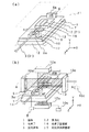
つぎに、本発明の光モジュールを図1(a)〜(b)を参照しながら説明する。本発明による光モジュールは、図1(a)にその一実施形態である光モジュールの説明図が示されるように、たとえば基板1上に光素子2と光伝送体固定台3aとが固着され、光素子2と光伝送体3とを結合させ光伝送体3が光伝送体固定台3aに固着されている。本発明では、基板1が、光素子固着部16と光伝送体固着部17との間に貫通孔13を有する基板からなっていることに特徴がある。
【0013】
基板1は、光素子固着部16と光伝送体固着部17との間に貫通孔13を有する絶縁性基板からなっている。なお、図1に示される例では、光素子2は、サブマウント7を介して、光伝送体3は光伝送体固定台3aを介して固着されている。また、基板1は、AlNやSiCなどの熱伝導率のよい基板からなることが放熱性の観点から好ましいが、これに限定されるものではなく、熱伝導率の劣るAl2O3、石英基板やガラスセラミックス基板などでもよい。また、基板の大きさは、たとえば、X方向は6mm程度、Y方向は1mm程度、Z方向は8mm程度の大きさからなっているが、この大きさに限定されない。ここにZ方向とは、光素子2と光伝送体3を結ぶ光軸方向をいい、Y方向とは、光素子2が固着された基板1の面と垂直方向をいい、X方向とは、Y方向およびZ方向と垂直方向をいう(図1参照)。
【0014】
貫通孔13は、光素子固着部16と光伝送体固着部17の間に基板1を貫通するように形成されている。このように形成されることにより、たとえば、光伝送体3を光伝送体固定台3aにハンダ付けにより固着する際、熱が光素子2に伝わるのに時間がかかり、光素子2の温度上昇を防ぐことができ、光素子の特性を劣化させない。また、このような観点からも、貫通孔13の大きさは、大きい方がハンダ付けの際の熱が光素子2側へさらに伝わりにくくなる点でも好ましいが、基板1の強度との関係で0.5mm程度の幅(W)で基板1の幅の50%程度の長さ(L)以下に形成される。そして、貫通孔13は、後述するように、X方向の位置合せの際、レーザマイクロメータ出射部10aから出射される平行光線を透過させることが好ましく、平行光線を透過させることができる幅(W)を有し、長さ(L)は、ビームの幅よりも小さくなるように形成することが位置合せの際、基板1の貫通孔13の端部を基準として、光伝送体3の位置を相対的に測定できる点で望ましい。
【0015】
光伝送体固定台3aは、ガラスセラミックス、ムライト(Al2O3とMgOを混合したもの)、石英など放熱の悪いものを用いることが望ましい。すなわち、後述するように、光ファイバ31などの光伝送体3を用いて光伝送体固定台3aにハンダ材5で固着する場合、ハンダ材5を溶融すると共に光伝送体3を固着するためにホットピンセットなどを用いて加熱することになるが、光伝送体固定台3aおよび基板1を介して、光素子2にも熱が伝わることになる。そのため、光素子2の特性が劣化する可能性があり、それを防ぐために光伝送体固定台3aに放熱の悪い材料を用いることで、ハンダ材5を溶融する際の熱が光素子2側へ伝わりにくくすることができる。
【0016】
光素子2は、半導体レーザや発光ダイオードなどの発光デバイス、フォトダイオードなどの受光デバイスの他、発光デバイスや受光デバイスと結合されるレンズまたはこれらの結合体や光導波路などの光伝送体と正確な位置合せをして組み立てるものをいい、たとえば、図1(a)に示される例では、光素子2として半導体レーザチップ21を用いており、EDFAの励起光源としては、980nm帯InGaAs系の高出力半導体レーザが用いられる。
【0017】
光素子2は、一般的にはAlNなどの熱伝導性のよいサブマウント7上に別途光素子2を図示しないハンダ材でダイボンディングされ、光素子2がダイボンディングされたサブマウント7が基板1上の予め決められた位置にAu−Sn合金などの図示しないハンダ材を用いて固着されており、この場合の光素子固着部16は、サブマウント7と基板1の間の基板1側の固着部となる。なお、基板1上にサブマウント7を先に固着しておき、その上に光素子2をダイボンディングすることも可能であり、サブマウント7を介することなく、直接光素子2が基板1上に固着されてもよく、この場合には光素子2と基板1との間の、基板1側の固着部となる。
【0018】
また、光素子2の他の例として、たとえば図2(a)に示されるように、半導体レーザチップ21とレンズ22とを一体的に結合した結合体であってもよい。結合体は、半導体レーザチップ21とレンズ22がサブマウント7上に形成されており、レンズ22は、半導体レーザチップ21から出射される光を集光し平行光線とし、光伝送体3、たとえば後述の光学部品組立体32へ伝送させるためのものである。具体的には、図2(a)に示されるようにサブマウント7上に、YAG溶接などによりレンズブラケット22aなどが形成され、その後、半導体レーザチップ21が固着されると共に、レンズブラケット22aにレンズ22が接着剤などで固着されることにより、形成される。なお、レンズが直接サブマウント7上に設けられていてもよい。さらに、光素子2がこれら以外のもの、たとえばキャンパッケージの半導体レーザ、光導波路、複数のレンズなどと半導体レーザチップ21などの発光デバイスを組み合せた結合体などでもよく、さらに、発光デバイスの代わりにフォトダイオードなどの受光デバイスでもよい。
【0019】
サブマウント7は、熱伝導性のよいものが光素子2の駆動時に光素子2から発せられる熱を基板1側へ放熱しやすいため好ましいが、これに限定されることはなく、たとえばシリコン基板上に酸化膜が形成されたサブマウントであってもよい。
【0020】
また、サブマウント7表面、または基板1上には受光素子6が設けられている。受光素子6は、サブマウント7に内蔵されていてもよいし、基板1上のいずれかの場所に受光素子固定台6aを介して個別に設けられていてもよい。すなわち、光素子2から出射される光の一部を受光できる位置に設置されていればよい。受光素子6は光素子2から出射される光を受けることで、光素子2の光出力をモニターし、光出力を一定に保つようにオートパワーコントロール駆動(以下、APC駆動という)を行うためのものであり、SiやInGaAsなどからなるフォトダイオードが一般に用いられる。
【0021】
光伝送体3は、光ファイバ31などの光伝送路の他、光伝送路と結合されるアイソレータや集光レンズなどからなる光学部品組立体32をいい、図1に示される例では、石英からなる光ファイバ31を用いており、光伝送体固定台3a上に載置され、かつ、その一端部が貫通孔13上を通過し、光素子2と後述する結合方法によって結合されるように固定されており、この場合の光伝送体固着部17は、光伝送体固定台3aと基板1との間の、基板1側の固着部をいう。また、光伝送体固定台3aを設けることなく、直接基板1に光伝送体3が固定されてもよく、この場合には、光伝送体3と基板1との間の、基板1側の固着部をいう。直接光ファイバ31を用いる場合、先端くさび形レンズドファイバを用いることが、さらに結合効率を上げられる点で望ましい。すなわち、先端くさび形レンズドファイバは、Y方向が球面レンズとなっており、たとえば光素子2として半導体レーザチップ21を用いている場合、一般的にY方向の光放射角が大きくなるが、このファイバを用いれば結合効率は落ちない。
【0022】
さらに、光伝送体3としてメッキ付きの光ファイバを用いる場合には、光ファイバ31を事前に加熱することが位置精度をあげるためにも望ましい。すなわち、たとえばNi/Auメッキされた光ファイバ31は、メッキによって応力がかかっており、熱を与えると光ファイバ31のY方向の位置が10μm程度変形することを本発明者らは見出し、一度光ファイバ31を熱することでメッキの応力が緩和され、再度熱してもほとんど変動しないことをさらに見出した。そのため、メッキ付きの光ファイバ31を用いる場合、たとえば150〜400℃で10〜60秒程度、好ましくは300℃で30秒程度の加熱処理を予め行うことが位置合せ時のずれ量をさらに減らすことができる点で望ましい。
【0023】
光伝送体3の他の例として、光ファイバに接続する光学部品組立体32であってもよい。たとえば、図2(b)に示されるように、光学部品組立体32は、コリメートレンズ32a、アイソレータ32b、集光レンズ32c、スリーブ32d、フェルール32eなどを筒32f内に組合せたものからなり、光素子2から出射される光を集光し、光学部品組立体32の一端部に結合される光ファイバ31などへ伝送させるためのものである。なお、光学部品組立体32は、上述の構成以外の構成でもよい。すなわち、半導体レーザチップ21から出射される光を伝送する構成となっており、レーザマイクロメータ10の光を透過または屈折させない構成となっているものであればよく、たとえば、BK7(ボロンシリケートクラウンガラス)や石英などからなるロッドレンズなどの単一のレンズのようなものでも、レーザマイクロメータ10の光を透過または屈折させない構成となっていればよい。
【0024】
ペルチェ素子12は、光素子2を駆動する際に発生する熱を吸収することにより基板1上の温度コントロールを行うものであり、一般的にはp形とn形の熱電素子を複数個、電気的に直列に配置され、その両側をセラミック基板で挟み込んだ構造からなり、基板1上のサーミスタ15でモニターされた温度に基づいて制御されるものである。また、サーミスタ15とは、熱に敏感な抵抗体であり、MoやCoを主体とする遷移金属酸化物を焼結した半導体の感熱素子であり、サーミスタ15で検出された温度をモニタしてペルチェ素子12にフィードバックすることにより基板1の温度を一定に制御するものである。
【0025】
つぎに、貫通孔13を有する基板1を用いた場合のX方向の位置合せ、および本発明の光モジュールの製法について図1(b)を参照しながら説明する。
【0026】
図1(b)に示されるように、半導体レーザチップ21などが組み立てられた基板1をたとえばペルチェ素子などの温度一定の作業台14上に載置し、光ファイバ31からなる光伝送体3の一端部を筐体11の側壁の貫通孔を通して半導体レーザチップ21と対向するようにXYZ方向に0.1μm以下の微調整が可能なXYZステージなどの駆動機構8により固定する。なお、作業台14にも、基板1の貫通孔13に対応する部分に貫通孔が設けられている。そして、半導体レーザチップ21を駆動すると共に、光ファイバ31を駆動機構8により移動させて、半導体レーザチップ21との結合が最適位置になるように位置調整をする。位置調整は、光ファイバ31を光伝送体固定台3a上に配設し、半導体レーザチップ21をAPC駆動する。一方、光ファイバ31の他端部側に図示しない光出力測定器を設置しておき、光ファイバ31内に光を入射させ、光ファイバ31より伝達される出力をモニターし、最適位置になるよう光ファイバ31のXY方向を駆動機構8により調整することにより行う。なお、Z方向は、位置ずれに対して鈍感であるため、駆動機構8を用いるまでもなく調整可能であるが、駆動機構8を用いて調整してもよい。
【0027】
そして、その最適位置に合せた状態でレーザマイクロメータ10(10a、10b、10c)を用いて、X方向の絶対位置を測定する。なお、Y方向についても同様にレーザマイクロメータ10(10d、10e、10c)を用いて測定することができる。レーザマイクロメータ10(10a〜10e)とは、高精度寸法管理を可能とする非接触の高精度レーザ測長センサであり、レーザ発振器から出射されたレーザビームを高速回転しているポリゴンミラーで反射させ、コリメータレンズにより平行光線とする出射部10a、10d、平行光線を集光レンズにより受光素子に集める受光部10b、10eおよび受光部での受けた光を寸法に変換し表示する処理制御部10cからなり、出射部10a、10dから出射された平行光線が測定物を高速で走査し、受光部10b、10eで受光し、測定物に遮られることによる光の明暗に応じて、それを処理制御部10cで寸法として表示するものであり、分解能は、0.02μm程度であり、測定精度は、0.1μm程度を有するものである。
【0028】
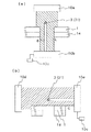
このレーザマイクロメータ10を用いることにより、ハンダ材5で固着後のずれ量の絶対値を検出することができ、補正の際に光素子2との相対位置を再度検出することなく、正確に位置合せをすることができる。たとえば、図1(b)に示されるように、X方向の測定では、貫通孔13に対向するようにY方向にレーザマイクロメータ10の出射部10aと受光部10bとを設置し、出射部10aから出射された平行光線が貫通孔13を透過し、受光部10bへ到達し、処理制御部10cでX方向の寸法に変換する。同様にY方向については、レーザマイクロメータ10(10d、10e、10c)をX方向に設置し、Y方向の寸法に変換する。さらにX方向の絶対位置の測定については、たとえば図3(a)に基板断面図(図1(b)のA−A方向断面図で、レーザマイクロメータ10a、10bを主体とした図)が示されるように、基板の貫通孔の幅(L)よりも幅の広い平行光線を出射部10aから出射し、受光部10bにおいては、基板1の影になる箇所、および光ファイバ31の影になる箇所は受光しないことになるため、貫通孔13の端を基準として、光ファイバ31の相対的位置(図3(a)の距離B)の測定が可能となる。なお、レーザマイクロメータ10のビーム幅の端部を基準とすることも可能であるが、レーザマイクロメータ10が少しでも動くと、測定値にくるいが生じるため、上述の貫通孔の端部を基準とした位置(B)を測定するのが好ましい。なお、Y方向についても、図3(b)の基板断面図(図1(b)のA−A方向断面図でレーザマイクロメータ10d、10eを主体とした図)に示されるように、基板1の表面を基準として距離Cを測定することができる。
【0029】
つぎに、位置調整された光ファイバ31を光伝送体固定台3aにハンダ材5により固着する。ハンダ材5による固着は、光ファイバ31の周りにハンダ材5をセットし、ホットピンセットなどを用いてたとえば300℃程度で加熱処理を行うことによってハンダ材5を溶融し、その後冷却することにより行う。なお、ハンダ材5は、図1(a)〜(b)に示される例では、Au−Sn合金(Au80at%含有)を用いているが、これらに限定されるものではなく、Au−Sn合金のAu含有率を変えたものやSn−Pb合金やInなども用いることができる。このようにハンダ材5を用いることにより、YAGレーザを用いた溶接による固着とは異なり、簡単に固着を解除でき、再度固着することができる。すなわち、YAGレーザを用いて固着してしまうと位置ずれが生じている場合の補正が難しく、また、精度も悪く、再調整にも限界があるのに対して、ハンダ材5を用いれば何度でも補正できる。
【0030】
つぎに、ハンダ材5によって固着した後、光ファイバ31のX方向の位置をレーザマイクロメータ10により測定して最適位置として記憶されている値とのずれ量Δdを検出する。そして、光ファイバ31の固着部を溶融して検出されたX方向のずれ量Δdだけ、駆動機構8により最適位置から光ファイバ31をずらせて再度固着する。再固着によっても、設定位置よりΔd近傍のずれが発生するため、予めΔdだけずらせて設定しておくことにより、最適位置付近で光ファイバ31が固着されることになる。この再固着後の光ファイバ31のX方向の位置を測定し、最適位置からのずれ量が大きい場合は、再度同じ調整を繰り返す。熱履歴の再現性がない(同じ温度を印加してもずれ量が異なる)場合に、調整後でもずれ量が発生する場合があるからである。なお、Y方向の位置合せについても同様に行う。そして、最後に光ファイバ31、半導体レーザチップ21を搭載した基板1を筐体11の中のペルチェ素子12上に組み込み、窒素雰囲気中で筐体11に蓋を閉め密封する。
【0031】
このように従来なら位置合せを行っても、実際には、位置合せ後に行う光ファイバなどの光伝送体を固着する時に位置ずれを生じてしまうため、それを補正する必要があり、YAGレーザによる溶接で光ファイバなどを固着する場合には、その複数回の補正が困難であり、一方、補正を可能とすべく、ハンダ材を用いて固着する場合にも、ハンダ材が溶融する際に、加熱処理などにより位置ずれしてしまい、光ファイバなどのずれの方向およびその絶対量が分からないため、完全な位置合せを行うことができないのに対して、本発明によれば、基板に貫通孔が設けられているため、光ファイバ31などの光伝送体3のX方向の位置調整にも、レーザマイクロメータを用いて、最初に最適な位置を決定し、ハンダ材で固着後、最適位置からのずれ量を検出することができる。すなわち、光伝送体と光素子との間に貫通孔を設けた基板を用いることにより、図1(b)に示されるようにレーザマイクロメータ出射部10aから出射された光は、光伝送体3の位置を認識しながら、貫通孔13を透過してレーザマイクロメータ受光部10bへ到達することになり、X方向の最適位置およびそのずれ量を正確に測定することができ、光素子と光伝送体との結合効率を高めることができる。
【0032】
さらに、この貫通孔が設けられることにより、ハンダ付けの際の熱は光素子側に伝達しづらく、動作時における光素子から発生する熱は基板直下に設けられるペルチェ素子などにより吸収されて温度上昇を防止することができる。
【0033】
前述の各例では、光素子2として半導体レーザチップ21、光伝送体3として光ファイバ31を用いた例であるが、これらに限定されることはなく、上述のその他の光素子や光伝送体を用いた場合でも同様に、熱による光素子の劣化を防ぎ、かつ、正確な位置合せを行うことができる。
【0034】
【発明の効果】
本発明によれば、基板が、光素子固着部と光伝送体固着部との間に貫通孔を有する基板からなることによって、ハンダ付けの際に発生する熱による光素子を劣化させることがなく、また組立の際にY方向のみならずX方向についても光素子と光伝送体との位置精度を少ない工数で正確に合せることができるため、非常に高特性で信頼性の高いが光モジュールを安価に得ることができる。
【図面の簡単な説明】
【図1】本発明による光モジュールの筐体内部、およびX方向ならびにY方向の位置合せを説明する斜視説明図である。
【図2】本発明による他の実施形態に係る光素子および光伝送体を説明する側面説明図である。
【図3】本発明による基板を用いた光伝送体の位置合せ方法を説明する断面説明図である。
【図4】従来の光モジュールの筐体内部の斜視説明図である。
【符号の説明】
1 基板
2 光素子
3 光伝送体
13 貫通孔
16 光素子固着部
17 光伝送体固着部[0001]
TECHNICAL FIELD OF THE INVENTION
The present invention relates to an optical module incorporating an optical element and an optical transmitter. More specifically, the present invention relates to an optical module in which a positional relationship between an optical element and an optical transmission body is adjusted with high accuracy and reliability is improved.
[0002]
[Prior art]
For example, an optical module incorporating a semiconductor laser chip and an optical fiber as an excitation light source is used in an EDFA (optical fiber amplifier) used as a relay point in a trunk line transmission line and playing a role of amplifying a signal. This type of optical module has a structure as shown in FIG. That is, the
[0003]
[Patent Document 1]
JP-A-7-333472 (FIG. 1)
[0004]
[Problems to be solved by the invention]
In the above-described optical module, since the optical fiber is fixed by soldering, there is an advantage that when a positional shift occurs, it can be corrected by melting the solder material again, but there is an advantage that the use of the solder material is disadvantageous. As a result, heat when the solder material is melted when the optical fiber is fixed is transmitted to the semiconductor laser chip, and there is a concern that the characteristics of the semiconductor laser chip may be deteriorated.
[0005]
In addition, as a method for precise alignment between an optical element such as a semiconductor laser chip and an optical transmission body such as an optical fiber, the present inventors use a laser micrometer to measure the absolute value of the amount of displacement at the time of fixing. And invented a method for simply and accurately aligning an optical element and an optical transmitter, which is disclosed in Japanese Patent Application No. 2002-320722. However, when the substrate is not a transmissive substrate, light is emitted from a laser micrometer. The reflected parallel light is reflected by the substrate, the light does not transmit to the light receiving unit, the amount of displacement in the direction parallel to the substrate (X direction) cannot be measured, and perfect alignment cannot be performed.
[0006]
The present invention has been made in view of such a situation, and the positional relationship between an optical element and an optical transmission body is accurately adjusted without deteriorating the optical element, the coupling efficiency is high, and an optical element or the like is used. An object is to provide an optical module with high reliability.
[0007]
[Means for Solving the Problems]
An optical module according to the present invention is an optical module in which an optical element is fixed on a substrate, the optical element is coupled to an optical transmitter, and the optical transmitter is fixed on the substrate. It consists of a substrate having a through hole between the element fixing portion and the optical transmission member fixing portion.
[0008]
Here, the optical element refers to a light emitting device such as a semiconductor laser or a light emitting diode, a light receiving device such as a photodiode, a lens coupled to the light emitting device or the light receiving device, or an optical transmission body such as a combination thereof or an optical waveguide. The term "optical transmission body" includes an optical transmission path such as an optical fiber, and an optical component assembly including an isolator and a condenser lens coupled to the optical transmission path. It is a meaning including.
[0009]
In addition, the term “fixed on the substrate” means not only a case where the substrate is fixed directly on the substrate but also a case where the substrate is fixed on the substrate via a fixing base or a submount. Further, the fixing portion refers to a fixing portion on the substrate side when directly fixing to the substrate, and when being fixed to the substrate via a submount or a fixing base, the submount or the fixing base and the substrate are fixed. Of the fixing surface on the substrate side.
[0010]
Thus, by providing the through hole between the optical element fixing portion of the substrate and the optical transmitter fixing portion, the heat generated at the time of soldering becomes difficult to be transmitted to the optical element side, and the heat generated by the optical element Deterioration can also be prevented. That is, since the heat generated at the time of soldering has the through holes, it takes time for the heat to reach the optical element without being transmitted to the optical element at the shortest distance, and it is difficult for the heat to be transmitted to the optical element. On the other hand, when the optical element generates heat by operation like a semiconductor laser chip, the heat is transmitted to the substrate immediately below via the submount, and is absorbed by the substrate kept at a constant temperature by a Peltier element or the like, and the heat of the optical element is removed. There is no fear that it will be higher than necessary.
[0011]
Further, even when the optical element and the optical transmitter are aligned using a light transmission type measuring device such as a laser micrometer, the light can be transmitted through the through hole, and the optical element can be transmitted. The positional relationship in the X direction (see FIG. 1) as well as the positional relationship in the X direction (see FIG. 1) between the optical transmitter and the optical transmission body are accurately matched, and the positional accuracy is improved. That is, the laser micrometer can be installed so as to face the through hole using a laser micrometer before the optical transmission body is fixed with the solder material, and the parallel light beam emitted from the laser micrometer emission part is transmitted through the through hole. Can be transmitted to the laser micrometer light receiving portion, and the optimum position in the X direction can also be measured. After fixing with the solder material, the position in the X direction is measured again using the laser micrometer, and the X direction is measured. Can be detected and corrected, the positional accuracy can be increased, and the coupling efficiency can be improved.
[0012]
BEST MODE FOR CARRYING OUT THE INVENTION
Next, an optical module according to the present invention will be described with reference to FIGS. In the optical module according to the present invention, for example, an
[0013]
The
[0014]
The through
[0015]
It is desirable that the optical transmission
[0016]
The
[0017]
The
[0018]
Further, as another example of the
[0019]
The submount 7 is preferably of a type having good thermal conductivity because heat generated from the
[0020]
The light receiving element 6 is provided on the surface of the submount 7 or on the
[0021]
The
[0022]
Further, when a plated optical fiber is used as the
[0023]
As another example of the
[0024]
The
[0025]
Next, the alignment in the X direction when the
[0026]
As shown in FIG. 1B, the
[0027]
Then, the absolute position in the X direction is measured using the laser micrometer 10 (10a, 10b, 10c) in a state where the position is adjusted to the optimum position. The measurement in the Y direction can be similarly performed using the laser micrometer 10 (10d, 10e, 10c). The laser micrometer 10 (10a to 10e) is a non-contact high-precision laser measuring sensor that enables high-precision dimensional control, and reflects a laser beam emitted from a laser oscillator by a polygon mirror rotating at high speed. The
[0028]
The use of the laser micrometer 10 makes it possible to detect the absolute value of the displacement amount after the
[0029]
Next, the
[0030]
Next, after fixing with the
[0031]
As described above, even if the positioning is conventionally performed, the positioning error actually occurs when the optical transmission medium such as the optical fiber is fixed after the positioning, and it is necessary to correct the positional deviation. When an optical fiber or the like is fixed by welding, it is difficult to make corrections a plurality of times.On the other hand, when fixing using a solder material to enable the correction, when the solder material is melted, According to the present invention, complete misalignment cannot be performed because the misalignment due to heat treatment or the like and the direction and absolute amount of misalignment of the optical fiber or the like are not known. In order to adjust the position of the
[0032]
Further, by providing the through holes, heat during soldering is difficult to be transmitted to the optical element side, and heat generated from the optical element during operation is absorbed by a Peltier element or the like provided immediately below the substrate to raise the temperature. Can be prevented.
[0033]
In each of the above-described examples, the
[0034]
【The invention's effect】
According to the present invention, since the substrate is formed of a substrate having a through hole between the optical element fixing portion and the optical transmitter fixing portion, the optical element does not deteriorate due to heat generated at the time of soldering. In addition, during assembly, not only in the Y direction but also in the X direction, the positional accuracy between the optical element and the optical transmission body can be accurately adjusted with a small number of man-hours. It can be obtained at low cost.
[Brief description of the drawings]
FIG. 1 is a perspective explanatory view illustrating the inside of a housing of an optical module according to the present invention, and alignment in an X direction and a Y direction.
FIG. 2 is an explanatory side view illustrating an optical element and an optical transmission body according to another embodiment of the present invention.
FIG. 3 is an explanatory cross-sectional view illustrating a method for aligning an optical transmitter using a substrate according to the present invention.
FIG. 4 is an explanatory perspective view of the inside of a housing of a conventional optical module.
[Explanation of symbols]
DESCRIPTION OF
Claims (1)
Priority Applications (2)
| Application Number | Priority Date | Filing Date | Title |
|---|---|---|---|
| JP2002350826A JP3947460B2 (en) | 2002-12-03 | 2002-12-03 | Optical module |
| US10/700,457 US7376312B2 (en) | 2002-11-05 | 2003-11-05 | Optical module and method for manufacturing the same |
Applications Claiming Priority (1)
| Application Number | Priority Date | Filing Date | Title |
|---|---|---|---|
| JP2002350826A JP3947460B2 (en) | 2002-12-03 | 2002-12-03 | Optical module |
Publications (2)
| Publication Number | Publication Date |
|---|---|
| JP2004184663A true JP2004184663A (en) | 2004-07-02 |
| JP3947460B2 JP3947460B2 (en) | 2007-07-18 |
Family
ID=32752909
Family Applications (1)
| Application Number | Title | Priority Date | Filing Date |
|---|---|---|---|
| JP2002350826A Expired - Fee Related JP3947460B2 (en) | 2002-11-05 | 2002-12-03 | Optical module |
Country Status (1)
| Country | Link |
|---|---|
| JP (1) | JP3947460B2 (en) |
Cited By (4)
| Publication number | Priority date | Publication date | Assignee | Title |
|---|---|---|---|---|
| JP2006108427A (en) * | 2004-10-06 | 2006-04-20 | Nec Engineering Ltd | Optical module assembling device and assembling method |
| JP2013541047A (en) * | 2010-10-07 | 2013-11-07 | アルカテル−ルーセント | Optoelectronic assembly for line card |
| US8787775B2 (en) | 2010-10-07 | 2014-07-22 | Alcatel Lucent | Opto-electronic assembly for a line card |
| JP6879440B1 (en) * | 2020-07-06 | 2021-06-02 | 三菱電機株式会社 | Optical receiver module |
-
2002
- 2002-12-03 JP JP2002350826A patent/JP3947460B2/en not_active Expired - Fee Related
Cited By (6)
| Publication number | Priority date | Publication date | Assignee | Title |
|---|---|---|---|---|
| JP2006108427A (en) * | 2004-10-06 | 2006-04-20 | Nec Engineering Ltd | Optical module assembling device and assembling method |
| JP2013541047A (en) * | 2010-10-07 | 2013-11-07 | アルカテル−ルーセント | Optoelectronic assembly for line card |
| US8787775B2 (en) | 2010-10-07 | 2014-07-22 | Alcatel Lucent | Opto-electronic assembly for a line card |
| JP6879440B1 (en) * | 2020-07-06 | 2021-06-02 | 三菱電機株式会社 | Optical receiver module |
| WO2022009259A1 (en) * | 2020-07-06 | 2022-01-13 | 三菱電機株式会社 | Light-receiving module |
| US11953375B2 (en) | 2020-07-06 | 2024-04-09 | Mitsubishi Electric Corporation | Light receiving module comprising stem and block on an upper surface of the stem |
Also Published As
| Publication number | Publication date |
|---|---|
| JP3947460B2 (en) | 2007-07-18 |
Similar Documents
| Publication | Publication Date | Title |
|---|---|---|
| JP3909257B2 (en) | Optical coupling device | |
| US7376312B2 (en) | Optical module and method for manufacturing the same | |
| US5857049A (en) | Precision alignment of optoelectronic devices | |
| US6659659B1 (en) | High-speed optical sub-assembly utilizing ceramic substrate, direct coupling and laser welding | |
| US5068865A (en) | Semiconductor laser module | |
| CN102043208B (en) | Cooled laser module | |
| GB2173917A (en) | Optical fibre connected to electro-optical transducer | |
| JP2004179273A (en) | Semiconductor laser chip component and semiconductor laser module using the same | |
| JP3518491B2 (en) | Optical coupling device | |
| US20050196112A1 (en) | Transmitting optical subassembly capable of monitoring the front beam of the semiconductor laser diode | |
| US20020018500A1 (en) | Semiconductor laser unit and semiconductor laser module | |
| JP2000277843A (en) | Semiconductor laser module and method of manufacturing the same | |
| US20210006036A1 (en) | Optical module | |
| JPS62276892A (en) | electronic components | |
| JP3947460B2 (en) | Optical module | |
| EP1353421B1 (en) | Optical module with a monitor photo diode | |
| JPH03120884A (en) | Semiconductor laser module | |
| JP2004079989A (en) | Optical module | |
| JP2004157208A (en) | Method for manufacturing optical module | |
| JP2013197256A (en) | Semiconductor laser module and manufacturing method therefor | |
| JP3925690B2 (en) | Semiconductor laser module | |
| US7293922B2 (en) | Non-mechanical adjustment of an optical fiber to an optical output port | |
| JP2005182014A (en) | Optimizing optical fiber alignment to optical output ports | |
| US7021835B1 (en) | Alignment of optical components in an optical subassembly | |
| JP3459286B2 (en) | Lens fixing device |
Legal Events
| Date | Code | Title | Description |
|---|---|---|---|
| A621 | Written request for application examination |
Free format text: JAPANESE INTERMEDIATE CODE: A621 Effective date: 20041228 |
|
| A977 | Report on retrieval |
Free format text: JAPANESE INTERMEDIATE CODE: A971007 Effective date: 20060731 |
|
| A131 | Notification of reasons for refusal |
Free format text: JAPANESE INTERMEDIATE CODE: A131 Effective date: 20060829 |
|
| A521 | Written amendment |
Free format text: JAPANESE INTERMEDIATE CODE: A523 Effective date: 20061030 |
|
| A131 | Notification of reasons for refusal |
Free format text: JAPANESE INTERMEDIATE CODE: A131 Effective date: 20061219 |
|
| A521 | Written amendment |
Free format text: JAPANESE INTERMEDIATE CODE: A523 Effective date: 20070208 |
|
| TRDD | Decision of grant or rejection written | ||
| A01 | Written decision to grant a patent or to grant a registration (utility model) |
Free format text: JAPANESE INTERMEDIATE CODE: A01 Effective date: 20070403 |
|
| A61 | First payment of annual fees (during grant procedure) |
Free format text: JAPANESE INTERMEDIATE CODE: A61 Effective date: 20070413 |
|
| R150 | Certificate of patent or registration of utility model |
Free format text: JAPANESE INTERMEDIATE CODE: R150 |
|
| LAPS | Cancellation because of no payment of annual fees |