JP2004200146A - Electroluminescence display device, method of manufacturing the same, and electronic apparatus - Google Patents
Electroluminescence display device, method of manufacturing the same, and electronic apparatus Download PDFInfo
- Publication number
- JP2004200146A JP2004200146A JP2003344803A JP2003344803A JP2004200146A JP 2004200146 A JP2004200146 A JP 2004200146A JP 2003344803 A JP2003344803 A JP 2003344803A JP 2003344803 A JP2003344803 A JP 2003344803A JP 2004200146 A JP2004200146 A JP 2004200146A
- Authority
- JP
- Japan
- Prior art keywords
- layer
- electrode
- substrate
- display device
- light emitting
- Prior art date
- Legal status (The legal status is an assumption and is not a legal conclusion. Google has not performed a legal analysis and makes no representation as to the accuracy of the status listed.)
- Pending
Links
Images


Classifications
-
- H—ELECTRICITY
- H05—ELECTRIC TECHNIQUES NOT OTHERWISE PROVIDED FOR
- H05B—ELECTRIC HEATING; ELECTRIC LIGHT SOURCES NOT OTHERWISE PROVIDED FOR; CIRCUIT ARRANGEMENTS FOR ELECTRIC LIGHT SOURCES, IN GENERAL
- H05B33/00—Electroluminescent light sources
- H05B33/12—Light sources with substantially two-dimensional [2D] radiating surfaces
- H05B33/26—Light sources with substantially two-dimensional [2D] radiating surfaces characterised by the composition or arrangement of the conductive material used as an electrode
-
- H—ELECTRICITY
- H10—SEMICONDUCTOR DEVICES; ELECTRIC SOLID-STATE DEVICES NOT OTHERWISE PROVIDED FOR
- H10K—ORGANIC ELECTRIC SOLID-STATE DEVICES
- H10K59/00—Integrated devices, or assemblies of multiple devices, comprising at least one organic light-emitting element covered by group H10K50/00
- H10K59/80—Constructional details
- H10K59/805—Electrodes
- H10K59/8052—Cathodes
- H10K59/80524—Transparent cathodes, e.g. comprising thin metal layers
-
- H—ELECTRICITY
- H10—SEMICONDUCTOR DEVICES; ELECTRIC SOLID-STATE DEVICES NOT OTHERWISE PROVIDED FOR
- H10K—ORGANIC ELECTRIC SOLID-STATE DEVICES
- H10K50/00—Organic light-emitting devices
- H10K50/80—Constructional details
- H10K50/805—Electrodes
- H10K50/82—Cathodes
- H10K50/828—Transparent cathodes, e.g. comprising thin metal layers
-
- H—ELECTRICITY
- H10—SEMICONDUCTOR DEVICES; ELECTRIC SOLID-STATE DEVICES NOT OTHERWISE PROVIDED FOR
- H10K—ORGANIC ELECTRIC SOLID-STATE DEVICES
- H10K2102/00—Constructional details relating to the organic devices covered by this subclass
- H10K2102/301—Details of OLEDs
- H10K2102/302—Details of OLEDs of OLED structures
- H10K2102/3023—Direction of light emission
- H10K2102/3026—Top emission
-
- H—ELECTRICITY
- H10—SEMICONDUCTOR DEVICES; ELECTRIC SOLID-STATE DEVICES NOT OTHERWISE PROVIDED FOR
- H10K—ORGANIC ELECTRIC SOLID-STATE DEVICES
- H10K59/00—Integrated devices, or assemblies of multiple devices, comprising at least one organic light-emitting element covered by group H10K50/00
- H10K59/10—OLED displays
- H10K59/12—Active-matrix OLED [AMOLED] displays
- H10K59/131—Interconnections, e.g. wiring lines or terminals
-
- H—ELECTRICITY
- H10—SEMICONDUCTOR DEVICES; ELECTRIC SOLID-STATE DEVICES NOT OTHERWISE PROVIDED FOR
- H10K—ORGANIC ELECTRIC SOLID-STATE DEVICES
- H10K85/00—Organic materials used in the body or electrodes of devices covered by this subclass
- H10K85/10—Organic polymers or oligomers
- H10K85/111—Organic polymers or oligomers comprising aromatic, heteroaromatic, or aryl chains, e.g. polyaniline, polyphenylene or polyphenylene vinylene
- H10K85/113—Heteroaromatic compounds comprising sulfur or selene, e.g. polythiophene
-
- H—ELECTRICITY
- H10—SEMICONDUCTOR DEVICES; ELECTRIC SOLID-STATE DEVICES NOT OTHERWISE PROVIDED FOR
- H10K—ORGANIC ELECTRIC SOLID-STATE DEVICES
- H10K85/00—Organic materials used in the body or electrodes of devices covered by this subclass
- H10K85/10—Organic polymers or oligomers
- H10K85/111—Organic polymers or oligomers comprising aromatic, heteroaromatic, or aryl chains, e.g. polyaniline, polyphenylene or polyphenylene vinylene
- H10K85/114—Poly-phenylenevinylene; Derivatives thereof
-
- H—ELECTRICITY
- H10—SEMICONDUCTOR DEVICES; ELECTRIC SOLID-STATE DEVICES NOT OTHERWISE PROVIDED FOR
- H10K—ORGANIC ELECTRIC SOLID-STATE DEVICES
- H10K85/00—Organic materials used in the body or electrodes of devices covered by this subclass
- H10K85/10—Organic polymers or oligomers
- H10K85/111—Organic polymers or oligomers comprising aromatic, heteroaromatic, or aryl chains, e.g. polyaniline, polyphenylene or polyphenylene vinylene
- H10K85/115—Polyfluorene; Derivatives thereof
-
- H—ELECTRICITY
- H10—SEMICONDUCTOR DEVICES; ELECTRIC SOLID-STATE DEVICES NOT OTHERWISE PROVIDED FOR
- H10K—ORGANIC ELECTRIC SOLID-STATE DEVICES
- H10K85/00—Organic materials used in the body or electrodes of devices covered by this subclass
- H10K85/10—Organic polymers or oligomers
- H10K85/151—Copolymers
-
- H—ELECTRICITY
- H10—SEMICONDUCTOR DEVICES; ELECTRIC SOLID-STATE DEVICES NOT OTHERWISE PROVIDED FOR
- H10K—ORGANIC ELECTRIC SOLID-STATE DEVICES
- H10K85/00—Organic materials used in the body or electrodes of devices covered by this subclass
- H10K85/60—Organic compounds having low molecular weight
- H10K85/631—Amine compounds having at least two aryl rest on at least one amine-nitrogen atom, e.g. triphenylamine
Landscapes
- Physics & Mathematics (AREA)
- Optics & Photonics (AREA)
- Electroluminescent Light Sources (AREA)
- Physical Vapour Deposition (AREA)
- Manufacturing Of Electric Cables (AREA)
Abstract
【課題】 本発明は、トップエミッション構造を有するエレクトロルミネッセンス表示装置の透明陰極電極技術に関し、金属酸化物を成膜する際に下地膜の酸化を防止できるようにした、トップエミッション型のエレクトロルミネッセンス表示装置及びその製造方法並びにこの表示装置を備えた電子機器を提供することを目的とする。
【解決手段】 基板2上に、第1の電極111と、発光層110bを含む機能層110と、金属酸化物からなる透明な第2の電極12とが下層側から順に積層する。この際、第2の電極12の酸素濃度を膜厚方向で変化させ、第2の電極12と機能層110との界面付近の酸素濃度が、第2の電極12における平均の酸素濃度よりも低くなるようにする。
【選択図】 図4
PROBLEM TO BE SOLVED: To provide a transparent cathode electrode technology for an electroluminescence display device having a top emission structure, and to prevent oxidation of a base film when forming a metal oxide, and to provide a top emission type electroluminescence display. It is an object of the present invention to provide a device, a method for manufacturing the same, and an electronic device including the display device.
SOLUTION: On a substrate 2, a first electrode 111, a functional layer 110 including a light emitting layer 110b, and a transparent second electrode 12 made of a metal oxide are sequentially stacked from the lower layer side. At this time, the oxygen concentration of the second electrode 12 is changed in the film thickness direction so that the oxygen concentration near the interface between the second electrode 12 and the functional layer 110 is lower than the average oxygen concentration in the second electrode 12. To be.
[Selection diagram] Fig. 4
Description
本発明は、エレクトロルミネッセンス表示装置及びその製造方法並びにこのエレクトロルミネッセンス表示装置を備えた電子機器に関する。 The present invention relates to an electroluminescence display device, a method of manufacturing the same, and an electronic apparatus including the electroluminescence display device.
従来より、携帯電話やPDA等の携帯機器やパーソナルコンピュータ等の表示手段として、エレクトロルミネッセンス(以下、単にELともいう)表示装置が開発されている。
EL表示装置は、EL層(発光層)を一対の電極間に挟持してなる発光素子を基板面内に複数備えて構成され、各発光素子を独立に駆動制御することで所望の表示を行っている。このEL表示装置は、発光層からの光の取り出し方向の違いにより、例えば素子基板側から光を取り出すボトムエミッション型と、封止部材側から光を取り出すトップエミッション型のものとに分類できるが、材料選択の自由度等の理由から、これまで主にボトムエミッション型の構造について研究されてきた。
2. Description of the Related Art Conventionally, an electroluminescence (hereinafter, also simply referred to as EL) display device has been developed as a display means for a portable device such as a mobile phone or a PDA or a personal computer.
An EL display device includes a plurality of light-emitting elements each having an EL layer (light-emitting layer) sandwiched between a pair of electrodes on a substrate surface, and performs desired display by independently driving and controlling each light-emitting element. ing. The EL display devices can be classified into, for example, a bottom emission type in which light is extracted from the element substrate side and a top emission type in which light is extracted from the sealing member side, depending on a difference in a direction in which light is extracted from the light emitting layer. For the reasons such as the degree of freedom of material selection, a bottom emission type structure has been mainly studied so far.
一方、表示装置の分野では、大型化,高精細化,高輝度化に対するニーズが高く、EL表示装置についても大型化を目指した研究開発が盛んに行なわれている。しかし、上述のボトムエミッション型のEL表示装置を大型化した場合、電極に信号を供給する配線を太くする必要があり、これにより画素の開口率が低下するという課題があった。また、このように開口率が低下した場合、画素の輝度を確保するために発光層に大きな電流を流す結果、製品寿命が短くなるという課題も生じる。このため、近年、画素の開口率が配線等の構造に影響されないトップエミッション型の構造が注目され、盛んに研究されている(特許文献1参照)。
このようなトップエミッション型のEL表示装置では、EL層を挟む一対の電極の内、封止部材側(観察者側)の電極を透明電極とする必要がある。このような透明電極には、一般にITOやSnO2等の金属酸化物が用いられている。この金属酸化物は、酸素濃度を一定としたキャリアガス雰囲気下において金属材料を基板に対してスパッタリングすることで形成される。
ところで、金属酸化物は、その酸素含有量によって光透過率が変化することが知られており、十分な透明性を得るためには、その酸素含有量を一定量以上確保する必要がある。
しかしながら、EL層或いはEL層上に設けられた電子注入層(又は正孔注入層)の上に金属酸化物をスパッタして形成する場合、キャリアガス中の活性な酸素によって下地のEL層等が酸化され、発光特性が劣化してしまうという課題があった。
In such a top emission type EL display device, the electrode on the sealing member side (observer side) among the pair of electrodes sandwiching the EL layer needs to be a transparent electrode. For such a transparent electrode, a metal oxide such as ITO or SnO2 is generally used. This metal oxide is formed by sputtering a metal material on a substrate in a carrier gas atmosphere with a constant oxygen concentration.
By the way, it is known that the light transmittance of a metal oxide changes depending on its oxygen content, and it is necessary to secure a certain amount or more of the oxygen content in order to obtain sufficient transparency.
However, when a metal oxide is formed by sputtering on an EL layer or an electron injection layer (or a hole injection layer) provided on the EL layer, the underlying EL layer or the like is activated by active oxygen in a carrier gas. There has been a problem that the phosphor is oxidized and the light emission characteristics are deteriorated.
本発明は、上述の課題に鑑み創案されたもので、金属酸化物を成膜する際に下地膜の酸化を防止できるようにした、トップエミッション型のエレクトロルミネッセンス表示装置及びその製造方法並びにこの表示装置を備えた電子機器を提供することを目的とする。 The present invention has been made in view of the above problems, and has been made in view of the above. A top emission type electroluminescent display device, a method of manufacturing the same, and a display therefor, capable of preventing oxidation of a base film when forming a metal oxide. It is an object to provide an electronic device provided with the device.
上記目的を達成するために、本発明のエレクトロルミネッセンス表示装置は、基板上に、第1の電極と、発光層を含む機能層と、金属酸化物からなる透明な第2の電極とが下層側から順に積層されてなり、上記第2の電極の酸素濃度は膜厚方向で変化しており、上記第2の電極と上記機能層との界面付近の酸素濃度は、上記第2の電極における平均の酸素濃度よりも低いことを特徴とする。 In order to achieve the above object, an electroluminescent display device according to the present invention includes, on a substrate, a first electrode, a functional layer including a light-emitting layer, and a transparent second electrode made of a metal oxide on a lower layer side. And the oxygen concentration of the second electrode changes in the film thickness direction, and the oxygen concentration near the interface between the second electrode and the functional layer is an average of the oxygen concentration in the second electrode. Characterized by a lower oxygen concentration.
すなわち、本構成では、第2の電極における平均の酸素濃度は、表示に必要とされる透明性を得るために所定濃度以上に設定されるが、膜厚方向で見ると、例えば下層側(機能層側)の酸素濃度が上層側の酸素濃度に比べて低くなるような濃度勾配が生じており、機能層との界面付近における酸素濃度は上記所定濃度よりも少なくなっている。このため、スパッタリングにより機能層との界面付近に上記金属酸化膜を堆積する際に、キャリアガス中の酸素分圧を従来よりも低く設定することができ、成膜中に下地となる機能層が酸化されることを極力防止できる。これにより、機能層の発光効率の低下を防止して明るい表示を実現することができる。特に、機能層との界面付近の酸素濃度は略ゼロとすることが望ましく、これにより、成膜時における機能層の酸化によるダメージを最小限に抑えることができる。 That is, in the present configuration, the average oxygen concentration in the second electrode is set to a predetermined concentration or more to obtain the transparency required for display. A concentration gradient occurs such that the oxygen concentration on the layer side is lower than the oxygen concentration on the upper layer side, and the oxygen concentration near the interface with the functional layer is lower than the above-mentioned predetermined concentration. For this reason, when depositing the metal oxide film near the interface with the functional layer by sputtering, the oxygen partial pressure in the carrier gas can be set lower than before, and the functional layer serving as a base during film formation can be reduced. Oxidation can be prevented as much as possible. This makes it possible to prevent a decrease in the luminous efficiency of the functional layer and realize a bright display. In particular, it is desirable that the oxygen concentration near the interface with the functional layer be substantially zero, so that damage due to oxidation of the functional layer during film formation can be minimized.
なお、機能層は、例えば、発光層と、この発光層に電子や正孔を輸送/注入するための電子輸送/注入層や正孔輸送/注入層等との積層体として構成される。また、発光層単体で機能層を構成してもよい。
また、界面付近とは、機能層との界面から5nm以内の膜厚の範囲をいう。
Note that the functional layer is configured as a laminate of, for example, a light emitting layer and an electron transporting / injecting layer or a hole transporting / injecting layer for transporting / injecting electrons and holes into the light emitting layer. Further, the functional layer may be constituted by the light emitting layer alone.
In addition, the vicinity of the interface means a range of a film thickness within 5 nm from the interface with the functional layer.
本発明のエレクトロルミネッセンス表示装置の製造方法は、基板上に第1の電極を形成する工程と、上記第1の電極上に発光層を含む機能層を形成する工程と、酸素を含むキャリアガス雰囲気下で上記機能層上に金属材料をスパッタリングし、上記機能層上に金属酸化物からなる透明な第2の電極を形成する工程とを備え、上記スパッタリングにおいて、上記機能層上に堆積される上記金属酸化物の堆積量が増大するに従って上記キャリアガスの酸素分圧を増大させることを特徴とする。 According to the method of manufacturing an electroluminescence display device of the present invention, a step of forming a first electrode on a substrate, a step of forming a functional layer including a light emitting layer on the first electrode, and a carrier gas atmosphere containing oxygen Sputtering a metal material on the functional layer below and forming a transparent second electrode made of a metal oxide on the functional layer, wherein in the sputtering, the transparent electrode is deposited on the functional layer. The oxygen partial pressure of the carrier gas is increased as the deposition amount of the metal oxide increases.
本製造方法では、スパッタリングにより機能層上に金属酸化膜を堆積する際に、成膜初期の段階における酸素分圧を従来のものよりも低く設定することができる。このため、キャリアガス中の活性な酸素により機能層が酸化されることを極力防止でき、発光効率の高い表示装置を得ることができる。また、金属酸化膜の堆積量が増加するに従って、キャリアガス中の酸素分圧を増大させているため、上層側の酸素濃度を高めて第2の電極全体としての酸素濃度を上記所定濃度以上とすることで、第2の電極全体として、表示に必要な透明性を得ることができる。 In the present manufacturing method, when depositing a metal oxide film on the functional layer by sputtering, the oxygen partial pressure in the initial stage of film formation can be set lower than that of the conventional method. Therefore, the functional layer can be prevented from being oxidized by active oxygen in the carrier gas as much as possible, and a display device with high luminous efficiency can be obtained. Further, as the deposition amount of the metal oxide film increases, the oxygen partial pressure in the carrier gas is increased. Therefore, the oxygen concentration in the upper layer is increased to make the oxygen concentration of the entire second electrode equal to or higher than the predetermined concentration. By doing so, transparency required for display can be obtained as the whole second electrode.
ここで、上記スパッタリングにおいて上記キャリアガスの酸素分圧を増大させるに際して、この酸素分圧を連続的又は段階的に増大させるようにするのが好ましい。このようにすることにより、表示に必要な透明性が得られる所望の平均酸素濃度が、容易に得られるようになる。
また、上記スパッタリングにおいて上記堆積量が所定の膜厚よりも少ない場合にキャリアガス中の酸素分圧を略ゼロとすることで、機能層の酸化を完全に防止することができる。
Here, when the oxygen partial pressure of the carrier gas is increased in the sputtering, the oxygen partial pressure is preferably increased continuously or stepwise. This makes it easy to obtain a desired average oxygen concentration at which the transparency required for display is obtained.
In addition, when the deposition amount is smaller than a predetermined film thickness in the sputtering, the oxygen partial pressure in the carrier gas is set to approximately zero, whereby the oxidation of the functional layer can be completely prevented.
また、上記所定の膜厚は、5nm以上、30nm以下であることが好ましい。例えば、成膜量が5nmよりも薄い状態で酸素の供給を開始した場合には、下地の機能層が酸化されて十分な発光効率が得られない。一方、金属材料のみを30nmよりも厚く成膜した場合には、第2の電極が黒ずみ、表示品質が著しく劣化する。 Further, the predetermined film thickness is preferably 5 nm or more and 30 nm or less. For example, when the supply of oxygen is started in a state where the film formation amount is thinner than 5 nm, the underlying functional layer is oxidized and sufficient luminous efficiency cannot be obtained. On the other hand, when only a metal material is formed to a thickness of more than 30 nm, the second electrode is darkened, and the display quality is significantly deteriorated.
また、本発明の電子機器は、上述のエレクトロルミネッセンス表示装置を備えたことを特徴とする。
本構成によれば、発光効率の高い表示部を備えた電子機器を提供することができる。
An electronic device according to another aspect of the invention includes the above-described electroluminescent display device.
According to this configuration, it is possible to provide an electronic device including a display portion with high luminous efficiency.
[第1実施形態]
以下、本発明の第1実施形態を図面を参照して説明する。なお、図1〜図18において、各層や各部材を図面上で認識可能な程度の大きさとするため、各層や各部材の縮尺は実際のものと異なるように表わしている。
[First Embodiment]
Hereinafter, a first embodiment of the present invention will be described with reference to the drawings. In FIGS. 1 to 18, the scale of each layer and each member is different from the actual scale in order to make each layer and each member have a size that can be recognized in the drawings.
図1は本実施形態のエレクトロルミネッセンス表示装置の一例である有機EL表示装置の配線構造を示す平面模式図である。
図1に示すように、本実施形態のエレクトロルミネッセンス表示装置1には、複数の走査線101と、走査線101に対して交差する方向に延びる複数の信号線102と、信号線102に並列に延びる複数の電源線103とがそれぞれ配線されている。そして、走査線101と信号線102とにより区画された領域が画素領域として構成されている。
FIG. 1 is a schematic plan view illustrating a wiring structure of an organic EL display device which is an example of the electroluminescent display device of the present embodiment.
As shown in FIG. 1, the
信号線102には、シフトレジスタ、レベルシフタ、ビデオライン及びアナログスイッチを備えるデータ側駆動回路104が接続されている。また、走査線101には、シフトレジスタ及びレベルシフタを備える走査側駆動回路105が接続されている。
The data
各画素領域には、走査線101を介して走査信号がゲート電極に供給されるスイッチング用の薄膜トランジスタ112と、このスイッチング用の薄膜トランジスタ112を介して信号線102から共有される画素信号を保持する保持容量capと、該保持容量capによって保持された画素信号がゲート電極に供給される駆動用の薄膜トランジスタ123と、この駆動用薄膜トランジスタ123を介して電源線103に電気的に接続したときに当該電源線103から駆動電流が流れ込む画素電極111と、この画素電極111と陰極12との間に挟み込まれる機能層110とが設けられている。画素電極111と対向電極12と機能層110により発光部Aが構成され、表示装置1は、この発光部Aをマトリクス状に複数備えて構成されている。
In each pixel region, a switching
係る構成によれば、走査線101が駆動されてスイッチング用の薄膜トランジスタ112がオンになると、そのときの信号線102の電位が保持容量capに保持され、該保持容量capの状態に応じて、駆動用の薄膜トランジスタ123のオン・オフ状態が決まる。そして、駆動用の薄膜トランジスタ123のチャネルを介して、電源線103から画素電極111に電流が流れ、更に機能層110を介して陰極12に電流が流れる。機能層110は、これを流れる電流量に応じて発光する。
According to such a configuration, when the
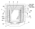
図2は本表示装置の平面模式図であり、図3は図2をI−I′断面で切った断面模式図である。
図3に示すように、本実施形態の表示装置1は、基板2上に回路素子部14と表示素子部10が順に積層され、この積層体の形成された基板面が封止部3によって封止された構造を有する。表示素子部10は、発光層110bを含む発光素子部11と、発光素子部11上に形成された陰極12とからなる。この陰極12及び封止部3は透光性を有しており、本表示装置1は、発光層から発した表示光が封止部3側から出射される、所謂トップエミッション型の表示装置として構成されている。
FIG. 2 is a schematic plan view of the present display device, and FIG. 3 is a schematic cross-sectional view of FIG. 2 taken along the line II ′.
As shown in FIG. 3, in the
基板2には、透明基板(又は半透明基板)又は不透明基板のいずれを用いることもできる。透明又は半透明な基板としては、例えばガラス、石英、樹脂(プラスチック、プラスチックフィルム)等が挙げられ、特に、安価なソーダガラス基板が好適に用いられる。不透明な基板としては、例えばアルミナ等のセラミックやステンレススチール等の金属シートに表面酸化等の絶縁処理を施したものの他に、熱硬化性樹脂、熱可塑性樹脂等が挙げられる。また、基板2は、図2に示すように、中央に位置する表示領域2aと、基板2の周縁に位置して表示領域2aを囲む非表示領域2bとに区画されている。
表示領域2aは、マトリックス状に配置された発光部Aによって形成される領域であり、表示領域の外側に非表示領域2bが形成されている。そして,非表示領域2bには、表示領域2aに隣接するダミー表示領域2dが形成されている。
As the
The
図3に示すように、回路素子部14には、前述の走査線、信号線、保持容量、スイッチング用の薄膜トランジスタ、駆動用の薄膜トランジスタ123等が備えられており、表示領域2aに配置された各発光部Aを駆動するようになっている。
陰極12は、その一端が発光素子部11上から基板2上に形成された陰極用配線120に接続しており、この配線の一端部がフレキシブル基板5上の配線5aに接続されている。また、配線5aは、フレキシブル基板5上に備えられた駆動IC6(駆動回路)に接続されている(図2参照)。
As shown in FIG. 3, the
One end of the
また、回路素子部14の非表示領域2bには、前述の電源線103(103R、103G、103B)が配線されている。
また、表示領域2aの図2中両側には、前述の走査側駆動回路105、105が配置されている。この走査側駆動回路105、105はダミー領域2dの下側の回路素子部14内に設けられている。更に回路素子部14内には、走査側駆動回路105、105に接続される駆動回路用制御信号配線105aと駆動回路用電源配線105bとが設けられている。
更に表示領域2aの図2中上側には検査回路106が配置されている。この検査回路106により、製造途中や出荷時の表示装置の品質、欠陥の検査を行うことができる。
The above-described power supply lines 103 (103R, 103G, 103B) are wired in the
The above-described scanning-
Further, an
封止部3は、基板2に塗布された封止樹脂603と、封止缶(封止部材)604とから構成されている。
封止樹脂603は、基板2と封止缶604を接着する接着剤であり、例えばマイクロディスペンサ等により基板2の周囲に環状に塗布されている。この封止樹脂603は、熱硬化樹脂あるいは紫外線硬化樹脂等からなり、特に、熱硬化樹脂の1種であるエポキシ樹脂よりなることが好ましい。また、この封止樹脂603には酸素や水分を通しにくい材料が用いられており、基板2と封止缶604の間から封止缶604内部への水又は酸素の侵入を防いで、陰極12または発光素子部11内に形成された発光層110bの酸化を防止するようになっている。
The
The sealing
ガラスや樹脂等の透光性部材からなる封止缶604は、その内側に表示素子10を収納する凹部604aが設けられており、封止樹脂603を介して基板2に接合されている。なお、封止缶604の内面側には、必要に応じて、非表示領域2bに対応する領域に、酸素や水分を吸収又は除去するゲッター材を設けることができる。このゲッター材としては、例えば、Li,Na,Rb,Cs等のアルカリ金属、Be,Mg,Ca,Sr,Ba等のアルカリ土類金属、アルカリ土類金属の酸化物、アルカリ金属又はアルカリ土類金属の水酸化物等を好適に用いることができる。アルカリ土類金属の酸化物は、水と反応して水酸化物に変化することにより、脱水材として作用する。アルカリ金属や、アルカリ土類金属は、酸素と反応して水酸化物に変化するとともに水と反応して酸化物に変化するため、
脱水材としてだけでなく脱酸素材としても作用する。これにより、発光部Aの酸化を防止でき、装置の信頼性を高めることができる。
The sealing can 604 made of a light-transmitting member such as glass or resin has a
It acts not only as a dehydrating material but also as a deoxidizing material. Thereby, the oxidation of the light emitting portion A can be prevented, and the reliability of the device can be improved.
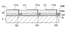
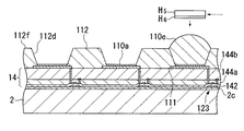
図4に、本表示装置における表示領域2aの断面構造を拡大した図を示す。この表示装置1は、基板2上に、TFTなどの回路等が形成された回路素子部14と、画素電極111と、発光層110bを含む機能層110が形成された発光素子部11と、陰極12とが順次積層されて構成されている。
FIG. 4 shows an enlarged view of the cross-sectional structure of the
回路素子部14には、基板2上にシリコン酸化膜からなる下地保護膜2cが形成され、この下地保護膜2c上に多結晶シリコンからなる島状の半導体膜141が形成されている。尚、半導体膜141には、ソース領域141a及びドレイン領域141bが高濃度Pイオン打ち込みにより形成されている。また、Pが導入されなかった部分がチャネル領域141cとなっている。
In the
また、回路素子部14には、下地保護膜2c及び半導体膜141を覆うゲート絶縁膜142が形成されている。そして、このゲート絶縁膜142上には、半導体膜141のチャネル領域141cに対応する位置に、Al、Mo、Ta、Ti、W等からなるゲート電極143(走査線101)が形成されている。そして、半導体膜141,ゲート絶縁膜142,ゲート電極143により薄膜トランジスタ123が構成されている。この薄膜トランジスタ123では、半導体膜141にポリシリコンを用いているため、高輝度,高精細な表示を実現できる。
In the
また、ゲート電極143及びゲート絶縁膜142上には透明な第1層間絶縁膜144aと第2層間絶縁膜144bが形成されており、この第1、第2層間絶縁膜144a,144bには、絶縁膜144a,144bを貫通して半導体膜141のソース、ドレイン領域141a,141bにそれぞれ接続されるコンタクトホール145,146が形成されている。コンタクトホール145は画素電極に接続されており、このコンタクトホール145を介して画素電極111と半導体のソース領域141aが電気的に接続されている。また、コンタクトホール146は電源線103に接続されており、このコンタクトホール146を介して、電源線103から画素信号が供給されるようになっている。
以上により駆動用の回路が構成されている。尚、回路素子部14には、前述した保持容量cap及びスイッチング用の薄膜トランジスタ142も形成されているが、図4ではこれらの図示を省略している。
Further, a transparent first
Thus, a driving circuit is configured. Note that the above-described storage capacitor cap and the switching
画素電極111は、第2層間絶縁膜144b上に平面視略矩形にパターニングされて形成されており、表示領域2a内にマトリクス状に複数配置されている。
この画素電極111には、例えばアルミニウム(Al)膜や銀(Ag)膜等の高反射率の金属膜が用いられており、基板2側に発した光を封止部3側に効率的に出射させるようになっている。
The
For the
発光素子部11は、複数の画素電極111上の各々に積層された機能層110と、各画素電極111及び機能層110の間に備えられて各機能層110を仕切るバンク層112とを主体として構成されている。機能層110上には陰極12が配置されており、これら画素電極111、機能層110及び陰極12によって発光部Aが構成されている。
The light emitting
バンク層112は、アクリル樹脂、ポリイミド樹脂等の耐熱性、耐溶媒性に優れたレジストからなり、画素電極111の形成位置に対応して開口部112dが形成されている。このバンク層112の厚さは、例えば0.1〜3.5μmの範囲が好ましく、特に2μm程度がよい。厚さが0.1μm未満では、後述する正孔注入/輸送層及び発光層の合計厚よりバンク層112が薄くなり、発光層が開口部112dから溢れるおそれがあるので好ましくない。また、厚さが3.5μmを越えると、開口部112dによる段差が大きくなり、バンク層112上に形成する陰極12のステップカバレッジを確保できなくなるので好ましくない。また、バンク層112の厚さを2μm以上にすれば、駆動用の薄膜トランジスタ123との絶縁を高めることができる点でより好ましい。
The
なお、バンク層112に仕切られた各領域において、画素電極111の電極面111aは酸素を処理ガスとするプラズマ処理によって親液処理されており、親液性を示す。一方、開口部112dの壁面及びバンク層112の上面112fは、4フッ化メタンを処理ガスとするプラズマ処理によって表面がフッ化処理(撥液処理)されており、撥液性を示す。
In each region partitioned by the
機能層110は、画素電極111上に積層された正孔注入/輸送層110aと、正孔注入/輸送層110a上に隣接して形成された発光層110bと、この発光層110b上に隣接して形成された電子注入層110cとから構成されている。
正孔注入/輸送層110aは、正孔を発光層110bに注入する機能を有するとともに、正孔を正孔注入/輸送層110a内部において輸送する機能を有する。この正孔注入/輸送層形成材料としては、例えば、ポリエチレンジオキシチオフェン等のポリチオフェン誘導体とポリスチレンスルホン酸等の混合物を用いることができる。また、電子注入層110cは、電子を発光層110bに注入する機能を有するとともに、電子を電子注入層110c内部において輸送する機能を有する。この電子注入層110cとしては、例えばリチウムキノリノール(Liq)やフッ化リチウム(LiF)或いはバソフェンセシウム等を好適に用いることができる。また、仕事関数が4eV以下の金属、例えばMg、Ca、Ba、Sr、Li、Na、Rb、Cs、Yb、Smなども用いることができる。
The
The hole injection /
このような正孔注入/輸送層110a,電子注入層110cを、それぞれ画素電極111と発光層110bの間、及び、陰極12と発光層110bとの間に設けることにより、発光層110bの発光効率、寿命等の素子特性が向上する。なお、正孔注入/輸送材料は、各色の発光層110b毎に異ならせてもよく、又、特定の色の発光層110bに対して正孔注入/輸送層110aを設けない構成とすることも可能である。
By providing such a hole injection /
発光層110bは、赤色(R)に発光する赤色発光層110b1、緑色(G)に発光する緑色発光層110b2、及び青色(B)に発光する青色発光層110b3、の3種類を有し、各発光層110b1〜110b3がストライプ配置されている。この発光層110bの材料としては、例えば、[化1]〜[化5]に示す(ポリ)パラフェニレンビニレン誘導体、ポリフェニレン誘導体、ポリフルオレン誘導体、ポリビニルカルバゾール、ポリチオフェン誘導体、ペリレン係色素、クマリン系色素、ローダミン系色素、またはこれらの高分子材料にルブレン、ペリレン、9,10-ジフェニルアントラセン、テトラフェニルブタジエン、ナイルレッド、クマリン6、キナクリドン等をドープして用いることができる。
The

陰極12には、例えばインジウム錫酸化物(ITO)やインジウム亜鉛酸化物(IZO)等の金属酸化物からなる透光性の導電材料が用いられており、陰極12は発光素子部11の全面に形成されている。そして、画素電極111と対になって機能層110に電流を流す役割を果たす。この陰極12の酸素含有量は膜厚方向に変化しており、下層側が上層側に比べて酸素含有量が少なくなっている。すなわち、陰極12の平均酸素濃度は、表示に必要とされる透明性を得るために所定濃度以上に設定されるが、膜厚方向で見ると、下層側(機能層110側)の酸素濃度が上層側(封止部3側)の酸素濃度に比べて小さくなるように、濃度勾配が生じている。
For the
例えば、陰極12は、図4に示すように、酸素濃度が略ゼロである無酸素層12aと、酸素濃度が平均酸素濃度よりも大きい有酸素層12bとが下層側から順に積層された構造を有している。このような陰極12は、キャリアガス(例えばAr)中の酸素分圧を経時的に変化させながら、インジウム(In)や錫(Sn)等の金属材料を機能層110上にスパッタすることで形成される。
For example, as shown in FIG. 4, the
具体的には、成膜開始直後の一定時間内(即ち、機能層110上の金属酸化物の堆積量が所定の膜厚よりも少ない場合)では、キャリアガス中の酸素分圧を略ゼロとし、その後、酸素分圧を連続的又は段階的に増加させることで、所望の平均酸素濃度が容易に得られるようにしている。このように成膜開始直後の酸素分圧を略ゼロとすることで、キャリアガス中の活性な酸素によって機能層110が酸化されることを防止することができる。なお、酸素分圧を略ゼロとして形成する金属材料の膜厚は、例えば5nm以上30nm以下の範囲であることが好ましい。成膜量が5nmよりも薄い状態で酸素の供給を開始すると、成膜された金属材料の結晶粒界を通して酸素が機能層110内に侵入し、機能層110が酸化されてしまう。一方、金属材料の膜厚が30nmよりも厚くなると、陰極12が黒ずみ、表示品質が著しく劣化する。
Specifically, within a certain period of time immediately after the start of film formation (that is, when the amount of metal oxide deposited on the
なお、陰極12上には必要に応じてSiO,SiO2,SiN等からなる酸化防止用の保護層を設けても良い。
Note that a protective layer made of SiO, SiO 2 , SiN or the like for preventing oxidation may be provided on the
次に、本実施形態の表示装置の製造方法を図面を参照して説明する。
本実施形態の表示装置1の製造方法は、例えば、(1)バンク部形成工程、(2)プラズマ処理工程(3)正孔注入/輸送層形成工程(第1液滴吐出工程を含む)、(4)発光層形成工程(第2液滴吐出工程を含む)、(5)電子注入層形成工程、(6)陰極形成工程、及び(7)封止工程とを具備して構成されている。なお、製造方法はこれに限られるものではなく必要に応じてその他の工程が除かれる場合、また追加される場合もある。
Next, a method for manufacturing the display device of the present embodiment will be described with reference to the drawings.
The method for manufacturing the
(1)バンク層形成工程
バンク層形成工程は、基板2の所定の位置に開口部112dを有するバンク層112を形成する工程である。以下に形成方法について説明する。
まず、図5に示すように、基板2上に走査線,信号線,薄膜トランジスタ123等の回路素子部14を有し、層間絶縁膜144a,144bの上に複数の画素電極111が形成された素子基板を準備する。
そして、この基板2上にアクリル樹脂、ポリイミド樹脂等の耐熱性、耐溶剤性を有する感光性材料を塗布し、フォトリソグラフィ技術により、画素電極111の配置された領域に開口部112dを形成する(図6参照)。なお、バンク層112の厚さは、0.1〜3.5μmの範囲が好ましく、特に2μm程度がよい。このような範囲とする理由は以下の通りである。
(1) Bank Layer Forming Step The bank layer forming step is a step of forming a
First, as shown in FIG. 5, an element having a
Then, a heat-resistant and solvent-resistant photosensitive material such as an acrylic resin or a polyimide resin is applied on the
すなわち、厚さが0.1μm未満では、後述する正孔注入/輸送層及び発光層の合計厚よりバンク層112が薄くなり、発光層110bが開口部112dから溢れてしまうおそれがあるので好ましくない。また、厚さが3.5μmを越えると、開口部112dによる段差が大きくなり、開口部112dにおける陰極12のステップカバレッジが確保できなくなるので好ましくない。また、バンク層112の厚さを2μm以上にすれば、陰極12と駆動用の薄膜トランジスタ123との絶縁を高めることができる点で好ましい。
That is, if the thickness is less than 0.1 μm, the
(2)プラズマ処理工程
プラズマ処理工程は、画素電極111の表面を活性化すること、更にバンク層112の表面を表面処理する事を目的として行われる。特に活性化工程では、画素電極111上の洗浄、更に仕事関数の調整を主な目的として行っている。更に、画素電極111の表面の親液化処理、バンク層112表面の撥液化処理を行う。
このプラズマ処理工程は、例えば(2)−1予備加熱工程、(2)−2活性化処理工程(親液性にする親液化工程)、(2)−3撥液化処理工程、及び(2)−4冷却工程に大別される。なお、このような工程に限られるものではなく、必要に応じて工程を削減、更なる工程追加も行われる。
(2) Plasma Treatment Step The plasma treatment step is performed for the purpose of activating the surface of the
This plasma processing step includes, for example, (2) -1 preheating step, (2) -2 activation processing step (a lyophilic step for making lyophilic), (2) -3 lyophobic processing step, and (2) -4 cooling process. It is to be noted that the present invention is not limited to such steps, and steps may be reduced and further steps may be added as necessary.
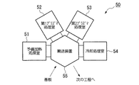
図7に、プラズマ処理工程で用いられるプラズマ処理装置を示す。
図7に示すプラズマ処理装置50は、予備加熱処理室51、第1プラズマ処理室52、第2プラズマ処理室53、冷却処理室54、これらの各処理室51〜54に基板2を搬送する搬送装置55とから構成されている。各処理室51〜54は、搬送装置55を中心として放射状に配置されている。
FIG. 7 shows a plasma processing apparatus used in the plasma processing step.
The
まず、これらの装置を用いた概略の工程を説明する。
予備加熱工程は予備加熱処理室51において行われ、バンク層形成工程から搬送された基板2を所定の温度に加熱する。
予備加熱工程の後、親液化工程及び撥液化処理工程を行う。すなわち、基板2を第1,第2プラズマ処理室52,53に順次搬送し、それぞれの処理室52,53においてバンク層112にプラズマ処理を行い親液化する。この親液化処理後に撥液化処理を行う。撥液化処理の後に基板2を冷却処理室に搬送し、冷却処理室54おいて基板2を室温まで冷却する。この冷却工程後、搬送装置55により次の工程である正孔注入/輸送層形成工程に基板2を搬送する。
First, a schematic process using these devices will be described.
The preheating step is performed in the preheating
After the preheating step, a lyophilic step and a lyophobic treatment step are performed. That is, the
以下に、それぞれの工程について詳細に説明する。
(2)−1 予備加熱工程
予備加熱工程は予備加熱処理室51により行う。この処理室51において、バンク層112を含む基板2を所定の温度まで加熱する。
基板2の加熱方法は、例えば処理室51内にて基板2を載せるステージにヒータを取り付け、このヒータで当該ステージごとに基板2を加熱する手段がとられている。なお、これ以外の方法を採用することも可能である。
この予備加熱処理室51では、基板2は例えば70℃〜80℃の範囲で加熱される。この温度は次工程であるプラズマ処理における処理温度であり、次の工程に合わせて基板2を事前に加熱し、基板2の温度ばらつきを解消することを目的としている。
Hereinafter, each step will be described in detail.
(2) -1 Preheating Step The preheating step is performed in the preheating
As a method of heating the
In the preheating
仮に予備加熱工程を加えなければ、基板2は室温から上記のような温度に加熱されることになり、工程開始から工程終了までのプラズマ処理工程中において温度が常に変動しながら処理される事になる。したがって、基板温度が変化しながらプラズマ処理を行うことは、特性の不均一につながる可能性がある。したがって、処理条件を一定に保ち、均一な特性を得るために予備加熱を行うのである。
このため、プラズマ処理工程においては、第1,第2プラズマ処理装置52,53内の試料ステージ上に基板2を載置した状態で親液化工程または撥液化工程を行う場合に、予備加熱温度を、親液化工程または撥液化工程を連続して行う試料ステージ56の温度にほぼ一致させることが好ましい。
If the preheating step is not added, the
For this reason, in the plasma processing step, when performing the lyophilic step or the lyophobic step while the
すなわち、第1,第2プラズマ処理装置52,53内の試料ステージが上昇する温度、例えば70〜80℃まで予め基板2を予備加熱することにより、多数の基板にプラズマ処理を連続的に行った場合でも、処理開始直後と処理終了直前でのプラズマ処理条件をほぼ一定にすることができる。これにより、基板2間の表面処理条件を同一にし、バンク層112の組成物に対する濡れ性を均一化することができ、一定の品質を有する表示装置を製造することができる。
また、基板2を予め予備加熱しておくことにより、後のプラズマ処理における処理時間を短縮することができる。
That is, the plasma processing was continuously performed on a large number of substrates by preheating the
Further, by preheating the
(2)−2 活性化処理
第1プラズマ処理室52では、活性化処理が行われる。活性化処理には、画素電極111における仕事関数の調整、制御、画素電極表面の洗浄、画素電極表面の親液化処理が含まれる。
親液化処理として、大気雰囲気中で酸素を処理ガスとするプラズマ処理(O2プラズマ処理)を行う。図8は第1プラズマ処理を模式的に示した図である。図8に示すように、バンク層112を含む基板2は加熱ヒータ内臓の試料ステージ56上に載置され、基板2の上側にはギャップ間隔0.5〜2mm程度の距離をおいてプラズマ放電電極57が基板2に対向して配置されている。基板2は、試料ステージ56によって加熱されつつ、試料ステージ56は図示矢印方向に向けて所定の搬送速度で搬送され、その間に基板2に対してプラズマ状態の酸素が照射される。
(2) -2 Activation Process In the first
As the lyophilic process, a plasma process (O 2 plasma process) using oxygen as a process gas in an air atmosphere is performed. FIG. 8 is a diagram schematically showing the first plasma processing. As shown in FIG. 8, the
O2プラズマ処理の条件は、例えば、プラズマパワー100〜800kW、酸素ガス流量50〜100ml/min、板搬送速度0.5〜10mm/sec、基板温度70〜90℃の条件で行われる。なお、試料ステージ56による加熱は、主として予備加熱された基板2の保温のために行われる。
このO2プラズマ処理により、図9に示すように、画素電極111の電極面111a、及びバンク層112の開口部112dの壁面ならびに上面112fが親液処理される。この親液処理により、これらの各面に水酸基が導入されて親液性が付与される。
図9では、親液処理された部分を一点鎖線で示している。
なお、このO2プラズマ処理は、親液性を付与するのみならず、上述の通り画素電極111上の洗浄,仕事関数の調整も兼ねている。
The conditions for the O 2 plasma treatment are, for example, a plasma power of 100 to 800 kW, an oxygen gas flow rate of 50 to 100 ml / min, a plate transfer speed of 0.5 to 10 mm / sec, and a substrate temperature of 70 to 90 ° C. The heating by the
As shown in FIG. 9, the O 2 plasma treatment performs the lyophilic treatment on the
In FIG. 9, the portion subjected to the lyophilic treatment is indicated by a dashed line.
The O2 plasma treatment not only imparts the lyophilic property but also cleans the
(2)−3 撥液処理工程
第2プラズマ処理室53では、撥液化工程として、大気雰囲気中でテトラフルオロメタン(四フッ化炭素)等のフッ化物含有ガスを処理ガスとするプラズマ処理(CF4プラズマ処理)を行う。第2プラズマ処理室53の内部構造は図8に示した第1プラズマ処理室52の内部構造と同じである。即ち、基板2は、試料ステージによって加熱されつつ、試料ステージごと所定の搬送速度で搬送され、その間に基板2に対してプラズマ状態の処理ガスが照射される。
(2) -3 Liquid Repellent Treatment Step In the second
CF4プラズマ処理の条件は、例えば、プラズマパワー100〜800kW、4フッ化メタンガス流量50〜100ml/min、基板搬送速度0.5〜10mm/sec、基板温度70〜90℃の条件で行われる。なお、加熱ステージによる加熱は、第1プラズマ処理室52の場合と同様に、主として予備加熱された基板2の保温のために行われる。
なお、処理ガスは、テトラフルオロメタン(四フッ化炭素)に限らず、他のフルオロカーボン系のガスを用いることができる。
The conditions of the CF 4 plasma treatment are, for example, a plasma power of 100 to 800 kW, a flow rate of tetrafluoromethane gas of 50 to 100 ml / min, a substrate transfer speed of 0.5 to 10 mm / sec, and a substrate temperature of 70 to 90 ° C. The heating by the heating stage is performed mainly for keeping the
Note that the processing gas is not limited to tetrafluoromethane (carbon tetrafluoride), and other fluorocarbon-based gases can be used.
CF4プラズマ処理により、図10に示すように、開口部112d壁面及びバンク層112の上面112fが撥液処理される。この撥液処理により、これらの各面にフッ素基が導入されて撥液性が付与される。図10では、撥液性を示す領域を二点鎖線で示している。
尚、画素電極111の電極面111aもこのCF4プラズマ処理の影響を多少受けるが、濡れ性に影響を与える事は少ない。図10では、親液性を示す領域を一点鎖線で示している。
As shown in FIG. 10, the liquid repellency treatment is performed on the wall surface of the
Note that the
(2)−4 冷却工程
冷却工程として、冷却処理室54を用い、プラズマ処理のために加熱された基板2を管理温度まで冷却する。これは、この以降の工程であるインクジェット工程(液滴吐出工程)の管理温度まで冷却するために行う工程である。
この冷却処理室54は、基板2を配置するためのプレートを有し、そのプレートは基板2を冷却するように水冷装置が内蔵された構造となっている。
(2) -4 Cooling Step In the cooling step, the
The cooling processing chamber 54 has a plate on which the
このようにプラズマ処理後の基板2を室温、または所定の温度(例えばインクジェット工程を行う管理温度)まで冷却することにより、次の正孔注入/輸送層形成工程において、基板2の温度が一定となり、基板2の温度変化が無い均一な温度で次工程を行うことができる。これにより、インクジェット法等の吐出手段により吐出された材料を均一に形成できる。例えば、正孔注入/輸送層を形成するための材料を含む第1組成物を吐出させる際に、第1組成物を一定の容積で連続して吐出させることができ、正孔注入/輸送層を均一に形成することができる。
By cooling the
(3)正孔注入/輸送層形成工程
発光素子形成工程では、画素電極111上に正孔注入/輸送層を形成する。
正孔注入/輸送層形成工程では、液滴吐出としてたとえばインクジェット装置を用いて、正孔注入/輸送層形成材料を含む第1組成物を電極面111a上に吐出する(第1液滴吐出工程)。そして、その後、乾燥処理及び熱処理を行ない、画素電極111上に正孔注入/輸送層110aを形成する。
この正孔注入/輸送層形成工程を含めこれ以降の工程は、水、酸素の無い雰囲気とする事が好ましい。例えば、窒素雰囲気、アルゴン雰囲気等の不活性ガス雰囲気で行うことが好ましい。
(3) Hole injection / transport layer forming step In the light emitting element forming step, a hole injection / transport layer is formed on the
In the hole injection / transport layer forming step, the first composition containing the hole injection / transport layer forming material is discharged onto the
Subsequent processes including the hole injection / transport layer forming process are preferably performed in an atmosphere free of water and oxygen. For example, the treatment is preferably performed in an inert gas atmosphere such as a nitrogen atmosphere or an argon atmosphere.
インクジェットによる製造方法は以下の通りである。
図11に示すように、インクジェットヘッドH1に形成された複数のノズルから正孔注入/輸送層形成材料を含む第1組成物110dを吐出する。ここではインクジェットヘッドを走査することにより各開口部112d内に組成物110dを充填しているが、基板2を走査することによっても可能である。更に、インクジェットヘッドH1と基板2とを相対的に移動させることによっても組成物110dを充填させることができる。なお、これ以降のインクジェットヘッドH1を用いて行う工程では上記の点は同様である。
The manufacturing method by the inkjet is as follows.
As shown in FIG. 11, the
インクジェットヘッドH1による吐出は以下の通りである。すなわち、インクジェットヘッドH1に形成された吐出ノズルH2を電極面111aに対向して配置し、ノズルH2から第1組成物110dを吐出する。画素電極111の周囲にはバンク層112が形成されており、このバンク層112の開口部112d内に位置する電極面111aにインクジェットヘッドH1を対向させ、このインクジェットヘッドH1と基板2とを相対移動させながら、吐出ノズルH2から1滴当たりの液量が制御された第1組成物滴110dを電極面111a上に吐出する。
The ejection by the inkjet head H1 is as follows. That is, the discharge nozzle H2 formed on the ink jet head H1 is disposed so as to face the
ここで用いる第1組成物110dとしては、例えば、ポリエチレンジオキシチオフェン(PEDOT)等のポリチオフェン誘導体とポリスチレンスルホン酸(PSS)等の混合物を、極性溶媒に溶解させた組成物を用いることができる。極性溶媒としては、例えば、イソプロピルアルコール(IPA)、ノルマルブタノール、γ−ブチロラクトン、N−メチルピロリドン(NMP)、1,3−ジメチル−2−イミダゾリジノン(DMI)及びその誘導体、カルビト−ルアセテート、ブチルカルビト−ルアセテート等のグリコールエーテル類等を挙げることができる。
As the
より具体的な第1組成物の組成としては、PEDOT/PSS混合物(PEDOT/PSS=1:20):12.52重量%、PSS:1.44重量%、IPA:10重量%、NMP:27.48重量%、DMI:50重量%のものを例示できる。尚、第1組成物の粘度は2〜20mPa・s程度が好ましく、特に4〜15mPa・s程度が良い。
上記の第1組成物を用いることにより、吐出ノズルH2に詰まりが生じることがなく安定吐出できる。
なお、正孔注入/輸送層形成材料は、赤(R)、緑(G)、青(B)の各発光層110b1〜110b3に対して同じ材料を用いても良く、各発光層毎に変えても良い。
More specifically, the composition of the first composition is as follows: PEDOT / PSS mixture (PEDOT / PSS = 1: 20): 12.52% by weight, PSS: 1.44% by weight, IPA: 10% by weight, NMP: 27 .48% by weight and DMI: 50% by weight. The viscosity of the first composition is preferably about 2 to 20 mPa · s, and particularly preferably about 4 to 15 mPa · s.
By using the above-mentioned first composition, stable discharge can be performed without clogging of the discharge nozzle H2.
In addition, the same material may be used for the red (R), green (G), and blue (B) light emitting layers 110b1 to 110b3 as the material for forming the hole injection / transport layer. May be.
図11に示すように、吐出された第1組成物滴110dは、親液処理された電極面111a上に広がり、開口部112d内に充填される。仮に、第1組成物滴110dが所定の吐出位置からはずれて上面112f上に吐出されたとしても、上面112fが第1組成物滴110dで濡れることがなく、はじかれた第1組成物滴110dが開口部112d内に転がり込む。
電極面111a上に吐出する第1組成物量は、開口部112dの大きさ、形成しようとする正孔注入/輸送層の厚さ、第1組成物中の正孔注入/輸送層形成材料の濃度等により決定される。また、第1組成物滴110dは1回のみならず、数回に分けて同一の電極面111a上に吐出しても良い。この場合、各回における第1組成物の量は同一でも良く、各回毎に第1組成物を変えても良い。
As shown in FIG. 11, the discharged
The amount of the first composition discharged onto the
インクジェットヘッドの構造については、図13のようなヘッドHを用いる事ができる。更に、基板とインクジェットヘッドの配置に関しては図14のように配置することが好ましい。図13中、符号H7は前記のインクジェットヘッドH1を支持する支持基板であり、この支持基板H7上に複数のインクジェットヘッドH1が備えられている。
インクジェットヘッドH1のインク吐出面(基板2との対向面)には、ヘッドの長さ方向に沿って列状に、且つヘッドの幅方向に間隔をあけて2列で吐出ノズルが複数(例えば、1列180ノズル、合計360ノズル)設けられている。また、このインクジェットヘッドH1は、吐出ノズルを基板2側に向けるとともに、X軸(またはY軸)に対して所定角度傾いた状態で略X軸方向に沿って列状に、且つY方向に所定間隔をあけて2列に配列された状態で平面視略矩形状の支持板20に複数(図13では1列6個、合計12個)位置決めされて支持されている。
Regarding the structure of the ink jet head, a head H as shown in FIG. 13 can be used. Further, it is preferable to arrange the substrate and the ink jet head as shown in FIG. In FIG. 13, reference numeral H7 denotes a support substrate that supports the inkjet head H1, and a plurality of inkjet heads H1 are provided on the support substrate H7.
On the ink ejection surface of the inkjet head H1 (the surface facing the substrate 2), a plurality of ejection nozzles (for example, two rows) are arranged in rows along the head length direction and in two rows at intervals in the head width direction. 180 nozzles per row, for a total of 360 nozzles). In addition, the inkjet head H1 has the ejection nozzles directed toward the
また図14に示すインクジェット装置において、符号1115は基板2を載置するステージであり、符号1116はステージ1115を図中X軸方向(主走査方向)に案内するガイドレールである。またヘッドHは、支持部材1111を介してガイドレール1113により図中Y軸方向(副主走査方向)に移動できるようになっている。さらに、ヘッドHは図中θ軸方向に回転できるようになっており、インクジェットヘッドH1を主走査方向に対して所定の角度に傾けることができるようになっている。このように、インクジェットヘッドを走査方向に対して傾けて配置することにより、ノズルピッチを画素ピッチに対応させることができる。また、傾き角度調整することにより、どのような画素ピッチに対しても対応させることができる。
In the inkjet apparatus shown in FIG. 14,
図14に示す基板2は、マザー基板に複数のチップを配置した構造となっている。即ち、1チップの領域が1つの表示装置に相当する。ここでは、3つの表示領域2aが形成されているが、これに限られるものではない。例えば、基板2上の左側の表示領域2aに対して組成物を塗布する場合は、ガイドレール1113を介してヘッドHを図中左側に移動させるとともに、ガイドレール1116を介して基板2を図中上側に移動させ、基板2を走査させながら塗布を行う。次に、ヘッドHを図中右側に移動させて基板の中央の表示領域2aに対して組成物を塗布する。右端にある表示領域2aに対しても前記と同様である。
尚、図13に示すヘッドH及び図14に示すインクジェット装置は、正孔注入/輸送層形成工程のみならず、発光層形成工程に用いて良い。
The
The head H shown in FIG. 13 and the ink jet device shown in FIG. 14 may be used not only in the hole injection / transport layer forming step but also in the light emitting layer forming step.
次に、図12に示すような乾燥工程を行ない、第1組成物に含まれる極性溶媒を蒸発させて正孔注入/輸送層形成材料を析出させる。この乾燥処理は、例えば窒素雰囲気中、室温で圧力を例えば133.3Pa(1Torr)程度にして行う。圧力が低すぎると第1組成物滴110dが突沸してしまうので好ましくない。また、温度を室温以上にすると、極性溶媒の蒸発速度が高まり、平坦な膜を形成する事ができない。
乾燥処理後は、窒素中、好ましくは真空中で200℃で10分程度加熱する熱処理を行うことで、正孔注入/輸送層110a内に残存する極性溶媒や水を除去することが好ましい。
Next, a drying step as shown in FIG. 12 is performed, and the polar solvent contained in the first composition is evaporated to deposit a material for forming a hole injection / transport layer. This drying process is performed, for example, in a nitrogen atmosphere at room temperature with a pressure of, for example, about 133.3 Pa (1 Torr). If the pressure is too low, the
After the drying treatment, it is preferable to remove the polar solvent and water remaining in the hole injection /
このように形成された正孔注入/輸送層110aの大部分は、後の工程で塗布する発光層110bに溶け込むが、一部が正孔注入/輸送層110aと発光層110bの間に薄膜状に残存する。これにより、正孔注入/輸送層110aと発光層110bとの間のエネルギー障壁を下げて正孔の移動を容易にし、発光効率を向上させることができる。
Most of the hole injection /
(4)発光層形成工程
発光層形成工程は、表面改質工程、発光層形成材料吐出工程(第2液滴吐出工程)および乾燥工程、とからなる。
表面改質工程は、正孔注入/輸送層110aと発光層110bとの密着性や、成膜の均一性を高めるために行なっている。つまり、発光層形成工程では、正孔注入/輸送層110aの再溶解を防止するために、発光層形成の際に用いる第2組成物の溶媒として、正孔注入/輸送層110aに対して不溶な非極性溶媒を用いる。しかしその一方で、正孔注入/輸送層110aは、非極性溶媒に対する親和性が低いため、非極性溶媒を含む第2組成物を正孔注入/輸送層110a上に吐出しても、正孔注入/輸送層110aと発光層110bとを密着させることができなくなるか、あるいは発光層110bを均一に塗布できないおそれがある。
このため、非極性溶媒ならびに発光層形成材料に対する正孔注入/輸送層110aの表面の親和性を高めるために、発光層形成の前に表面改質工程を行うことが好ましい。
(4) Light Emitting Layer Forming Step The light emitting layer forming step includes a surface modifying step, a light emitting layer forming material discharging step (second droplet discharging step), and a drying step.
The surface modification step is performed in order to improve the adhesion between the hole injection /
Therefore, in order to increase the affinity of the surface of the hole injecting / transporting
表面改質工程は、発光層形成の際に用いる第2組成物の非極性溶媒と同一溶媒またはこれに類する溶媒である表面改質材を、インクジェット法(液滴吐出法)、スピンコート法またはディップ法により正孔注入/輸送層110a上に塗布した後に乾燥することにより行う。
ここで用いる表面改質材としては、第2組成物の非極性溶媒と同一なものとして例えば、シクロへキシルベンゼン、ジハイドロベンゾフラン、トリメチルベンゼン、テトラメチルベンゼン等を例示でき、第2組成物の非極性溶媒に類するものとして例えば、トルエン、キシレン等を例示できる。
In the surface modification step, the same solvent as the non-polar solvent of the second composition used for forming the light emitting layer or a surface modifier that is similar to the non-polar solvent is applied by an inkjet method (droplet discharge method), a spin coating method, or the like. This is performed by applying the solution on the hole injection /
Examples of the surface modifier used herein include the same nonpolar solvent as the second composition, such as cyclohexylbenzene, dihydrobenzofuran, trimethylbenzene, and tetramethylbenzene. Examples of non-polar solvents include toluene and xylene.
このような表面改質工程を行うことで、正孔注入/輸送層110aの表面が非極性溶媒になじみやすくなり、この後の工程で、発光層形成材料を含む第2組成物を正孔注入/輸送層110aに均一に塗布することができる。
尚、上記の表面改質材に、正孔輸送性材料として一般に用いられる前記の化合物2等を溶解して組成物とし、この組成物をインクジェット法により正孔注入/輸送層上に塗布して乾燥させることにより、正孔注入/輸送層110a上に極薄の正孔輸送層を形成しても良い。
By performing such a surface modification step, the surface of the hole injecting / transporting
In addition, the above-mentioned
次に、発光層形成工程として、インクジェット法(液滴吐出法)により、発光層形成材料を含む第2組成物を正孔注入/輸送層110a上に吐出し、その後乾燥処理して、正孔注入/輸送層110a上に発光層110bを形成する。
図15に、インクジェットによる吐出方法を示す。図15に示すように、インクジェットヘッドH5と基板2とを相対的に移動し、インクジェットヘッドH5に形成された吐出ノズルH6から各色(たとえばここでは青色(B))発光層形成材料を含有する第2組成物110eを吐出する。
Next, as a light emitting layer forming step, the second composition containing the light emitting layer forming material is discharged onto the hole injecting / transporting
FIG. 15 shows an ejection method using ink jet. As shown in FIG. 15, the inkjet head H5 and the
吐出の際には、開口部112d内に位置する正孔注入/輸送層110aに吐出ノズルを対向させ、インクジェットヘッドH5と基板2とを相対移動させながら、正孔注入/輸送層110a上に第2組成物を吐出する。吐出ノズルH6から吐出される液量は1滴当たりの液量が制御されている。
At the time of ejection, the ejection nozzle is opposed to the hole injection /
発光層形成材料としては、[化1]〜[化5]に示すポリフルオレン系高分子誘導体や、(ポリ)パラフェニレンビニレン誘導体、ポリフェニレン誘導体、ポリビニルカルバゾール、ポリチオフェン誘導体、ペリレン係色素、クマリン系色素、ローダミン系色素、あるいは上記高分子に有機EL材料をドープして用いる事ができる。例えば、ルブレン、ペリレン、9,10-ジフェニルアントラセン、テトラフェニルブタジエン、ナイルレッド、クマリン6、キナクリドン等をドープすることにより用いることができる。
Examples of the light emitting layer forming material include polyfluorene-based polymer derivatives represented by [Chemical Formula 1] to [Chemical Formula 5], (poly) paraphenylenevinylene derivatives, polyphenylene derivatives, polyvinylcarbazole, polythiophene derivatives, perylene dyes, and coumarin dyes. , A rhodamine-based dye, or the above polymer, doped with an organic EL material. For example, it can be used by doping rubrene, perylene, 9,10-diphenylanthracene, tetraphenylbutadiene, Nile Red,
非極性溶媒としては、正孔注入/輸送層110aに対して不溶なものが好ましく、例えば、シクロへキシルベンゼン、ジハイドロベンゾフラン、トリメチルベンゼン、テトラメチルベンゼン等を用いることができる。
このような非極性溶媒を発光層110bの第2組成物に用いることにより、正孔注入/輸送層110aを再溶解させることなく第2組成物を塗布できる。
As the non-polar solvent, a solvent that is insoluble in the hole injection /
By using such a nonpolar solvent for the second composition of the
図15に示すように、吐出された第2組成物110eは、正孔注入/輸送層110a上に広がって開口部112d内に満たされる。その一方で、撥液処理された上面112fでは第1組成物滴110eが所定の吐出位置からはずれて上面112f上に吐出されたとしても、上面112fが第2組成物滴110eで濡れることがなく、第2組成物滴110eが開口部112d内に転がり込む。
As shown in FIG. 15, the discharged
各正孔注入/輸送層110a上に吐出する第2組成物量110eは、開口部112dの大きさ、形成しようとする発光層110bの厚さ、第2組成物中の発光層材料の濃度等により決定される。
また、第2組成物110eは1回のみならず、数回に分けて同一の正孔注入/輸送層110a上に吐出しても良い。この場合、各回における第2組成物の量は同一でも良く、各回毎に第2組成物110eの液量を変えても良い。
The amount of the
Further, the
次に、第2の組成物を所定の位置に吐出し終わったら、吐出後の第2組成物滴110eを乾燥処理し、第2組成物に含まれる非極性溶媒を蒸発させる。これにより、発光層形成材料が析出し、図16に示すような青色(B)発光層110b3が形成される。なお、図16においては青に発光する発光層が1つのみ図示されているが、図2やその他の図より明らかなように本来は発光素子がマトリックス状に形成されたものであり、図示しない多数の発光層(青色に対応)が形成されている。
続けて、図17に示すように、前述した青色(B)発光層110b3の場合と同様の工程を用い、赤色(R)発光層110b1を形成し、最後に緑色(G)発光層110b2を形成する。
Next, when the second composition has been discharged to a predetermined position, the discharged
Subsequently, as shown in FIG. 17, a red (R) light emitting layer 110b1 is formed by using the same process as that for the blue (B) light emitting layer 110b3 described above, and finally a green (G) light emitting layer 110b2 is formed. I do.
なお、発光層110bの形成順序は、前述の順序に限られるものではなく、どのような順番で形成しても良い。例えば、発光層形成材料に応じて形成する順番を決める事も可能である。
また、発光層の第2組成物の乾燥条件は、青色110b3の場合、例えば、窒素雰囲気中、室温で圧力を133.3Pa(1Torr)程度として5〜10分行う条件とする。圧力が低すぎると第2組成物110eが突沸してしまうので好ましくない。また、温度を室温以上にすると、非極性溶媒の蒸発速度が高まり、発光層形成材料が上部開口部112d壁面に多く付着してしまうので好ましくない。
Note that the order of forming the
In the case of blue 110b3, the second composition of the light emitting layer is dried in a nitrogen atmosphere at room temperature at a pressure of about 133.3 Pa (1 Torr) for 5 to 10 minutes. If the pressure is too low, the
また緑色発光層110b2、および赤色発光層110b1の場合、発光層形成材料の成分数が多いために素早く乾燥させることが好ましく、例えば、40℃で窒素の吹き付けを5〜10分行う条件とするのがよい。
その他の乾燥の手段としては、遠赤外線照射法、高温窒素ガス吹付法等を例示できる。
このようにして、画素電極111上に正孔注入/輸送層110a及び発光層110bが形成される。
In the case of the green light emitting layer 110b2 and the red light emitting layer 110b1, it is preferable to dry quickly because of the large number of components of the light emitting layer forming material. Is good.
As other drying means, a far-infrared ray irradiation method, a high-temperature nitrogen gas spraying method and the like can be exemplified.
Thus, the hole injection /
(5)電子注入層形成工程
電子注入層形成工程では、図18に示すように、発光層110b及びバンク層112の全面に、Liq等からなる電子注入層110cを形成する。
電子注入層110cは、蒸着法、スパッタ法、CVD法等で形成することが好ましく、特に蒸着法で形成することが、熱による発光層110bの損傷を防止できる点で好ましい。
(5) Electron Injection Layer Forming Step In the electron injection layer forming step, as shown in FIG. 18, an
The
(6)陰極形成工程
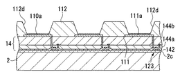
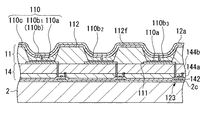
陰極形成工程では、スパッタ法により、電子注入層110cの全面にITO等の金属酸化物からなる陰極12を形成する。
スパッタターゲットには、例えばInとSnとの合金を用い、キャリアガスとして例えばアルゴン(Ar)を用いることができる。
成膜初期においては、キャリアガス中の酸素分圧を略ゼロとし、予め設定された膜厚(設定厚)だけ金属材料を成膜する。これにより、図19に示すように、電子注入層110c上に、酸素含有量が略ゼロとなる無酸素層12aが形成される。
その後、キャリアガス中の酸素分圧を連続的又は段階的に増加させながら、金属酸化物を140nm程度成膜する。これにより、図20に示すように、無酸素層12a上に、酸素を含有する有酸素層12bが形成される。
(6) Cathode Formation Step In the cathode formation step, the
For example, an alloy of In and Sn is used as a sputtering target, and argon (Ar) can be used as a carrier gas.
At the beginning of the film formation, the partial pressure of oxygen in the carrier gas is set to substantially zero, and a metal film is formed to a predetermined thickness (set thickness). Thus, as shown in FIG. 19, an oxygen-
Thereafter, a metal oxide is deposited to a thickness of about 140 nm while continuously or stepwise increasing the oxygen partial pressure in the carrier gas. Thereby, as shown in FIG. 20, an oxygen-containing
なお、設定厚(即ち、無酸素層12aの膜厚)は、5nm以上、30nm以下の範囲であることが好ましい。例えば、成膜量が5nmよりも薄い状態で酸素の供給を開始した場合には、下地の機能層(本実施形態では電子注入層110c)が酸化され、十分な発光効率が得られない。一方、無酸素層12aを30nmよりも厚く成膜した場合には、陰極12が黒ずみ、表示品質が著しく低下してしまう。
また、有酸素層12bの酸素含有量や膜厚は、無酸素層12aと有酸素層12bとを合わせた陰極12全体として十分な透明性が得られる範囲で任意に設定できる。
Note that the set thickness (that is, the thickness of the oxygen-
Further, the oxygen content and the film thickness of the oxygen-containing
(7)封止工程
封止工程は、発光素子が形成された基板2の前面に封止缶604を配置し、基板2と封止缶604の周縁部を封止樹脂603により封止する工程である。この工程により基板2上に封止部3を形成する。
封止工程は、窒素、アルゴン、ヘリウム等の不活性ガス雰囲気で行うことが好ましい。大気中で行うと、陰極12にピンホール等の欠陥が生じていた場合にこの欠陥部分から水や酸素等が陰極12に侵入して陰極12が酸化されるおそれがあるので好ましくない。また、封止缶604の内面側には、酸素や水分を吸収又は除去するゲッター材を設けることが好ましい。このゲッター材は、例えば非表示領域2bに配置し、表示に影響を及ぼさないようにすることが望ましい。
(7) Sealing Step The sealing step is a step of disposing the sealing can 604 on the front surface of the
The sealing step is preferably performed in an atmosphere of an inert gas such as nitrogen, argon, or helium. If the operation is performed in the air, if a defect such as a pinhole occurs in the
更に、図2,図3に例示した基板2の配線5aに陰極12を接続するとともに、駆動IC6に回路素子部14の配線を接続することにより、本実施形態の表示装置1が得られる。
Further, by connecting the
したがって、本実施形態のエレクトロルミネッセンス表示装置によれば、陰極12全体としての透明性を損なうことなく、陰極成膜時の機能層の酸化を効果的に防止することができる。
Therefore, according to the electroluminescent display device of the present embodiment, oxidation of the functional layer at the time of forming the cathode can be effectively prevented without impairing the transparency of the
[第2実施形態]
次に、本発明の第2の実施形態を図21を参照して説明する。なお、以下の説明では、上記第1実施形態と同様の部位については同じ符号を付し、その説明を一部省略する。また、図2、図3を適宜流用して説明する。
本実施形態のエレクトロルミネッセンス表示装置は、基板2側から順に、陰極111′、電子注入層110a′、発光層110b、正孔注入/輸送層110c′、陽極12′が順に積層された、所謂リバース構造のEL表示装置として構成されている。なお、本表示装置では、電子注入層110a′、発光層110b、正孔注入/輸送層110c′により機能層110′が構成されている。
[Second embodiment]
Next, a second embodiment of the present invention will be described with reference to FIG. In the following description, the same parts as those in the first embodiment are denoted by the same reference numerals, and the description thereof will be partially omitted. 2 and 3 will be described as appropriate.
The electroluminescent display device of the present embodiment has a so-called reverse structure in which a
また、本表示装置は、上記第1実施形態と同様に、トップエミッション型の構造を有しており、画素電極である陰極111′には、AlやAg等の高反射率の金属膜が用いられ、バンク層112及び機能層110′を覆うように形成された陽極12′にはITOやIZO等の透光性の金属酸化物が用いられている。
Further, the present display device has a top emission type structure as in the first embodiment, and a metal film having a high reflectivity such as Al or Ag is used for the
この陽極12′の酸素含有量は膜厚方向に変化しており、下層側(基板2側)が上層側(封止部3側)に比べて酸素含有量が少なくなっている。すなわち、陽極12′の平均酸素濃度は、表示に必要とされる透明性を得るために所定濃度以上に設定されるが、膜厚方向で見ると、下層側の酸素濃度が上層側の酸素濃度に比べて小さくなるように、濃度勾配が生じている。例えば、陽極12′は、酸素濃度が略ゼロである無酸素層12a′と酸素濃度が平均酸素濃度よりも大きい有酸素層12b′とが下層側から順に積層された構造を有している。このような陽極12′は、キャリアガス(例えばAr)中の酸素分圧を経時的に変化させながら、InやSn等の金属材料を正孔注入/輸送層110c′上にスパッタすることで形成される。具体的には、成膜開始直後の一定時間内(即ち、正孔注入/輸送層110c上の成膜量が所定範囲内)では、キャリアガス中の酸素分圧を略ゼロとし、その後、酸素分圧を連続的又は段階的に増加させて所望の平均酸素濃度が得られるようにしている。
The oxygen content of the
この陽極12′は、その一端が基板2上に形成された配線120に接続しており、この配線120の一端部がフレキシブル基板5上の配線5aに接続されている。また、配線5aは、フレキシブル基板5上に備えられた駆動IC6(駆動回路)に接続されている(図2,図3参照)。
そして、これ以外の構成については、上記第1実施形態と同様であるため、その説明を省略する。
One end of the
The other configuration is the same as that of the first embodiment, and a description thereof will not be repeated.
したがって、本実施形態でも、上記第1実施形態と同様に、陽極全体としての透明性を損なうことなく、キャリアガス中の活性な酸素によって機能層が酸化されることを防止することができる。 Therefore, also in the present embodiment, similarly to the first embodiment, it is possible to prevent the functional layer from being oxidized by active oxygen in the carrier gas without impairing the transparency of the entire anode.
[電子機器]
次に、上述のエレクトロルミネッセンス表示装置を備えた電子機器の例について説明する。
図22は、上述した実施形態に係る表示装置を備えたモバイル型のパーソナルコンピュータ(情報処理装置)の構成を示す斜視図である。同図において、パーソナルコンピュータ1100は、キーボード1102を備えた本体部1104と、上述したエレクトロルミネッセンス表示装置1106を備えた表示装置ユニットとから構成されている。このため、発光効率の高く明るい表示部を備えた電子機器を提供することができる。
[Electronics]
Next, an example of an electronic apparatus including the above-described electroluminescent display device will be described.
FIG. 22 is a perspective view illustrating a configuration of a mobile personal computer (information processing device) including the display device according to the above-described embodiment. In the figure, a
なお、本発明は上述の実施形態に限定されるものではなく、本発明の趣旨を逸脱しない範囲で種々変形して実施することができる。
例えば、上記実施形態では、陰極をスパッタリングで成膜する際に、成膜開始直後の酸素分圧を略ゼロとしたが、本発明はこれに限定されず、成膜開始直後の酸素分圧が、成膜中の平均の酸素分圧よりも低く設定されればよい。このようにすることで、一定の酸素分圧(即ち、上述の平均の酸素分圧)で成膜を行なう従来のものに比べて、下地の機能層110へのダメージを抑えることができる。
Note that the present invention is not limited to the above-described embodiment, and can be implemented with various modifications without departing from the spirit of the present invention.
For example, in the above embodiment, when the cathode is formed by sputtering, the oxygen partial pressure immediately after the start of the film formation is substantially zero, but the present invention is not limited to this, and the oxygen partial pressure immediately after the start of the film formation is It may be set lower than the average oxygen partial pressure during film formation. By doing so, damage to the underlying
また、上記実施形態では、R、G、Bの各発光層110bをストライプ配置した場合について説明したが、本発明はこれに限られず、様々な配置構造を採用することができる。例えば図23(a)に示すようなストライプ配置の他、図23(b)に示すようなモザイク配置や、図23(c)に示すようなデルタ配置とすることもできる。
In the above embodiment, the case where the R, G, and B
また、上記実施形態では、発光層110bに有機EL材料を用いた例を示したが、発光層110bに無機EL材料を用いたもの(即ち、無機EL表示装置)に対して本発明を適用することも勿論可能である。
さらに、上記実施形態では、隔壁112に仕切られた領域に各発光部Aを形成したが、各発光部Aを仕切る隔壁は必ずしも必要ではなく、このような隔壁112を設けない場合には、ゲッター材は、平面視で、隣接する発光部Aの間の領域に配置されていればよい。
In the above embodiment, the example in which the organic EL material is used for the
Furthermore, in the above-described embodiment, each light emitting portion A is formed in a region partitioned by the
1 エレクトロルミネッセンス表示装置、 2 基板、 2a 表示領域、
2b 非表示領域、 3 封止部、 12 陰極(第2の電極)、 110 機能層、 110b 発光層、 111 画素電極(第1の電極)、
112 バンク層(隔壁)、 123 薄膜トランジスタ(スイッチング素子)、
604 封止缶(封止部材)、 A 発光部
1 electroluminescence display device, 2 substrate, 2a display area,
2b non-display area, 3 sealing portion, 12 cathode (second electrode), 110 functional layer, 110b light emitting layer, 111 pixel electrode (first electrode),
112 bank layer (partition), 123 thin film transistor (switching element),
604 sealing can (sealing member), A light emitting unit
Claims (7)
上記第2の電極の酸素濃度は膜厚方向で変化しており、上記第2の電極と上記機能層との界面付近の酸素濃度は、上記第2の電極における平均の酸素濃度よりも低いことを特徴とする、エレクトロルミネッセンス表示装置。 On a substrate, a first electrode, a functional layer including a light-emitting layer, and a transparent second electrode made of a metal oxide are sequentially stacked from a lower layer side,
The oxygen concentration of the second electrode changes in the film thickness direction, and the oxygen concentration near the interface between the second electrode and the functional layer is lower than the average oxygen concentration in the second electrode. An electroluminescent display device characterized by the above-mentioned.
上記第1の電極上に発光層を含む機能層を形成する工程と、
酸素を含むキャリアガス雰囲気下で上記機能層上に金属材料をスパッタリングし、上記機能層上に金属酸化物からなる透明な第2の電極を形成する工程とを備え、
上記スパッタリングにおいて、上記機能層上に堆積される上記金属酸化物の堆積量が増大するに従って上記キャリアガスの酸素分圧を増大させることを特徴とする、エレクトロルミネッセンス表示装置の製造方法。 Forming a first electrode on the substrate;
Forming a functional layer including a light emitting layer on the first electrode;
Sputtering a metal material on the functional layer under a carrier gas atmosphere containing oxygen to form a transparent second electrode made of a metal oxide on the functional layer,
In the above-mentioned sputtering, a method for manufacturing an electroluminescent display device, wherein the oxygen partial pressure of the carrier gas is increased as the deposition amount of the metal oxide deposited on the functional layer is increased.
An electronic apparatus comprising the electroluminescent display device according to claim 1.
Priority Applications (6)
| Application Number | Priority Date | Filing Date | Title |
|---|---|---|---|
| JP2003344803A JP2004200146A (en) | 2002-12-05 | 2003-10-02 | Electroluminescence display device, method of manufacturing the same, and electronic apparatus |
| KR1020030077834A KR100572237B1 (en) | 2002-12-05 | 2003-11-05 | Electroluminescence display device, manufacturing method and electronic device |
| TW092131685A TWI237522B (en) | 2002-12-05 | 2003-11-12 | Electroluminescent display device, manufacturing method thereof, and electronic apparatus |
| CNB2003101181171A CN100379052C (en) | 2002-12-05 | 2003-11-13 | Electroluminescence display device, manufacturing method thereof, and electronic instrument |
| US10/722,448 US7271535B2 (en) | 2002-12-05 | 2003-11-28 | Electroluminescent display device, method for manufacturing the same, and electronic equipment |
| US11/889,178 US7641533B2 (en) | 2002-12-05 | 2007-08-09 | Electroluminescent display device, method for manufacturing the same, and electronic equipment |
Applications Claiming Priority (2)
| Application Number | Priority Date | Filing Date | Title |
|---|---|---|---|
| JP2002353672 | 2002-12-05 | ||
| JP2003344803A JP2004200146A (en) | 2002-12-05 | 2003-10-02 | Electroluminescence display device, method of manufacturing the same, and electronic apparatus |
Publications (1)
| Publication Number | Publication Date |
|---|---|
| JP2004200146A true JP2004200146A (en) | 2004-07-15 |
Family
ID=32775065
Family Applications (1)
| Application Number | Title | Priority Date | Filing Date |
|---|---|---|---|
| JP2003344803A Pending JP2004200146A (en) | 2002-12-05 | 2003-10-02 | Electroluminescence display device, method of manufacturing the same, and electronic apparatus |
Country Status (5)
| Country | Link |
|---|---|
| US (2) | US7271535B2 (en) |
| JP (1) | JP2004200146A (en) |
| KR (1) | KR100572237B1 (en) |
| CN (1) | CN100379052C (en) |
| TW (1) | TWI237522B (en) |
Cited By (8)
| Publication number | Priority date | Publication date | Assignee | Title |
|---|---|---|---|---|
| JP2005071696A (en) * | 2003-08-21 | 2005-03-17 | Sharp Corp | Organic EL device |
| JP2006040583A (en) * | 2004-07-22 | 2006-02-09 | Sharp Corp | ORGANIC ELECTROLUMINESCENT ELEMENT, ITS MANUFACTURING METHOD, AND ORGANIC ELECTROLUMINESCENT DISPLAY |
| JP2007317652A (en) * | 2006-04-28 | 2007-12-06 | Semiconductor Energy Lab Co Ltd | Method for manufacturing light emitting device |
| JP2008004361A (en) * | 2006-06-22 | 2008-01-10 | Casio Comput Co Ltd | Display device and manufacturing method thereof |
| JP2008500695A (en) * | 2004-05-25 | 2008-01-10 | エージェンシー・フォア・サイエンス・テクノロジー・アンド・リサーチ | Composite optical breakdown electrode for high-contrast electroluminescent devices |
| US20120213916A1 (en) * | 2004-01-19 | 2012-08-23 | Seiko Epson Corporation | Manufacturing method for electroluminescence display apparatus |
| US9312488B2 (en) | 2012-08-01 | 2016-04-12 | Joled Inc. | Method for manufacturing organic electroluminescent element with bi-layer cathode |
| WO2026078803A1 (en) * | 2024-10-09 | 2026-04-16 | シャープディスプレイテクノロジー株式会社 | Display device and production method therefor |
Families Citing this family (19)
| Publication number | Priority date | Publication date | Assignee | Title |
|---|---|---|---|---|
| KR101166358B1 (en) * | 2003-10-28 | 2012-07-23 | 가부시키가이샤 한도오따이 에네루기 켄큐쇼 | Method for forming wiring, method for manufacturing thin film transistor and droplet discharging method |
| JP2006201423A (en) * | 2005-01-20 | 2006-08-03 | Seiko Epson Corp | Substrate with color element, film forming method, electro-optical device, and electronic apparatus |
| US7888702B2 (en) * | 2005-04-15 | 2011-02-15 | Semiconductor Energy Laboratory Co., Ltd. | Display device and manufacturing method of the display device |
| KR101160840B1 (en) * | 2005-05-31 | 2012-06-29 | 삼성전자주식회사 | Display device and method of making the same |
| ITMI20051502A1 (en) * | 2005-07-29 | 2007-01-30 | Getters Spa | GETTER SYSTEMS INCLUDING ONE OR MORE DEPOSITS OF GETTER MATERIAL AND A LAYER OF MATERIAL FOR H02O TRANSPORT |
| US20090128024A1 (en) * | 2006-04-20 | 2009-05-21 | Kenichi Fukuoka | Organic light-emitting device |
| KR100821068B1 (en) * | 2006-05-16 | 2008-04-10 | 삼성에스디아이 주식회사 | Organic EL display device and manufacturing method thereof |
| KR100829760B1 (en) * | 2007-04-10 | 2008-05-15 | 삼성에스디아이 주식회사 | Method for manufacturing an organic light emitting device and an organic light emitting device manufactured using the same |
| US7755156B2 (en) * | 2007-12-18 | 2010-07-13 | Palo Alto Research Center Incorporated | Producing layered structures with lamination |
| US7586080B2 (en) * | 2007-12-19 | 2009-09-08 | Palo Alto Research Center Incorporated | Producing layered structures with layers that transport charge carriers in which each of a set of channel regions or portions operates as an acceptable switch |
| US8283655B2 (en) | 2007-12-20 | 2012-10-09 | Palo Alto Research Center Incorporated | Producing layered structures with semiconductive regions or subregions |
| TWI527282B (en) | 2010-09-20 | 2016-03-21 | 友達光電股份有限公司 | Light emitting unit of electroluminescence device and manufacturing method thereof |
| KR101839929B1 (en) | 2011-03-18 | 2018-03-20 | 삼성디스플레이 주식회사 | Organic light emitting display apparatus and method for manufacturing organic light emitting display apparatus |
| JPWO2014021177A1 (en) * | 2012-08-02 | 2016-07-21 | ソニー株式会社 | SEMICONDUCTOR ELEMENT, SEMICONDUCTOR ELEMENT MANUFACTURING METHOD, SOLID-STATE IMAGING DEVICE, AND ELECTRONIC DEVICE |
| CN105280680B (en) * | 2014-07-03 | 2018-10-12 | 乐金显示有限公司 | Organic LED display device and its manufacturing method |
| US9490447B2 (en) | 2014-07-03 | 2016-11-08 | Lg Display Co., Ltd. | Organic light emitting diode display device and method of fabricating the same |
| JP2016081562A (en) | 2014-10-09 | 2016-05-16 | ソニー株式会社 | Display device, display device manufacturing method, and electronic apparatus |
| KR102651060B1 (en) * | 2016-08-11 | 2024-03-26 | 삼성디스플레이 주식회사 | Organic light emitting display device |
| KR102827287B1 (en) * | 2019-01-28 | 2025-07-01 | 삼성디스플레이 주식회사 | Display device and method of manufacturing the same |
Citations (3)
| Publication number | Priority date | Publication date | Assignee | Title |
|---|---|---|---|---|
| JPH10289784A (en) * | 1997-04-14 | 1998-10-27 | Mitsubishi Chem Corp | Organic electroluminescent device |
| JP2000040589A (en) * | 1998-07-22 | 2000-02-08 | Tdk Corp | Organic EL device |
| JP2001176660A (en) * | 1999-12-20 | 2001-06-29 | Sony Corp | Method of manufacturing organic electroluminescence device and organic electroluminescence device |
Family Cites Families (12)
| Publication number | Priority date | Publication date | Assignee | Title |
|---|---|---|---|---|
| US4113599A (en) * | 1977-09-26 | 1978-09-12 | Ppg Industries, Inc. | Sputtering technique for the deposition of indium oxide |
| US5003221A (en) * | 1987-08-29 | 1991-03-26 | Hoya Corporation | Electroluminescence element |
| JP3560375B2 (en) | 1994-12-27 | 2004-09-02 | 出光興産株式会社 | Organic electroluminescent device |
| EP1452622A3 (en) * | 1995-08-23 | 2004-09-29 | Asahi Glass Ceramics Co., Ltd. | Target and process for its production, and method for forming a film having a high refractive index |
| US5760423A (en) * | 1996-11-08 | 1998-06-02 | Kabushiki Kaisha Toshiba | Semiconductor light emitting device, electrode of the same device and method of manufacturing the same device |
| US6268618B1 (en) * | 1997-05-08 | 2001-07-31 | Showa Denko K.K. | Electrode for light-emitting semiconductor devices and method of producing the electrode |
| JP3571020B2 (en) | 2000-10-17 | 2004-09-29 | 三星エスディアイ株式会社 | Organic EL device and manufacturing method thereof |
| DE10152655B4 (en) | 2000-10-17 | 2013-10-02 | Samsung Display Co., Ltd. | Process for producing an organic electroluminescent device |
| JP4066637B2 (en) | 2001-11-02 | 2008-03-26 | セイコーエプソン株式会社 | Organic electroluminescence device and electronic device |
| JP3837344B2 (en) * | 2002-03-11 | 2006-10-25 | 三洋電機株式会社 | Optical element and manufacturing method thereof |
| US7012364B2 (en) * | 2002-10-01 | 2006-03-14 | Dai Nippon Printing Co., Ltd. | Organic electroluminescent display |
| US6887799B1 (en) * | 2003-12-18 | 2005-05-03 | Sharp Laboratories Of America, Inc. | Indium oxide conductive film |
-
2003
- 2003-10-02 JP JP2003344803A patent/JP2004200146A/en active Pending
- 2003-11-05 KR KR1020030077834A patent/KR100572237B1/en not_active Expired - Fee Related
- 2003-11-12 TW TW092131685A patent/TWI237522B/en not_active IP Right Cessation
- 2003-11-13 CN CNB2003101181171A patent/CN100379052C/en not_active Expired - Fee Related
- 2003-11-28 US US10/722,448 patent/US7271535B2/en not_active Expired - Fee Related
-
2007
- 2007-08-09 US US11/889,178 patent/US7641533B2/en not_active Expired - Fee Related
Patent Citations (3)
| Publication number | Priority date | Publication date | Assignee | Title |
|---|---|---|---|---|
| JPH10289784A (en) * | 1997-04-14 | 1998-10-27 | Mitsubishi Chem Corp | Organic electroluminescent device |
| JP2000040589A (en) * | 1998-07-22 | 2000-02-08 | Tdk Corp | Organic EL device |
| JP2001176660A (en) * | 1999-12-20 | 2001-06-29 | Sony Corp | Method of manufacturing organic electroluminescence device and organic electroluminescence device |
Cited By (9)
| Publication number | Priority date | Publication date | Assignee | Title |
|---|---|---|---|---|
| JP2005071696A (en) * | 2003-08-21 | 2005-03-17 | Sharp Corp | Organic EL device |
| US20120213916A1 (en) * | 2004-01-19 | 2012-08-23 | Seiko Epson Corporation | Manufacturing method for electroluminescence display apparatus |
| US8790745B2 (en) * | 2004-01-19 | 2014-07-29 | Seiko Epson Corporation | Manufacturing method for electroluminescence display apparatus |
| JP2008500695A (en) * | 2004-05-25 | 2008-01-10 | エージェンシー・フォア・サイエンス・テクノロジー・アンド・リサーチ | Composite optical breakdown electrode for high-contrast electroluminescent devices |
| JP2006040583A (en) * | 2004-07-22 | 2006-02-09 | Sharp Corp | ORGANIC ELECTROLUMINESCENT ELEMENT, ITS MANUFACTURING METHOD, AND ORGANIC ELECTROLUMINESCENT DISPLAY |
| JP2007317652A (en) * | 2006-04-28 | 2007-12-06 | Semiconductor Energy Lab Co Ltd | Method for manufacturing light emitting device |
| JP2008004361A (en) * | 2006-06-22 | 2008-01-10 | Casio Comput Co Ltd | Display device and manufacturing method thereof |
| US9312488B2 (en) | 2012-08-01 | 2016-04-12 | Joled Inc. | Method for manufacturing organic electroluminescent element with bi-layer cathode |
| WO2026078803A1 (en) * | 2024-10-09 | 2026-04-16 | シャープディスプレイテクノロジー株式会社 | Display device and production method therefor |
Also Published As
| Publication number | Publication date |
|---|---|
| KR20040049252A (en) | 2004-06-11 |
| TWI237522B (en) | 2005-08-01 |
| CN1505446A (en) | 2004-06-16 |
| US7271535B2 (en) | 2007-09-18 |
| US7641533B2 (en) | 2010-01-05 |
| KR100572237B1 (en) | 2006-04-19 |
| CN100379052C (en) | 2008-04-02 |
| TW200417288A (en) | 2004-09-01 |
| US20050040759A1 (en) | 2005-02-24 |
| US20080274660A1 (en) | 2008-11-06 |
Similar Documents
| Publication | Publication Date | Title |
|---|---|---|
| US7641533B2 (en) | Electroluminescent display device, method for manufacturing the same, and electronic equipment | |
| JP3823916B2 (en) | Display device, electronic apparatus, and display device manufacturing method | |
| US7791269B2 (en) | Display apparatus having light blocking layer, and electric device | |
| JP3890053B2 (en) | Display device manufacturing method, display device, electronic device manufacturing method, and electronic device | |
| JP4055171B2 (en) | Color filter substrate manufacturing method, electro-optical device manufacturing method, electro-optical device, and electronic apparatus | |
| JP2004355913A (en) | Manufacturing method of organic electroluminescence device | |
| JP3951701B2 (en) | Display device manufacturing method, electronic device manufacturing method, display device, and electronic device | |
| JP2003249378A (en) | Display device and electronic equipment | |
| JP2003249355A (en) | Display device manufacturing method, display device, electronic device manufacturing method, and electronic device | |
| JP5304417B2 (en) | Display device | |
| US7449252B2 (en) | Organic electroluminescent device, manufacturing method thereof, and electronic apparatus | |
| JP4207511B2 (en) | ELECTRO-OPTICAL DEVICE, MANUFACTURING METHOD THEREOF, AND ELECTRONIC DEVICE | |
| JP2004259696A (en) | Electroluminescence device, method of manufacturing the same, and electronic device | |
| JP2003249377A (en) | Display device, electronic device, and method of manufacturing display device | |
| JP2004171862A (en) | Organic EL device manufacturing apparatus, organic EL device manufacturing method, organic EL device, and electronic apparatus | |
| JP2003217843A (en) | Display device manufacturing method, electronic device manufacturing method, display device, and electronic device | |
| JP2003282272A (en) | Electro-optical device, method of manufacturing the same, and electronic apparatus | |
| JP2005353528A (en) | Electro-optical device manufacturing method, electro-optical device, and electronic apparatus | |
| JP2005166485A (en) | ORGANIC ELECTROLUMINESCENCE DEVICE, ITS MANUFACTURING METHOD, ELECTRONIC DEVICE | |
| JP2003208978A (en) | Organic EL device manufacturing method and device, electro-optical device, and electronic apparatus |
Legal Events
| Date | Code | Title | Description |
|---|---|---|---|
| A621 | Written request for application examination |
Free format text: JAPANESE INTERMEDIATE CODE: A621 Effective date: 20050221 |
|
| A871 | Explanation of circumstances concerning accelerated examination |
Free format text: JAPANESE INTERMEDIATE CODE: A871 Effective date: 20050221 |
|
| A521 | Request for written amendment filed |
Free format text: JAPANESE INTERMEDIATE CODE: A821 Effective date: 20050222 |
|
| A131 | Notification of reasons for refusal |
Free format text: JAPANESE INTERMEDIATE CODE: A131 Effective date: 20050524 |
|
| A521 | Request for written amendment filed |
Free format text: JAPANESE INTERMEDIATE CODE: A523 Effective date: 20050721 |
|
| A975 | Report on accelerated examination |
Free format text: JAPANESE INTERMEDIATE CODE: A971005 Effective date: 20050810 |
|
| A131 | Notification of reasons for refusal |
Free format text: JAPANESE INTERMEDIATE CODE: A131 Effective date: 20050830 |
|
| A521 | Request for written amendment filed |
Free format text: JAPANESE INTERMEDIATE CODE: A523 Effective date: 20051025 |
|
| A02 | Decision of refusal |
Free format text: JAPANESE INTERMEDIATE CODE: A02 Effective date: 20060509 |