JP2004200210A - Surface emitting semiconductor laser and method of manufacturing the same - Google Patents
Surface emitting semiconductor laser and method of manufacturing the same Download PDFInfo
- Publication number
- JP2004200210A JP2004200210A JP2002363485A JP2002363485A JP2004200210A JP 2004200210 A JP2004200210 A JP 2004200210A JP 2002363485 A JP2002363485 A JP 2002363485A JP 2002363485 A JP2002363485 A JP 2002363485A JP 2004200210 A JP2004200210 A JP 2004200210A
- Authority
- JP
- Japan
- Prior art keywords
- mesa
- insulating film
- substrate
- semiconductor layers
- semiconductor laser
- Prior art date
- Legal status (The legal status is an assumption and is not a legal conclusion. Google has not performed a legal analysis and makes no representation as to the accuracy of the status listed.)
- Granted
Links
Images



Classifications
-
- H—ELECTRICITY
- H01—ELECTRIC ELEMENTS
- H01S—DEVICES USING THE PROCESS OF LIGHT AMPLIFICATION BY STIMULATED EMISSION OF RADIATION [LASER] TO AMPLIFY OR GENERATE LIGHT; DEVICES USING STIMULATED EMISSION OF ELECTROMAGNETIC RADIATION IN WAVE RANGES OTHER THAN OPTICAL
- H01S5/00—Semiconductor lasers
- H01S5/10—Construction or shape of the optical resonator, e.g. extended or external cavity, coupled cavities, bent-guide, varying width, thickness or composition of the active region
- H01S5/18—Surface-emitting [SE] lasers, e.g. having both horizontal and vertical cavities
- H01S5/183—Surface-emitting [SE] lasers, e.g. having both horizontal and vertical cavities having only vertical cavities, e.g. vertical cavity surface-emitting lasers [VCSEL]
- H01S5/18308—Surface-emitting [SE] lasers, e.g. having both horizontal and vertical cavities having only vertical cavities, e.g. vertical cavity surface-emitting lasers [VCSEL] having a special structure for lateral current or light confinement
- H01S5/18311—Surface-emitting [SE] lasers, e.g. having both horizontal and vertical cavities having only vertical cavities, e.g. vertical cavity surface-emitting lasers [VCSEL] having a special structure for lateral current or light confinement using selective oxidation
-
- H—ELECTRICITY
- H01—ELECTRIC ELEMENTS
- H01S—DEVICES USING THE PROCESS OF LIGHT AMPLIFICATION BY STIMULATED EMISSION OF RADIATION [LASER] TO AMPLIFY OR GENERATE LIGHT; DEVICES USING STIMULATED EMISSION OF ELECTROMAGNETIC RADIATION IN WAVE RANGES OTHER THAN OPTICAL
- H01S2301/00—Functional characteristics
- H01S2301/17—Semiconductor lasers comprising special layers
- H01S2301/176—Specific passivation layers on surfaces other than the emission facet
-
- H—ELECTRICITY
- H01—ELECTRIC ELEMENTS
- H01S—DEVICES USING THE PROCESS OF LIGHT AMPLIFICATION BY STIMULATED EMISSION OF RADIATION [LASER] TO AMPLIFY OR GENERATE LIGHT; DEVICES USING STIMULATED EMISSION OF ELECTROMAGNETIC RADIATION IN WAVE RANGES OTHER THAN OPTICAL
- H01S5/00—Semiconductor lasers
- H01S5/02—Structural details or components not essential to laser action
- H01S5/022—Mountings; Housings
- H01S5/02208—Mountings; Housings characterised by the shape of the housings
- H01S5/02212—Can-type, e.g. TO-CAN housings with emission along or parallel to symmetry axis
-
- H—ELECTRICITY
- H01—ELECTRIC ELEMENTS
- H01S—DEVICES USING THE PROCESS OF LIGHT AMPLIFICATION BY STIMULATED EMISSION OF RADIATION [LASER] TO AMPLIFY OR GENERATE LIGHT; DEVICES USING STIMULATED EMISSION OF ELECTROMAGNETIC RADIATION IN WAVE RANGES OTHER THAN OPTICAL
- H01S5/00—Semiconductor lasers
- H01S5/02—Structural details or components not essential to laser action
- H01S5/022—Mountings; Housings
- H01S5/02218—Material of the housings; Filling of the housings
- H01S5/02234—Resin-filled housings; the housings being made of resin
-
- H—ELECTRICITY
- H01—ELECTRIC ELEMENTS
- H01S—DEVICES USING THE PROCESS OF LIGHT AMPLIFICATION BY STIMULATED EMISSION OF RADIATION [LASER] TO AMPLIFY OR GENERATE LIGHT; DEVICES USING STIMULATED EMISSION OF ELECTROMAGNETIC RADIATION IN WAVE RANGES OTHER THAN OPTICAL
- H01S5/00—Semiconductor lasers
- H01S5/04—Processes or apparatus for excitation, e.g. pumping, e.g. by electron beams
- H01S5/042—Electrical excitation ; Circuits therefor
- H01S5/0425—Electrodes, e.g. characterised by the structure
- H01S5/04254—Electrodes, e.g. characterised by the structure characterised by the shape
-
- H—ELECTRICITY
- H01—ELECTRIC ELEMENTS
- H01S—DEVICES USING THE PROCESS OF LIGHT AMPLIFICATION BY STIMULATED EMISSION OF RADIATION [LASER] TO AMPLIFY OR GENERATE LIGHT; DEVICES USING STIMULATED EMISSION OF ELECTROMAGNETIC RADIATION IN WAVE RANGES OTHER THAN OPTICAL
- H01S5/00—Semiconductor lasers
- H01S5/10—Construction or shape of the optical resonator, e.g. extended or external cavity, coupled cavities, bent-guide, varying width, thickness or composition of the active region
- H01S5/18—Surface-emitting [SE] lasers, e.g. having both horizontal and vertical cavities
- H01S5/183—Surface-emitting [SE] lasers, e.g. having both horizontal and vertical cavities having only vertical cavities, e.g. vertical cavity surface-emitting lasers [VCSEL]
- H01S5/18358—Surface-emitting [SE] lasers, e.g. having both horizontal and vertical cavities having only vertical cavities, e.g. vertical cavity surface-emitting lasers [VCSEL] containing spacer layers to adjust the phase of the light wave in the cavity
-
- H—ELECTRICITY
- H01—ELECTRIC ELEMENTS
- H01S—DEVICES USING THE PROCESS OF LIGHT AMPLIFICATION BY STIMULATED EMISSION OF RADIATION [LASER] TO AMPLIFY OR GENERATE LIGHT; DEVICES USING STIMULATED EMISSION OF ELECTROMAGNETIC RADIATION IN WAVE RANGES OTHER THAN OPTICAL
- H01S5/00—Semiconductor lasers
- H01S5/10—Construction or shape of the optical resonator, e.g. extended or external cavity, coupled cavities, bent-guide, varying width, thickness or composition of the active region
- H01S5/18—Surface-emitting [SE] lasers, e.g. having both horizontal and vertical cavities
- H01S5/183—Surface-emitting [SE] lasers, e.g. having both horizontal and vertical cavities having only vertical cavities, e.g. vertical cavity surface-emitting lasers [VCSEL]
- H01S5/18386—Details of the emission surface for influencing the near- or far-field, e.g. a grating on the surface
- H01S5/18388—Lenses
-
- H—ELECTRICITY
- H10—SEMICONDUCTOR DEVICES; ELECTRIC SOLID-STATE DEVICES NOT OTHERWISE PROVIDED FOR
- H10W—GENERIC PACKAGES, INTERCONNECTIONS, CONNECTORS OR OTHER CONSTRUCTIONAL DETAILS OF DEVICES COVERED BY CLASS H10
- H10W72/00—Interconnections or connectors in packages
- H10W72/851—Dispositions of multiple connectors or interconnections
- H10W72/874—On different surfaces
- H10W72/884—Die-attach connectors and bond wires
Landscapes
- Physics & Mathematics (AREA)
- Condensed Matter Physics & Semiconductors (AREA)
- General Physics & Mathematics (AREA)
- Electromagnetism (AREA)
- Optics & Photonics (AREA)
- Semiconductor Lasers (AREA)
Abstract
【課題】半導体層と層間絶縁膜との剥離を抑制し、信頼性を向上させた面発光型半導体レーザを提供する。
【解決手段】基板12と、前記基板21上に積層された複数の半導体層13〜23と、前記複数の半導体層上に形成され、レーザ光の出射口を備えたメサ3と、少なくとも前記メサの側部および前記メサの周部である複数の半導体層上を被覆する層間絶縁膜24とを有し、前記メサの周部側を覆う層間絶縁膜の端部が、前記基板の切断面より内側において終端されている。
【選択図】 図1Provided is a surface-emitting type semiconductor laser in which separation between a semiconductor layer and an interlayer insulating film is suppressed and reliability is improved.
A substrate, a plurality of semiconductor layers laminated on the substrate, a mesa formed on the plurality of semiconductor layers, and provided with a laser light emission port, at least the mesa; And an interlayer insulating film 24 covering a plurality of semiconductor layers that are peripheral portions of the mesa, and an end portion of the interlayer insulating film covering the peripheral side of the mesa is closer to a cut surface of the substrate. Terminated on the inside.
[Selection diagram] Fig. 1
Description
【0001】
【発明の属する技術分野】
本発明は、通信機器、計測装置、光記録装置、画像形成装置の光源等に用いられる面発光型半導体レーザに関する。
【0002】
【従来の技術】
近年、光通信や光記録等の技術分野において、光源の二次元アレイ化が容易な表面発光型半導体レーザ(垂直共振器型表面発光レーザ;Vertical-Cavity Surface-Emitting Laser diode)への需要が増加している。このVCSEL(または、面発光レーザ)は、しきい値電流が低く消費電力が小さい、円形の光スポットが容易に得られる、ウエハ状態で評価が可能であるため生産性に優れる等、の多くの利点を有している。
【0003】
従来のVCSELチップの平面構造及び断面構造を図7に示す。図7(a)はVCSELチップ100の平面図、図7(b)は(a)のA−A線の断面図である。この面発光レーザチップ100は例えばGaAs基板105の裏面にn側電極106を備えている。GaAs基板105の表面上には、積層された複数の半導体層をエッチングして形成した柱状のポスト101が配される。図7では詳細を省略しているが、基板105上にポスト101を形成した後に、ポスト101とこの周部である露出された半導体層(例えば、AlGaAs層)を覆うように層間絶縁膜104が形成される。
【0004】
ポスト101は、ポスト構造、メサ構造、ピラー構造等と呼ばれることがある。層間絶縁膜104上には、電極パッド102及び引出し電極103が形成され、引き出し配線103がポスト101内にp側電極に電気的に接続される。
【0005】
図7に示す面発光レーザは、構造が比較的単純であるため、製造工程を簡略化することができコスト面で有利であが、この様な構造のチップを気密封止なしの状態で、高温高湿度下に置くと、水分の吸湿によりレーザ寿命が低下したり、安定した動作に不具合が生じる等の問題がある。
【0006】
吸湿性のあるAlを含む半導体層を用いた発光素子に関しては、従来から防湿あるいは耐湿について複数の提案がある。これらの提案の主なものは耐湿層を設けることで水分の浸入を防ぐものである。例えば、特許文献1ではInGaP耐湿層を用いることにより、また特許文献2ではP−GaAs表面保護層等を用いることにより吸湿を抑制する技術を開示している。
【0007】
【特許文献1】
特開2002−111054号公報
【特許文献2】
特開平11−87769号公報
【0008】
【発明が解決しようとする課題】
しかしながら、図7に示すような従来の面発光型半導体レーザには次のような課題がある。第1に、層間絶縁膜104の下地に用いたAlGaAs半導体層内のAlの吸湿性により、層間絶縁膜104が下地から剥離し、ポスト101が基板105から脱落するおそれがある。特に、図7の参照符号107で示す切断位置で基板105がダイシングされたときに、AlGaAs層と層間絶縁膜104との境界部109に、熱膨張係数等による応力により隙間が発生する場合がある。このような場合には、境界部109から水が浸入すると層間絶縁膜104の剥離が促進されてしまう。これにより、層間絶縁膜104上に形成されている電極パッド102および引き出し配線103が破損し、通電時の故障要因の一つとなってしまう。
【0009】
第2に、評価試験前後にレーザの発光が停止してしまう場合がある。図7に示した構造の面発光型半導体レーザは、ポスト101の周辺部からチップ上面全域を覆うように層間絶縁膜が広く形成される。そのために、層間絶縁膜内に過度の内部応力が生じるのが原因の1つであると推定される。
【0010】
一方、特許文献1はレーザ発振させないLEDに耐湿層を設けた構造に関するものであり、また特許文献2は埋め込み型のLED素子の構造に関するものであり。これらの技術は、図7で示すようなポスト構造の半導体レーザに適用し得るものではない。上述した層間絶縁膜の剥離や、その内部応力の発生という問題は、ポスト構造あるいはメサ型の面発型光半導体レーザに特有の課題であり、この課題については未だ十分な検討がなされていない。
【0011】
そこで、本発明は上記従来の課題を解決し、ポストあるいはメサを覆う絶縁膜との剥離を抑制し、信頼性を向上させた面発光型半導体レーザおよびその製造方法を提供することを目的とする。
さらに本発明は、絶縁膜内に発生する応力を低減し、その寿命および信頼性を向上させた面発光型半導体レーザおよびその製造方法を提供することを目的とする。
さらに本発明は、半導体層と絶縁膜との密着力を向上させて絶縁膜剥離を抑制し、信頼性および寿命を向上させた面発光型半導体レーザおよびその製造方法を提供することを目的とする。
【0012】
【課題を解決するための手段】
請求項1に記載の、面発光型半導体レーザは以下の構成を有する。基板と、前記基板上に積層された複数の半導体層と、前記複数の半導体層上に形成され、レーザ光の出射口を備えたメサと、少なくとも前記メサの側部および前記メサの周部である複数の半導体層上を被覆する絶縁膜とを有し、前記メサの周部を覆う絶縁膜の端部が、前記基板の切断面より内側において終端されている。この構成によれば、絶縁膜の端部が基板の切断面より内側において終端されていため、基板の切断面に絶縁膜と半導体層との境界面が存在せず、その境界面から水分等が浸入して絶縁膜が剥離するという事態が抑制される。絶縁膜の端部を基板の切断面より内側にするという簡単な工夫により、絶縁膜が剥離し難い構造を実現できる。
【0013】
好ましくは、請求項2に記載のように、前記切断面は前記面発光半導体レーザを形成するときのダイシング面である。また、絶縁膜の端部は、ダイシング面よりも内側にオフセットされるものでもよい。請求項2および3の構成では、絶縁膜の端部がダイシングによる影響を受けない位置まで退避されているので、ダイシング時の物理的なストレスによって絶縁膜が剥離する事態を防止することができる。
【0014】
好ましくは、前記メサの周部を覆う絶縁膜の端部は、前記メサの外径に対応する形状とすることができる。この構成では、メサの周部近傍に絶縁膜の端部が存在する構造となり、その絶縁膜の面積は小さくなる。これにより、絶縁膜の端部からの水分等の進入面積が小さくされる。
【0015】
請求項5に記載のように、前記メサは前記出射口を規定しかつ電流を注入するための電極を含み、前記電極に電気的に接続されかつ前記電極から延在された電極パッドが前記メサの周部に存する前記絶縁膜上に配され、前記絶縁膜の端部は前記電極パッドの外径に対応する形状を有してもよい。
【0016】
請求項6に記載の、面発光型半導体レーザは以下の構成を有する。基板と、前記基板上に積層された複数の半導体層と、前記複数の半導体層上に形成され、レーザ光の出射口を備えたメサと、少なくとも前記メサの側部および前記メサの周部である複数の半導体層上を被覆する絶縁膜とを有し、前記メサの周部を覆うように形成した絶縁膜に切込み部を設けるものである。この構成によれば、メサの周部含んで半導体層上を覆うように形成した絶縁膜の面積が大きな場合でも、切込み部を設けて絶縁膜を複数に分割することで、各絶縁膜内に発生する応力を分散し低減することができる。なお、複数の分割とは、絶縁膜内の応力が隣接して存在する他の絶縁膜にまで伝播し影響を与えない状態である。切込み部により絶縁膜同士が完全に分離された場合ばかりでなく、一部が接続している状態でも応力の影響を抑制できるように独立化されていればよい。
【0017】
好ましくは請求項7に記載のように、前記切込み部がメサの外径に対応する形状である。外形に対応した切り込み部を設けることで、絶縁膜への過度な内部応力が生じること防止することができる。
【0018】
好ましくは、メサは前記出射口を規定しかつ電流を注入するための電極を含み、前記電極に電気的に接続されかつ前記電極から延在された電極パッドが前記メサの周部に存する前記絶縁膜上に配され、前記切り込み部が前記電極パッドの外径に対応する形状を有してもよい。これにより、電極パッドの周辺に絶縁膜の内部応力を緩和することが可能である。
【0019】
請求項9に記載する、面発光型半導体レーザは以下の構成を有する。基板と、前記基板上に積層された複数の半導体層と、前記複数の半導体層上に形成され、レーザ光の出射口を備えたメサと、少なくとも前記メサの側部および前記メサの周部である複数の半導体層上を被覆する絶縁膜とを有し、前記複数の半導体層の一部に溝を設け、前記溝を含む領域上に前記絶縁膜が形成されている。これにより、半導体層に絶縁膜が強固に密着する構造を実現でるので、絶縁膜の剥離という事態を予防できる。
【0020】
好ましくは、前記溝が、前記メサの外径に対応する形状に配されていてもよい。これにより、メサの周部近傍に溝が形成されるので、面積の小さい絶縁膜であってもメサ基部に強く密着した構造となる。さらに絶縁膜内の内部応力も緩和する構造を実現できる。
【0021】
好ましくは、前記メサは前記出射口を規定しかつ電流を注入するための電極を含み、前記電極に電気的に接続されかつ前記電極から延在された電極パッドが前記メサの周部に存する前記絶縁膜上に配され、前記溝が前記電極パッドの外径に対応する形状を有してもよい。
【0022】
好ましくは、記絶縁膜の端部は、前記溝内で終端するようにしてもよい。これにより、電極パッドの周部に存在する絶縁膜についても半導体層への密着性を向上させることができる。
【0023】
請求項13に記載のように、メサ周部である複数の半導体層は、Alを含む半導体層を含み、前記絶縁膜が前記Alを含む半導体層上にある構造とすることができる。Alを含む半導体層は水分の吸湿性が高く絶縁膜の剥離が促進されやすいが、本発明の構造を適用することで、より効果的に絶縁膜の剥離を抑制することができる。好ましくは、Alを含む半導体層は、半導体多層構造からなる第1導電型の半導体ミラーの一部であり、AlGaAsを含む。また、メサは、少なくとも活性領域、選択酸化された領域を一部に含む電流狭窄層、および前記第1導電型と異なる第2の導電型の半導体ミラーとを含む構造を採用することができる。
【0024】
請求項15に記載のように、面発光型半導体レーザの製造方法は、基板と、前記基板上に積層された複数の半導体層と、前記複数の半導体層上に形成され、レーザ光の出射口を備えたメサと、少なくとも前記メサの側部および前記メサの周部である複数の半導体層上を被覆する絶縁膜とを有し、以下のステップを有する。絶縁膜の端部が、基板の端部より内側に終端するように、絶縁膜を除去するステップを含む。これにより、絶縁膜の剥離が抑制され、メサを基板上にしっかりと保持することできる。
【0025】
好ましくは、基板の端部は、面発光型半導体レーザの形成に際して基板をダイシングすることによって形成される切断面あるいは境界面を含む。
【0026】
請求項17に記載のように、基板と、前記基板上に積層された複数の半導体層と、前記複数の半導体層上に形成され、レーザ光の出射口を備えたメサと、少なくとも前記メサの側部および前記複数の半導体層上で前記メサの周部を含んで被覆する絶縁膜とを有する面発光型半導体レーザの製造方法であって、メサ近傍周部の絶縁膜を残して、他の絶縁膜を除去するステップとを含む。これにより、メサ近傍の絶縁膜の内部応力を緩和することができると同時に絶縁膜の剥離が抑制される。
【0027】
請求項18に記載のように、基板と、前記基板上に積層された複数の半導体層と、前記複数の半導体層上に形成され、レーザ光の出射口を備えたメサと、少なくとも前記メサの側部および前記複数の半導体層上で前記メサの周部を含んで被覆する絶縁膜とを有している面発光型半導体レーザの製造方法であって絶縁膜に切込みを形成するステップを含む。これによると、絶縁膜が切込みによって分離可能であるため、分離された絶縁膜内の内部応力が緩和される。
【0028】
請求項19に記載のように、基板と、前記基板上に積層された複数の半導体層と、前記複数の半導体層上に形成され、レーザ光の出射口を備えたメサと、少なくとも前記メサの側部および前記複数の半導体層上で前記メサの周部を含んで被覆する絶縁膜とを有する面発光型半導体レーザの製造方法であって、前記メサ形成後に、前記複数の半導体層上の一部に溝を形成するステップを含む。これにより、絶縁膜が半導体層に強力に密着しているので剥離の問題が低減される。
【0029】
好ましくは、前記製造方法はさらに、前記絶縁膜の端部が前記溝内に終端するように絶縁膜をパターンニングするステップを含むものであっても良い。
【0030】
【発明の実施の形態】
以下、図面を参照して本発明に係る複数の実施の形態を説明する。図1は本発明に係る面発光型半導体レーザの主要部を示す断面図である。図1は、それぞれの実施形態に共通の基本構造部分を示している。図1に示す基本構造部分を説明し、その後に各実施形態の特徴的な構成を順次説明する。
【0031】
本面発光レーザ1は、円筒状のメサ構造(あるいはポスト構造、ピラー構造)から成るレーザ素子部3を備えた選択酸化型の面発光型半導体レーザである。ここでは、メサ構造上に塗布される保護膜や、金属コンタクト層から延在されるボンディングパッド部等の記載を省略している。
【0032】
12はn型のGaAs基板、13はこの基板上に形成されたn型GaAsバッファ層である。基板12の裏面に形成された層11は、n側電極である。バッファ層13上の層14は、共振器の下部のn型DBR(Distributed Bragg Reflector:多層膜分布ブラッグ)層である。このn型下部DBR14は、混結比の異なる下部DBR第1ミラー層14−1と下部DBR第2ミラー層14−2とを複数積層した構造であるが、図1では第1ミラー層14−1と下部DBR第2ミラー層14−2とを模式的に示している。
【0033】
下部ミラー層14上に、下部スペーサー層15、活性領域4および上部スペーサー層18が形成されている。活性領域4は、アンドープの下部障壁層16−1、アンドープの量子井戸層17、およびアンドープの上部障壁層16−2との積層体を含む。活性領域4上には上部スペーサー層18が形成されている。上部スペーサー層18上には、p型AlGaAs層19、p型AlAs層20、p型AlGaAs層21が形成されている。AlAs層20は、その中央部に円形状の開口を規定するAlAs部20aとその周囲に選択酸化された酸化物領域20bとを含む電流狭窄層である。電流狭窄層は、そこを通る電流と光を狭窄するものである。電流狭窄層20の上下に設けた、AlGaAs層19、21は格子定数をより整合させ歪を緩和するための緩和層として機能する。これら歪緩和層は省略することができる。
【0034】
22は、共振器の上部を構成するp型の上部DBRミラー層である。上部DBRミラー層22は、混晶比の異なる上部DBR第1ミラー層22−1と上部DBR第2ミラー層22−2とを交互に複数積層して形成されるが、ここでは模式的に示している。23は、p型のコンタクト層であり、24は、層間絶縁膜、25は、コンタクト層23上に形成され出射窓を規定する環状のp側電極である。26は、p側電極25に接続された引出し電極である。
【0035】
本発明における面発光型半導体レーザでは、層間絶縁膜24の形状が特徴的である。層間絶縁膜24は、メサ構造3の上面の縁部、側面およびメサ周部の全体を被覆する。ここで、メサ周部とは、メサ3が形成されている基部から外側に延在する領域で、図1の例では下部ミラー層14上に着膜された領域24aである。従来においては、層間絶縁膜は、基板のダイシング面に至るまで基板上の全面を被覆しているが、本発明に係る層間絶縁膜24は、その形状を異にしている。
【0036】
以下、第1ないし第3の実施形態を順に説明する。図2は第1の実施形態について示した図であり、(a)は面発光半導体レーザのチップの概要を示す平面図、(b)は(a)のB−B線での断面図である。なお、この(b)で、基板12上には下部ミラー層14が存在しているがここでの図示は省略している。
【0037】
本実施形態では、チップの外周となる4辺、すなわちダイシング面107(基板の切断面)よりも、層間絶縁膜24の端部が内側に形成されている。特に、本実施形態では、層間絶縁膜24の端部を、レーザ素子部(メサ構造)3、引出し配線26及び電極パッド27の外径の応じた形状となるように、ダイシング面からオフセットされている。なお、図(a)に示す層間絶縁膜24の領域は、分かり易くするために斜線で示してある。
【0038】
層間絶縁膜24をこのように設計することで、ウエハからレーザ素子を切り落とす際に、ダイシングブレードによる機械的なストレスが層間絶縁膜24に直接加わらず、層間絶縁膜24の端部が半導体層表面(下部ミラー層14)から剥離するという事態を抑制することができる。また図2に示す例では、層間絶縁膜24の端部が、レーザ素子部3、引出し配線26及び電極パッド27の外周近傍まで大きくオフセットされ、その面積が従来と比較し大幅に縮小している。これにより、下部ミラー層14と層間絶縁膜との熱膨張係数の差等によって生じる層間絶縁膜24内の内部応力が大幅に低減される。このように、層間絶縁膜24の剥離を抑制する共に、層間絶縁膜内の応力を抑制することで、レーザの安定した動作およびその発光寿命を改善することができる。
【0039】
第1の実施態様では、層間絶縁膜24の剥離及び応力の抑制を同時に実現した構成例を示しているが、層間絶縁膜24のパターンは、図2の破線で示すような形状であっても良い。すなわち、層間絶縁膜24の端部を、ダイシング面107から内側に幾分オフセットさせたパターンとするだけで、ダイシング面107には層間絶縁膜24と下部ミラー層14との境界面が存在しないため、層間絶縁膜24の剥離の問題を解消することができる。オフセット量は、ダイシング時のブレードの加工幅を考慮して適宜選択される。
【0040】
図3を参照して第1実施形態の面発光型半導体レーザの製造方法を説明する。有機金属気相成長法(Metal Organic Chemical Vapor Deposition;MOCVD法)を用い、図3(a)で示すように先ずn型GaAs基板12上に、n型GaAsバッファ層13を積層する。バッファ層13上に、共振器の下部を構成するn型DBRミラー14層を積層する。DBR下部ミラー層14は、例えばAl0.9Ga0.1Asによる第1ミラー層14−1と、Al0.3Ga0.7Asによる第2ミラー層14−2とを、交互に40.5周期積層させて形成する。
【0041】
下部ミラー層14上に、アンドープAl0.6Ga0.4Asの下部スペーサー層15を積層し、下部スペーサー層15上にアンドープAl0.12Ga0.88Asの量子井戸層17(厚さ9nm)の上下にアンドープAl0.3Ga0.7As障壁層16−1、16−2(厚さ5nm)を設けた量子井戸活性領域4を形成する。この活性領域4上にアンドープAl0.6Ga0.4Asの上部スペーサー18層を積層し、この上部スペーサー層18上にp型Al0.9Ga0.1As層19/p型AlAs層20/p型Al0.9Ga0.1As層21を積層する。
【0042】
p型Al0.9Ga0.1As層21の上部には、共振器の上部を構成する上部DBRミラー層22が形成される。上部DBRミラー層22は、例えばアンドープAl0.3Ga0.7Asの第1ミラー層22−1と、AlAsの第2ミラー層22−2とを交互に24周期積層して形成する。上部DBRミラー層22上に、p型GaAsによるコンタクト層23を積層して、エピタキシャル成長による工程を終了する(図3(a))。
【0043】
次に、図3(b)に示すように、p型電極25をスパッタ法、蒸着法等を用いて着膜させ、フォトリソグラフィによりパターニングし、レーザ出射窓を設ける。さらにフォトリソグラフィによりレジストをパターンニングし、該レジストをマスクにRIEを行い、メサ構造を形成する。エッチングは、少なくともAlAs層20を通過する必要があるが、好ましくは下部ミラー層14が露出するまで行われる。メサ形成後、基板12を高温酸化炉に一定時間被爆させることでAlAs層20をメサ側面から酸化させ、電流狭窄層を形成する。
【0044】
図3(c)に示すように、スパッタ法、プラズマCVD法等を用いて層間絶縁膜24をまず一様に着膜させる。層間絶縁膜24の材料としては、SiNx単層膜、SiON単層膜、あるいは両者の積層構造を含んだ構成を用いていることができる。次に、フォトリソ工程によりレジストのパターンを形成し、該レジストをマスクに層間絶縁膜24の不要部分をエッチング除去する。図2で示したように、メサの周部において、レーザ素子部3、引き出し配線26および電極パッド27の形状に対応した形状となるように層間絶縁膜24を加工する。同時に、メサの表面において、p側電極25とのコンタクトのためのコンタクトホールが形成される。
【0045】
次に、リフトオフ法でTi/Auを蒸着して、引出し配線26、電極パッド27を設ける。最後に、指定通りの大きさにチップダイシング(大割)してから、裏面研磨をし、n型GaAs基板12の裏面側にAu/AuGeを蒸着してn型電極11を設け、再び個別チップにダイシングする。これで図2に示した第1実施形態のチップが完成する。
【0046】
上記のように第1実施形態に係る面発光型半導体レーザは、従来の製造工程に簡単な修正を加え、層間絶縁膜24を所定形状にエッチング加工するだけで、層間絶縁膜の剥離を抑制し、かつ層間絶縁膜の内部応力を緩和した構造を得ることができる。
【0047】
図4は第2の実施形態について示した図であり、(a)は面発光半導体レーザのチップの概要を示す平面図、(b)は(a)のC−C線での断面図である。本実施形態の層間絶縁膜24は、チップ外周の4辺(切断面)からチッピングが到達しない範囲32まで内側にオフセットされ、円柱状のレーザ素子部(メサ構造)3、引き出し配線26および電極パッド27の周辺部に存在する層間絶縁膜には切込み部31を設けている(層間絶縁膜は斜線で示してある)。
【0048】
本形態では、絶縁膜の端部がオフセットされているのでダイシング面における層間絶縁膜24の剥離を防止することができるとともに、仮に、ダイシング面から層間絶縁膜24の剥離が生じても切込み部31によりその進行を阻止することができる。さらに、切り込み部31により、レーザ素子部3の近傍に存在する層間絶縁膜24と切り込み部31を隔ててその外側に位置する層間絶縁膜24とが分離されているので、層間絶縁膜内の内部応力が相互に干渉したり、一方から他方へ伝播することが抑制される。このように、本実施の形態においても、層間絶縁膜24の剥離を抑制する共に、内部応力の発生によりメサあるいはポストが基板から脱落し、レーザ発光が停止するということを抑制することができ、レーザ素子の寿命を改善することができる。
【0049】
本実施形態に関連して、レーザ素子部3の構造に起因して生じる層間絶縁膜24内の応力を低減させたいような場合には、レーザ素子部3の周辺部にのみ切込み部31を設けたものでもよい。
【0050】
図5は本発明の第3の実施形態について示した図であり、(a)は面発光半導体レーザのチップの概要を示す平面図、(b)は(a)のD−D線での断面図である。本実施形態では、メサ3の周部である基板12の下部ミラー層14上に溝35を形成する。層間絶縁膜24の端部は、この溝35を含む領域に形成される。またその端部は溝35内において終端するものであっても良い。
【0051】
このような形態とすれば、層間絶縁膜24と下地の半導体層との接触面積が増加するので密着力が向上し、層間絶縁膜24の剥離を抑制することができる。なお、溝35の形状は、前記第1、第2の形態と同様に、レーザ素子部(メサ)3、引出し配線26、電極パッド27の近傍で、これらの形状に沿うように形成している。これにより、レーザ素子部3、引き出し配線26、および電極パッド27の形状や材質に起因して発生する層間絶縁膜24内に過度応力が生じても、それによる層間絶縁膜の破損や劣化を抑制することが可能である。また、単に層間絶縁膜24が剥離することを抑制することに対処するという観点では、チップの外周4辺の近くにこの溝35を形成してもよい。
【0052】
図5では一様に溝35が形成され、層間絶縁膜24の端部がこの溝35内に収まる例を示しているが、勿論、溝35を不連続に形成してもよい。さらに、レーザ素子部3の周部近傍にのみ層間絶縁膜24を残した場合を例示しているが、これに限らず、溝35を含む領域まで層間絶縁膜24を全面に形成しても良く、好ましくは、ダイシング面よりも手前で終端させる。
【0053】
第3の実施形態において素子を製造する場合は、メサを形成した後、露出された下部ミラー層14上に所定の形状の溝35を形成する。この溝35の形成にはドライエッチングあるいはケミカルエッチングを用いることができる。例えば硫酸系のケミカルエッチングを用いると、急激な段差がない溝部35を形成できる。この後の工程は、第1の実施形態の場合と同様であり、スパッタ法、プラズマCVD法等を用いて層間絶縁膜24を一様に着膜し、特定のマスクパターンによりフォトリソエッチングすれば図5に示す形状の層間絶縁膜24を形成できる。
【0054】
図6は、図4に示した第2の実施形態で示したチップを、TO管タイプのステム41にマウントした例を示した図である。(a)はダイマウントしたときの平面図、(b)は(a)のE−E線での断面図である。上述したように、層間絶縁膜24の一部を削除した構造としたことで、層間絶縁膜によって被覆されていない半導体層の一部が露出されてしまうので、この露出部分を外部大気から保護する必要がある
【0055】
そこで、図6ではチップをマウントしたときに、チップ40の層間絶縁膜24が露出された部分をモールド樹脂45で覆っている。チップ40の外周部分は層間絶縁膜24の端部が内側にオフセットしているが、この露出部分をモールド樹脂により保護する。これにより、チップ40の層間絶縁膜の露出部からの水等の侵入を防ぎ、更に耐湿性を改善している。
【0056】
図6に示した構造は、以下のように作製される。TO管の金属製ステム41に熱硬化型の導電性接着剤を塗布した後に、マウンタを用いてチップ40を所定の位置に加圧搭載する。これをオーブンに入れて、導電性接着剤を熱硬化させる。本例では、Ag系エポキシ接着剤を用いたが、Inソルダ、Pb系半田泊、AuSn系共晶半田も採用できる。
【0057】
次に、塗布装置により熱硬化型のモールド樹脂45を塗布し、熱硬化させる。本例ではモールド剤として低温効果型のエポキシ接着剤を用いたが、ポリイミド系材料、シリコーン樹脂系材料を同様に採用できる。次に、ボンディングワイヤ42によりチップ側の電極パッド27と外部リード線43とを接続する。ここでは、ワイヤーのキャピラリがモールド樹脂と接触しないように、チップ40上にモールド樹脂が塗布されない領域を設けている。モールド剤の高さ調整とキャピラリの軌道調整が可能な範囲でモールド剤塗布領域を適宜調整すればよい。この後にキャップをシールする工程を追加してもよい。なお、図6において、47は接地側のリード線であり、金属製ステム41を介してチップ40のn側電極と電気的に接続されている。
【0058】
なお、図6ではチップをマウントする時に、層間絶縁膜が除去した部分を樹脂で保護する例を示したが、このような対処だけでなくチップ上に、他のポリイミド等の保護膜を形成するようにしてもよい。
【0059】
以上、本発明の好ましい実施の形態について詳述したが、本発明は上記実施の形態に限定的に解釈されるべきものではなく、特許請求の範囲の構成要件を満足する範囲内で、上記実施の形態と異なる他の構成あるいは他の方法を適用することが可能である。
【0060】
【発明の効果】
以上説明したように本発明によれば、メサの側部および周部を覆う絶縁膜を基板の切断面よりも内側において終端させるようにしたことで、従来のように絶縁膜を切断面と同一させたときよりも、基板もしくは下地の半導体層から絶縁膜が剥離することが抑制され、レーザ素子部であるメサが基板から脱落したり、電極配線が切断したりすることを抑制することができ、面発光型半導体レーザを安定して動作させ、その寿命を改善することができる。さらに、絶縁膜に切欠きを設けることで、絶縁膜内に内部応力を緩和し、絶縁膜の劣化や損傷を抑制し、長寿命の面発光半導体レーザを提供できる。
【図面の簡単な説明】
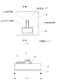
【図1】図1は本発明に係る面発光型半導体レーザの主要部を示す断面図である。
【図2】図2(a)は第1の実施形態に係る面発光半導体レーザのチップの概要を示す平面図、同(b)は(a)のB−B線での断面図である。
【図3】第1実施形態のチップの製造例を示した図である。
【図4】図4(a)は第2の実施形態に係る面発光半導体レーザのチップの概要を示す平面図、同(b)は(a)のC−C線での断面図である。
【図5】図5(a)は第3の実施形態に係る面発光半導体レーザのチップの概要を示す平面図、同(b)は(a)のD−D線での断面図である。
【図6】図4に示した第2の実施形態で示したチップを、TO管タイプのステムにダイマウントした例を示した図で、(a)はダイマウント例を示した平面図、同(b)は(a)のE−E線での断面図である。
【図7】図7(a)はVCSELチップの平面図、図7(b)は(a)のA−A線の断面図である。
【符号の説明】
1 面発光レーザ、 3 レーザ素子部(メサ)、
4 活性領域、 11 n側電極、
12 GaAs基板、 14 下部DBRミラー層、
20 電流狭窄層、 22 上部DBRミラー層、
24 層間絶縁膜、 25 p側電極
26 引き出し配線、 27 電極パッド
31 切込み部、 35 溝、
40 チップ 107 ダイシング面[0001]
TECHNICAL FIELD OF THE INVENTION
The present invention relates to a surface-emitting type semiconductor laser used for a light source of a communication device, a measuring device, an optical recording device, an image forming device, and the like.
[0002]
[Prior art]
In recent years, in the technical fields such as optical communication and optical recording, the demand for vertical-cavity surface-emitting lasers (Vertical-Cavity Surface-Emitting Laser diodes), which can easily form a two-dimensional array of light sources, has increased. are doing. This VCSEL (or surface emitting laser) has many features such as low threshold current, low power consumption, easy formation of a circular light spot, and excellent productivity because it can be evaluated in a wafer state. Has advantages.
[0003]
FIG. 7 shows a planar structure and a cross-sectional structure of a conventional VCSEL chip. 7A is a plan view of the VCSEL
[0004]
The
[0005]
The surface emitting laser shown in FIG. 7 has a relatively simple structure, so that the manufacturing process can be simplified and the cost is advantageous. However, a chip having such a structure can be obtained without hermetic sealing. When placed under high temperature and high humidity, there is a problem that the laser life is shortened due to moisture absorption or a problem occurs in stable operation.
[0006]
Regarding a light-emitting element using a semiconductor layer containing hygroscopic Al, there have conventionally been a plurality of proposals for moisture proof or moisture resistance. The main of these proposals is to prevent moisture intrusion by providing a moisture-resistant layer. For example, Patent Literature 1 discloses a technique of suppressing moisture absorption by using an InGaP moisture-resistant layer, and Patent Literature 2 discloses using a P-GaAs surface protective layer or the like.
[0007]
[Patent Document 1]
JP-A-2002-111054
[Patent Document 2]
JP-A-11-87769
[0008]
[Problems to be solved by the invention]
However, the conventional surface emitting semiconductor laser as shown in FIG. 7 has the following problems. First, due to the hygroscopicity of Al in the AlGaAs semiconductor layer used as the base of the
[0009]
Second, the laser emission may stop before and after the evaluation test. In the surface-emitting type semiconductor laser having the structure shown in FIG. 7, the interlayer insulating film is formed widely so as to cover the entire area from the periphery of the
[0010]
On the other hand, Patent Document 1 relates to a structure in which a moisture-resistant layer is provided on an LED that does not cause laser oscillation, and Patent Document 2 relates to a structure of an embedded LED element. These techniques are not applicable to a semiconductor laser having a post structure as shown in FIG. The above-mentioned problems of peeling of the interlayer insulating film and generation of internal stress thereof are problems peculiar to the post structure or the mesa-type surface-emitting type optical semiconductor laser, and this problem has not yet been sufficiently studied.
[0011]
Accordingly, it is an object of the present invention to solve the above-mentioned conventional problems, to provide a surface-emitting type semiconductor laser having improved reliability by suppressing separation from an insulating film covering a post or a mesa, and to provide a manufacturing method thereof. .
A further object of the present invention is to provide a surface-emitting type semiconductor laser in which the stress generated in an insulating film is reduced and the life and reliability thereof are improved, and a method of manufacturing the same.
Still another object of the present invention is to provide a surface-emitting type semiconductor laser in which adhesion between a semiconductor layer and an insulating film is improved to suppress peeling of the insulating film, reliability and life are improved, and a method of manufacturing the same. .
[0012]
[Means for Solving the Problems]
The surface emitting semiconductor laser according to claim 1 has the following configuration. A substrate, a plurality of semiconductor layers stacked on the substrate, a mesa formed on the plurality of semiconductor layers, and having a laser light emission port, and at least a side portion of the mesa and a peripheral portion of the mesa. An insulating film covering a plurality of semiconductor layers, and an end of the insulating film covering a periphery of the mesa is terminated inside a cut surface of the substrate. According to this configuration, since the end of the insulating film is terminated inside the cut surface of the substrate, the boundary surface between the insulating film and the semiconductor layer does not exist on the cut surface of the substrate, and moisture or the like from the boundary surface. The situation where the insulating film is separated due to intrusion is suppressed. With a simple contrivance in which the end of the insulating film is located inside the cut surface of the substrate, a structure in which the insulating film is difficult to peel can be realized.
[0013]
Preferably, the cut surface is a dicing surface when forming the surface emitting semiconductor laser. Further, the end of the insulating film may be offset inward from the dicing surface. In the configuration of the second and third aspects, since the end of the insulating film is retracted to a position not affected by the dicing, it is possible to prevent the insulating film from peeling off due to physical stress at the time of dicing.
[0014]
Preferably, an end portion of the insulating film covering a peripheral portion of the mesa may have a shape corresponding to an outer diameter of the mesa. In this configuration, the end of the insulating film exists near the periphery of the mesa, and the area of the insulating film is reduced. Thus, the area of water or the like entering from the end of the insulating film is reduced.
[0015]
6. The mesa of claim 5, wherein the mesa includes an electrode for defining the outlet and for injecting current, and an electrode pad electrically connected to and extending from the electrode. May be disposed on the insulating film existing in a peripheral portion of the electrode pad, and an end of the insulating film may have a shape corresponding to an outer diameter of the electrode pad.
[0016]
The surface emitting semiconductor laser according to claim 6 has the following configuration. A substrate, a plurality of semiconductor layers stacked on the substrate, a mesa formed on the plurality of semiconductor layers, and having a laser light emission port, and at least a side portion of the mesa and a peripheral portion of the mesa. An insulating film covering a plurality of semiconductor layers, and a cut portion is provided in the insulating film formed so as to cover the periphery of the mesa. According to this configuration, even when the area of the insulating film formed so as to cover the semiconductor layer including the peripheral portion of the mesa is large, the notch is provided to divide the insulating film into a plurality of parts, so that the inside of each insulating film is formed. The generated stress can be dispersed and reduced. Note that a plurality of divisions refers to a state in which stress in an insulating film propagates to another insulating film existing adjacently and has no effect. Not only when the insulating films are completely separated from each other by the cuts, but also when the insulating films are partially connected, the insulating films may be made independent so as to suppress the influence of stress.
[0017]
Preferably, as described in claim 7, the cut portion has a shape corresponding to the outer diameter of the mesa. By providing the cut portions corresponding to the outer shape, it is possible to prevent the occurrence of excessive internal stress on the insulating film.
[0018]
Preferably, the mesa includes an electrode for defining the emission port and injecting a current, and an electrode pad electrically connected to the electrode and extending from the electrode is provided on the periphery of the mesa. The cut portion may be provided on a film and have a shape corresponding to an outer diameter of the electrode pad. This makes it possible to reduce the internal stress of the insulating film around the electrode pad.
[0019]
The surface emitting semiconductor laser according to claim 9 has the following configuration. A substrate, a plurality of semiconductor layers stacked on the substrate, a mesa formed on the plurality of semiconductor layers and provided with a laser light emission port, and at least a side portion of the mesa and a peripheral portion of the mesa. An insulating film covering a plurality of semiconductor layers, a groove is provided in a part of the plurality of semiconductor layers, and the insulating film is formed on a region including the groove. Accordingly, a structure in which the insulating film is firmly adhered to the semiconductor layer can be realized, so that a situation in which the insulating film is separated can be prevented.
[0020]
Preferably, the groove may be arranged in a shape corresponding to an outer diameter of the mesa. As a result, a groove is formed in the vicinity of the peripheral portion of the mesa, so that even a small-area insulating film has a structure that is strongly adhered to the mesa base. Further, a structure in which the internal stress in the insulating film is also reduced can be realized.
[0021]
Preferably, the mesa includes an electrode for defining the emission port and injecting a current, and an electrode pad electrically connected to the electrode and extending from the electrode is provided on a periphery of the mesa. The groove may be provided on an insulating film, and the groove may have a shape corresponding to an outer diameter of the electrode pad.
[0022]
Preferably, an end of the insulating film may be terminated in the groove. Thereby, the adhesiveness to the semiconductor layer can be improved even for the insulating film existing around the electrode pad.
[0023]
According to a thirteenth aspect, the plurality of semiconductor layers that are peripheral portions of the mesa may include a semiconductor layer containing Al, and the insulating film may be on the semiconductor layer containing Al. Although the semiconductor layer containing Al has high moisture absorption and facilitates peeling of the insulating film, peeling of the insulating film can be more effectively suppressed by applying the structure of the present invention. Preferably, the semiconductor layer containing Al is a part of a semiconductor mirror of the first conductivity type having a semiconductor multilayer structure, and contains AlGaAs. In addition, the mesa may adopt a structure including at least an active region, a current confinement layer partially including a selectively oxidized region, and a semiconductor mirror of a second conductivity type different from the first conductivity type.
[0024]
16. A method for manufacturing a surface emitting semiconductor laser according to
[0025]
Preferably, the edge of the substrate includes a cut surface or a boundary surface formed by dicing the substrate when forming the surface emitting semiconductor laser.
[0026]
As described in
[0027]
As described in
[0028]
As described in
[0029]
Preferably, the manufacturing method may further include a step of patterning the insulating film so that an end of the insulating film ends in the groove.
[0030]
BEST MODE FOR CARRYING OUT THE INVENTION
Hereinafter, a plurality of embodiments according to the present invention will be described with reference to the drawings. FIG. 1 is a sectional view showing a main part of a surface emitting semiconductor laser according to the present invention. FIG. 1 shows a basic structure part common to each embodiment. The basic structure shown in FIG. 1 will be described, and then the characteristic configuration of each embodiment will be sequentially described.
[0031]
The surface emitting laser 1 is a selective oxidation type surface emitting semiconductor laser including a
[0032]
[0033]
On the
[0034]
Reference numeral 22 denotes a p-type upper DBR mirror layer forming the upper part of the resonator. The upper DBR mirror layer 22 is formed by alternately laminating a plurality of upper DBR first mirror layers 22-1 and upper DBR second mirror layers 22-2 having different mixed crystal ratios. ing.
[0035]
In the surface-emitting type semiconductor laser according to the present invention, the shape of the
[0036]
Hereinafter, the first to third embodiments will be sequentially described. 2A and 2B are diagrams illustrating the first embodiment, in which FIG. 2A is a plan view illustrating an outline of a chip of a surface emitting semiconductor laser, and FIG. 2B is a cross-sectional view taken along line BB of FIG. . In addition, in this (b), although the
[0037]
In the present embodiment, the edge of the
[0038]
By designing the
[0039]
In the first embodiment, a configuration example in which peeling of the
[0040]
A method for manufacturing the surface emitting semiconductor laser according to the first embodiment will be described with reference to FIG. As shown in FIG. 3A, an n-type
[0041]
On the
[0042]
p-type Al 0.9 Ga 0.1 On top of the As
[0043]
Next, as shown in FIG. 3B, the p-
[0044]
As shown in FIG. 3C, an
[0045]
Next, Ti / Au is vapor-deposited by a lift-off method to provide a
[0046]
As described above, the surface-emitting type semiconductor laser according to the first embodiment suppresses the peeling of the interlayer insulating film by simply modifying the conventional manufacturing process and etching the
[0047]
4A and 4B are diagrams showing the second embodiment, in which FIG. 4A is a plan view showing an outline of a chip of a surface emitting semiconductor laser, and FIG. 4B is a cross-sectional view taken along line CC of FIG. . The
[0048]
In this embodiment, since the end portions of the insulating film are offset, the peeling of the
[0049]
In connection with the present embodiment, when it is desired to reduce the stress in the
[0050]
5A and 5B are views showing a third embodiment of the present invention, in which FIG. 5A is a plan view showing an outline of a chip of a surface emitting semiconductor laser, and FIG. 5B is a cross section taken along line DD in FIG. FIG. In the present embodiment, a
[0051]
With such an embodiment, the contact area between the interlayer insulating
[0052]
FIG. 5 shows an example in which the
[0053]
In the case of manufacturing an element in the third embodiment, after forming a mesa, a
[0054]
FIG. 6 is a diagram showing an example in which the chip shown in the second embodiment shown in FIG. 4 is mounted on a TO
[0055]
Therefore, in FIG. 6, when the chip is mounted, a portion of the
[0056]
The structure shown in FIG. 6 is manufactured as follows. After applying a thermosetting conductive adhesive to the
[0057]
Next, a
[0058]
Although FIG. 6 shows an example in which a portion where the interlayer insulating film is removed is protected with a resin when mounting the chip, not only such measures but also a protection film such as another polyimide is formed on the chip. You may do so.
[0059]
As described above, the preferred embodiments of the present invention have been described in detail. However, the present invention should not be construed as being limited to the above-described embodiments, and the above-described embodiments may be implemented within the scope of the claims. It is possible to apply another configuration or another method different from the above-described embodiment.
[0060]
【The invention's effect】
As described above, according to the present invention, the insulating film covering the side portion and the peripheral portion of the mesa is terminated inside the cut surface of the substrate, so that the insulating film is the same as the cut surface as in the related art. In this case, the insulating film is prevented from peeling off from the substrate or the underlying semiconductor layer, and the mesa, which is the laser element, is prevented from falling off the substrate and the electrode wiring from being cut. In addition, the surface-emitting type semiconductor laser can be operated stably and its life can be improved. Furthermore, by providing a cutout in the insulating film, internal stress in the insulating film is reduced, deterioration and damage of the insulating film are suppressed, and a long-life surface emitting semiconductor laser can be provided.
[Brief description of the drawings]
FIG. 1 is a cross-sectional view showing a main part of a surface emitting semiconductor laser according to the present invention.
FIG. 2A is a plan view showing an outline of a chip of the surface emitting semiconductor laser according to the first embodiment, and FIG. 2B is a cross-sectional view taken along line BB of FIG.
FIG. 3 is a view showing an example of manufacturing the chip of the first embodiment.
FIG. 4A is a plan view illustrating an outline of a chip of a surface emitting semiconductor laser according to a second embodiment, and FIG. 4B is a cross-sectional view taken along line CC of FIG.
FIG. 5A is a plan view showing an outline of a chip of a surface emitting semiconductor laser according to a third embodiment, and FIG. 5B is a cross-sectional view taken along line DD of FIG.
6A and 6B are diagrams showing an example in which the chip shown in the second embodiment shown in FIG. 4 is die-mounted on a TO tube type stem, and FIG. 6A is a plan view showing an example of die mounting; (B) is a sectional view taken along line EE of (a).
7A is a plan view of a VCSEL chip, and FIG. 7B is a cross-sectional view taken along line AA of FIG. 7A.
[Explanation of symbols]
1 surface emitting laser, 3 laser element (mesa),
4 active region, 11 n-side electrode,
12 GaAs substrate, 14 lower DBR mirror layer,
20 current confinement layer, 22 upper DBR mirror layer,
24 interlayer insulating film, 25 p-side electrode
26 Lead wiring, 27 electrode pad
31 notches, 35 grooves,
40
Claims (20)
前記基板上に積層された複数の半導体層と、
前記複数の半導体層上に形成され、レーザ光の出射口を備えたメサと、
少なくとも前記メサの側部および前記メサの周部である複数の半導体層上を被覆する絶縁膜とを有し、
前記メサの周部を覆う絶縁膜の端部が、前記基板の切断面より内側において終端されている、面発光型半導体レーザ。Board and
A plurality of semiconductor layers stacked on the substrate,
A mesa formed on the plurality of semiconductor layers and provided with an emission port for laser light;
An insulating film that covers at least a side portion of the mesa and a plurality of semiconductor layers that are peripheral portions of the mesa,
A surface-emitting type semiconductor laser, wherein an end of an insulating film covering a periphery of the mesa is terminated inside a cut surface of the substrate.
前記基板上に積層された複数の半導体層と、
前記複数の半導体層上に形成され、レーザ光の出射口を備えたメサと、
少なくとも前記メサの側部および前記メサの周部である複数の半導体層上を被覆する絶縁膜とを有し、
前記メサの周部を覆うように形成した絶縁膜に切込み部を設けた、面発光型半導体レーザ。Board and
A plurality of semiconductor layers stacked on the substrate,
A mesa formed on the plurality of semiconductor layers and provided with an emission port for laser light;
An insulating film that covers at least a side portion of the mesa and a plurality of semiconductor layers that are peripheral portions of the mesa,
A surface-emitting type semiconductor laser, wherein a cut portion is provided in an insulating film formed so as to cover a peripheral portion of the mesa.
前記基板上に積層された複数の半導体層と、
前記複数の半導体層上に形成され、レーザ光の出射口を備えたメサと、
少なくとも前記メサの側部および前記メサの周部である複数の半導体層上を被覆する絶縁膜とを有し、
前記複数の半導体層の一部に溝を設け、前記溝を含む領域上に前記絶縁膜が形成されている、面発光型半導体レーザ。Board and
A plurality of semiconductor layers stacked on the substrate,
A mesa formed on the plurality of semiconductor layers and provided with an emission port for laser light;
An insulating film that covers at least a side portion of the mesa and a plurality of semiconductor layers that are peripheral portions of the mesa,
A surface-emitting type semiconductor laser, wherein a groove is provided in a part of the plurality of semiconductor layers, and the insulating film is formed on a region including the groove.
前記絶縁膜の端部が、前記基板の端部より内側に終端するように、前記絶縁膜を除去するステップを含む、面発光型半導体レーザの製造方法。A substrate, a plurality of semiconductor layers stacked on the substrate, a mesa formed on the plurality of semiconductor layers, and having a laser light emission port, and at least a side portion of the mesa and a peripheral portion of the mesa. A method for manufacturing a surface emitting semiconductor laser having an insulating film covering a plurality of semiconductor layers,
A method of manufacturing a surface-emitting type semiconductor laser, comprising: removing the insulating film so that an end of the insulating film is terminated inside an end of the substrate.
前記メサ近傍周部の絶縁膜を残して、他の絶縁膜を除去するステップを含む、面発光型半導体レーザの製造方法。A substrate, a plurality of semiconductor layers stacked on the substrate, a mesa formed on the plurality of semiconductor layers, and having a laser light emission port, and at least a side portion of the mesa and a peripheral portion of the mesa. A method for manufacturing a surface emitting semiconductor laser having an insulating film covering a plurality of semiconductor layers,
A method for manufacturing a surface-emitting type semiconductor laser, comprising removing another insulating film while leaving the insulating film near the mesa.
前記絶縁膜に切込みを形成するステップを含む、面発光型半導体レーザの製造方法。A substrate, a plurality of semiconductor layers stacked on the substrate, a mesa formed on the plurality of semiconductor layers, and having a laser light emission port, and at least a side portion of the mesa and a peripheral portion of the mesa. A method for manufacturing a surface emitting semiconductor laser having an insulating film covering a plurality of semiconductor layers,
A method for manufacturing a surface-emitting type semiconductor laser, comprising a step of forming a cut in the insulating film.
前記メサ形成後に、前記複数の半導体層上の一部に溝を形成するステップを含む、面発光型半導体レーザの製造方法。A substrate, a plurality of semiconductor layers stacked on the substrate, a mesa formed on the plurality of semiconductor layers, and having a laser light emission port, and at least a side portion of the mesa and a peripheral portion of the mesa. A method for manufacturing a surface emitting semiconductor laser having an insulating film covering a plurality of semiconductor layers,
A method for manufacturing a surface-emitting type semiconductor laser, comprising a step of forming a groove in a part of the plurality of semiconductor layers after forming the mesa.
Priority Applications (4)
| Application Number | Priority Date | Filing Date | Title |
|---|---|---|---|
| JP2002363485A JP4507489B2 (en) | 2002-12-16 | 2002-12-16 | Surface emitting semiconductor laser and manufacturing method thereof |
| US10/639,645 US20040114653A1 (en) | 2002-12-16 | 2003-08-13 | Surface emitting semiconductor laser and method of fabricating the same |
| CN2005101051726A CN1741332B (en) | 2002-12-16 | 2003-09-15 | Surface-emitting semiconductor laser and its manufacturing method |
| CNB03156934XA CN100524984C (en) | 2002-12-16 | 2003-09-15 | Surface emitting semiconductor laser and method of manufacturing the same |
Applications Claiming Priority (1)
| Application Number | Priority Date | Filing Date | Title |
|---|---|---|---|
| JP2002363485A JP4507489B2 (en) | 2002-12-16 | 2002-12-16 | Surface emitting semiconductor laser and manufacturing method thereof |
Publications (2)
| Publication Number | Publication Date |
|---|---|
| JP2004200210A true JP2004200210A (en) | 2004-07-15 |
| JP4507489B2 JP4507489B2 (en) | 2010-07-21 |
Family
ID=32501081
Family Applications (1)
| Application Number | Title | Priority Date | Filing Date |
|---|---|---|---|
| JP2002363485A Expired - Fee Related JP4507489B2 (en) | 2002-12-16 | 2002-12-16 | Surface emitting semiconductor laser and manufacturing method thereof |
Country Status (3)
| Country | Link |
|---|---|
| US (1) | US20040114653A1 (en) |
| JP (1) | JP4507489B2 (en) |
| CN (2) | CN1741332B (en) |
Cited By (11)
| Publication number | Priority date | Publication date | Assignee | Title |
|---|---|---|---|---|
| JP2006339418A (en) * | 2005-06-02 | 2006-12-14 | Seiko Epson Corp | Optical element and manufacturing method thereof |
| JP2007123738A (en) * | 2005-10-31 | 2007-05-17 | Sony Corp | Optical transmission module, optical transmission / reception module, and optical communication device |
| JP2007150237A (en) * | 2005-10-26 | 2007-06-14 | Seiko Epson Corp | Optical element and manufacturing method thereof |
| JP2008004670A (en) * | 2006-06-21 | 2008-01-10 | Seiko Epson Corp | Electrode structure and optical semiconductor device |
| JP2009147287A (en) * | 2007-11-20 | 2009-07-02 | Fuji Xerox Co Ltd | Surface emitting semiconductor laser array device with improved reliability by stress control of interlayer insulating film |
| JP2010258054A (en) * | 2009-04-22 | 2010-11-11 | Fuji Xerox Co Ltd | Surface emitting semiconductor laser, surface emitting semiconductor laser device, optical transmission device, optical information processing device, and method of manufacturing surface emitting semiconductor laser |
| US7957447B2 (en) | 2007-11-20 | 2011-06-07 | Fuji Xerox Co., Ltd. | VCSEL array device and method for manufacturing the VCSEL array device |
| KR101111720B1 (en) | 2005-10-12 | 2012-02-15 | 삼성엘이디 주식회사 | Side-emitting semiconductor laser diode with a dielectric layer formed on the active layer |
| US8243767B2 (en) | 2005-11-29 | 2012-08-14 | Fuji Xerox Co., Ltd. | Vertical-cavity surface-emitting laser (VCSEL) device and the method of manufacturing thereof |
| US10128633B2 (en) | 2017-03-17 | 2018-11-13 | Sumitomo Electric Industries, Ltd. | Surface emitting semiconductor laser |
| US20200412100A1 (en) * | 2019-06-28 | 2020-12-31 | Seiko Epson Corporation | Light emitting device and projector |
Families Citing this family (5)
| Publication number | Priority date | Publication date | Assignee | Title |
|---|---|---|---|---|
| EP2054980B1 (en) * | 2006-08-23 | 2013-01-09 | Ricoh Company, Ltd. | Surface-emitting laser array, optical scanning device, and image forming device |
| JP4639249B2 (en) * | 2008-07-31 | 2011-02-23 | キヤノン株式会社 | Surface emitting laser manufacturing method, surface emitting laser array manufacturing method, surface emitting laser, surface emitting laser array, and optical apparatus including surface emitting laser array |
| TWI427879B (en) * | 2010-12-22 | 2014-02-21 | Univ Nat Central | Vertical Resonant Cavity with Infrared Profile |
| JP6323650B2 (en) * | 2013-12-20 | 2018-05-16 | セイコーエプソン株式会社 | Surface emitting laser and atomic oscillator |
| CN108923261B (en) * | 2018-10-24 | 2019-01-29 | 常州纵慧芯光半导体科技有限公司 | Dot structure of vertical cavity surface emitting laser and preparation method thereof |
Citations (6)
| Publication number | Priority date | Publication date | Assignee | Title |
|---|---|---|---|---|
| JPS5630777A (en) * | 1979-08-21 | 1981-03-27 | Stanley Electric Co Ltd | Manufacture of light emitting diode chip |
| JPH0359811A (en) * | 1989-07-28 | 1991-03-14 | Hitachi Ltd | Thin-film magnetic head and production thereof |
| JP2000232250A (en) * | 1999-02-10 | 2000-08-22 | Furukawa Electric Co Ltd:The | Long wavelength band surface emitting laser device and manufacturing method thereof |
| JP2001015860A (en) * | 1999-04-26 | 2001-01-19 | Fujitsu Ltd | Semiconductor light emitting device and method of manufacturing the same |
| JP2001168282A (en) * | 1999-12-09 | 2001-06-22 | Nec Corp | Semiconductor integrated circuit and its manufacture method |
| JP2001284702A (en) * | 2000-03-30 | 2001-10-12 | Seiko Epson Corp | Optical transmission module and surface emitting laser used therein |
Family Cites Families (9)
| Publication number | Priority date | Publication date | Assignee | Title |
|---|---|---|---|---|
| JPH02155278A (en) * | 1988-12-08 | 1990-06-14 | Ricoh Co Ltd | Optically functional element |
| JPH06301990A (en) * | 1993-04-12 | 1994-10-28 | Rohm Co Ltd | Light pickup |
| US5513202A (en) * | 1994-02-25 | 1996-04-30 | Matsushita Electric Industrial Co., Ltd. | Vertical-cavity surface-emitting semiconductor laser |
| JP2783210B2 (en) * | 1995-09-04 | 1998-08-06 | 日本電気株式会社 | Surface-emitting diode |
| US6185238B1 (en) * | 1997-02-21 | 2001-02-06 | Kabushiki Kaisha Toshiba | Nitride compound semiconductor laser and its manufacturing method |
| US6107647A (en) * | 1997-05-15 | 2000-08-22 | Rohm Co. Ltd. | Semiconductor AlGaInP light emitting device |
| JP2000261029A (en) * | 1999-03-12 | 2000-09-22 | Oki Electric Ind Co Ltd | Optical semiconductor element |
| JP2001068789A (en) * | 1999-08-26 | 2001-03-16 | Fuji Photo Film Co Ltd | Semiconductor laser |
| US6777253B2 (en) * | 2000-12-20 | 2004-08-17 | Matsushita Electric Industrial Co., Ltd. | Method for fabricating semiconductor, method for fabricating semiconductor substrate, and semiconductor light emitting device |
-
2002
- 2002-12-16 JP JP2002363485A patent/JP4507489B2/en not_active Expired - Fee Related
-
2003
- 2003-08-13 US US10/639,645 patent/US20040114653A1/en not_active Abandoned
- 2003-09-15 CN CN2005101051726A patent/CN1741332B/en not_active Expired - Lifetime
- 2003-09-15 CN CNB03156934XA patent/CN100524984C/en not_active Expired - Lifetime
Patent Citations (6)
| Publication number | Priority date | Publication date | Assignee | Title |
|---|---|---|---|---|
| JPS5630777A (en) * | 1979-08-21 | 1981-03-27 | Stanley Electric Co Ltd | Manufacture of light emitting diode chip |
| JPH0359811A (en) * | 1989-07-28 | 1991-03-14 | Hitachi Ltd | Thin-film magnetic head and production thereof |
| JP2000232250A (en) * | 1999-02-10 | 2000-08-22 | Furukawa Electric Co Ltd:The | Long wavelength band surface emitting laser device and manufacturing method thereof |
| JP2001015860A (en) * | 1999-04-26 | 2001-01-19 | Fujitsu Ltd | Semiconductor light emitting device and method of manufacturing the same |
| JP2001168282A (en) * | 1999-12-09 | 2001-06-22 | Nec Corp | Semiconductor integrated circuit and its manufacture method |
| JP2001284702A (en) * | 2000-03-30 | 2001-10-12 | Seiko Epson Corp | Optical transmission module and surface emitting laser used therein |
Cited By (12)
| Publication number | Priority date | Publication date | Assignee | Title |
|---|---|---|---|---|
| JP2006339418A (en) * | 2005-06-02 | 2006-12-14 | Seiko Epson Corp | Optical element and manufacturing method thereof |
| KR101111720B1 (en) | 2005-10-12 | 2012-02-15 | 삼성엘이디 주식회사 | Side-emitting semiconductor laser diode with a dielectric layer formed on the active layer |
| JP2007150237A (en) * | 2005-10-26 | 2007-06-14 | Seiko Epson Corp | Optical element and manufacturing method thereof |
| JP2007123738A (en) * | 2005-10-31 | 2007-05-17 | Sony Corp | Optical transmission module, optical transmission / reception module, and optical communication device |
| US8243767B2 (en) | 2005-11-29 | 2012-08-14 | Fuji Xerox Co., Ltd. | Vertical-cavity surface-emitting laser (VCSEL) device and the method of manufacturing thereof |
| JP2008004670A (en) * | 2006-06-21 | 2008-01-10 | Seiko Epson Corp | Electrode structure and optical semiconductor device |
| JP2009147287A (en) * | 2007-11-20 | 2009-07-02 | Fuji Xerox Co Ltd | Surface emitting semiconductor laser array device with improved reliability by stress control of interlayer insulating film |
| US7957447B2 (en) | 2007-11-20 | 2011-06-07 | Fuji Xerox Co., Ltd. | VCSEL array device and method for manufacturing the VCSEL array device |
| JP2010258054A (en) * | 2009-04-22 | 2010-11-11 | Fuji Xerox Co Ltd | Surface emitting semiconductor laser, surface emitting semiconductor laser device, optical transmission device, optical information processing device, and method of manufacturing surface emitting semiconductor laser |
| US10128633B2 (en) | 2017-03-17 | 2018-11-13 | Sumitomo Electric Industries, Ltd. | Surface emitting semiconductor laser |
| US20200412100A1 (en) * | 2019-06-28 | 2020-12-31 | Seiko Epson Corporation | Light emitting device and projector |
| US11575247B2 (en) * | 2019-06-28 | 2023-02-07 | Seiko Epson Corporation | Light emitting device and projector |
Also Published As
| Publication number | Publication date |
|---|---|
| CN1741332B (en) | 2012-05-23 |
| US20040114653A1 (en) | 2004-06-17 |
| CN1508916A (en) | 2004-06-30 |
| CN1741332A (en) | 2006-03-01 |
| CN100524984C (en) | 2009-08-05 |
| JP4507489B2 (en) | 2010-07-21 |
Similar Documents
| Publication | Publication Date | Title |
|---|---|---|
| JP5947293B2 (en) | Manufacturing method for optoelectronic components | |
| JP4507489B2 (en) | Surface emitting semiconductor laser and manufacturing method thereof | |
| USRE44163E1 (en) | Semiconductor light emitting device and method for manufacturing the same | |
| US9172213B2 (en) | VCSEL module and manufacture thereof | |
| JP3540605B2 (en) | Light emitting element | |
| JP6074317B2 (en) | Semiconductor light emitting device and light source unit | |
| US20100260227A1 (en) | Semiconductor laser apparatus and fabrication method thereof | |
| JP3896704B2 (en) | GaN compound semiconductor light emitting device | |
| JP5759004B2 (en) | Optoelectronic semiconductor chip | |
| JP5148336B2 (en) | Light emitting diode chip and manufacturing method thereof | |
| JPH11354888A (en) | Semiconductor light emitting device and method of manufacturing the same | |
| US20030010989A1 (en) | Light-emitting diode array | |
| CN113711366B (en) | Optical semiconductor element, optical semiconductor device, optical transmission system, and method for manufacturing optical semiconductor device | |
| JPH10223930A (en) | Semiconductor light emitting device | |
| JP2017054902A (en) | Semiconductor light emitting device | |
| US6584135B2 (en) | Vertical cavity surface emitting laser diode and method for manufacturing same | |
| US20070091962A1 (en) | Substrate for vertical cavity surface emitting laser ( VCSEL) and method for manufacturing VCSEL device | |
| US7463662B2 (en) | Optical semiconductor device, manufacturing method therefor, and optical semiconductor apparatus | |
| US7817694B2 (en) | Semiconductor laser apparatus and manufacturing method thereof | |
| JP2021009895A (en) | Surface emitting laser | |
| US6660550B2 (en) | Surface emission type semiconductor light-emitting device and method of manufacturing the same | |
| JP4885434B2 (en) | Semiconductor laser device, optical disk device, and optical transmission system | |
| JP2014150225A (en) | Semiconductor light-emitting element | |
| JP2012054474A (en) | Semiconductor laser device | |
| JP4879094B2 (en) | Semiconductor light emitting device and manufacturing method thereof |
Legal Events
| Date | Code | Title | Description |
|---|---|---|---|
| A621 | Written request for application examination |
Free format text: JAPANESE INTERMEDIATE CODE: A621 Effective date: 20051122 |
|
| A977 | Report on retrieval |
Free format text: JAPANESE INTERMEDIATE CODE: A971007 Effective date: 20080708 |
|
| A131 | Notification of reasons for refusal |
Free format text: JAPANESE INTERMEDIATE CODE: A131 Effective date: 20080917 |
|
| A521 | Request for written amendment filed |
Free format text: JAPANESE INTERMEDIATE CODE: A523 Effective date: 20081117 Free format text: JAPANESE INTERMEDIATE CODE: A821 Effective date: 20081117 |
|
| A131 | Notification of reasons for refusal |
Free format text: JAPANESE INTERMEDIATE CODE: A131 Effective date: 20090804 |
|
| A521 | Request for written amendment filed |
Free format text: JAPANESE INTERMEDIATE CODE: A523 Effective date: 20090924 Free format text: JAPANESE INTERMEDIATE CODE: A821 Effective date: 20090924 |
|
| TRDD | Decision of grant or rejection written | ||
| A01 | Written decision to grant a patent or to grant a registration (utility model) |
Free format text: JAPANESE INTERMEDIATE CODE: A01 Effective date: 20100413 |
|
| A01 | Written decision to grant a patent or to grant a registration (utility model) |
Free format text: JAPANESE INTERMEDIATE CODE: A01 |
|
| A61 | First payment of annual fees (during grant procedure) |
Free format text: JAPANESE INTERMEDIATE CODE: A61 Effective date: 20100426 |
|
| FPAY | Renewal fee payment (event date is renewal date of database) |
Free format text: PAYMENT UNTIL: 20130514 Year of fee payment: 3 |
|
| R150 | Certificate of patent or registration of utility model |
Ref document number: 4507489 Country of ref document: JP Free format text: JAPANESE INTERMEDIATE CODE: R150 Free format text: JAPANESE INTERMEDIATE CODE: R150 |
|
| FPAY | Renewal fee payment (event date is renewal date of database) |
Free format text: PAYMENT UNTIL: 20140514 Year of fee payment: 4 |
|
| LAPS | Cancellation because of no payment of annual fees |