JP2004200260A - Method for manufacturing flexible rigid build-up multilayer wiring board - Google Patents
Method for manufacturing flexible rigid build-up multilayer wiring board Download PDFInfo
- Publication number
- JP2004200260A JP2004200260A JP2002364591A JP2002364591A JP2004200260A JP 2004200260 A JP2004200260 A JP 2004200260A JP 2002364591 A JP2002364591 A JP 2002364591A JP 2002364591 A JP2002364591 A JP 2002364591A JP 2004200260 A JP2004200260 A JP 2004200260A
- Authority
- JP
- Japan
- Prior art keywords
- build
- layer
- wiring board
- flexible rigid
- manufacturing
- Prior art date
- Legal status (The legal status is an assumption and is not a legal conclusion. Google has not performed a legal analysis and makes no representation as to the accuracy of the status listed.)
- Pending
Links
Images

Landscapes
- Production Of Multi-Layered Print Wiring Board (AREA)
Abstract
【課題】フレキシブルリジッドプリント配線板への積層後にビルドアップ層の一部を剥離する必要のない、フレキシブルリジッドビルドアップ配線板の製造方法を提供する。
【解決手段】フレキシブルリジッドプリント配線板(20)への積層に先だって、ビルドアップ層(27)を加工して、フレキシブルリジッドプリント配線板(20)のケーブル接続部(26)とする部位に対応する部分(29)を除去しておく。ビルドアップ層(27)の材料としてはローフロータイプの樹脂を用いる。
【選択図】 図3Provided is a method for manufacturing a flexible rigid build-up wiring board which does not require a part of a build-up layer to be peeled off after lamination on a flexible rigid printed wiring board.
Prior to lamination on a flexible rigid printed wiring board (20), a build-up layer (27) is processed to correspond to a portion to be a cable connection part (26) of the flexible rigid printed wiring board (20). The part (29) has been removed. A low flow type resin is used as a material for the build-up layer (27).
[Selection diagram] FIG.
Description
【0001】
【発明の属する技術分野】
本発明は、微細な回路の形成等の為に、フレキシブルリジッドプリント配線板にビルドアップ層が積層されたフレキシブルリジッドビルドアップ配線板の製造方法に関し、特に屈曲性を有するFPCケーブル部での接続の為に、ビルドアップ層の一部が除去されたフレキシブルリジッドビルドアップ配線板の製造方法に関する。
【0002】
【従来の技術】
フレキシブルリジッドビルドアップ配線板は、通常、フレキシブルリジッドプリント配線板をコア材(内層)として使用し、外層としてビルドアップ絶縁樹脂に銅めっきを施したもの、あるいは、ビルドアップ絶縁樹脂に銅箔が設けられたRCC(ビルドアップ絶縁樹脂付き銅箔の略)のものが主流となっている(以下、ビルドアップ絶縁樹脂に金属めっきあるいは金属箔を付けたものを総称して、ビルドアップ層という)。
【0003】
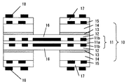
図1は、従来のフレキシブルリジッドビルドアップ配線板の一例を示す断面図である。このフレキシブルリジッドビルドアップ配線板は、フレキシブルリジッド配線板10をコア材として、このフレキシブルリジッド配線板10に外層としてのビルドアップ層17が積層されている。フレキシブルリジッド配線板10は、FPC(フレキシブル基板)基材11とFPC基材11の両面それぞれに設けられたポリイミド系樹脂を主体としたフィルムカバーレイ12と、各フィルムカバーレイ12の中央部を露出させた状態で、接着剤層13を介して各フィルムカバーレイ12上に積層されたガラスエポキシ樹脂層14とを有している。
【0004】
フレキシブルリジッドプリント配線板10のFPC基材11は、ベースフィルム11aの両面に銅めっき等で導体11bをそれぞれ形成して構成されている。フレキシブルリジッドプリント配線板10は、FPC基材11の両面をそれぞれ被覆するフィルムカバーレイ12と、各フィルムカバーレイ12の中央部を露出させた状態で、接着剤層13を介して各フィルムカバーレイ12上に積層されたガラスエポキシ樹脂層14と、各ガラスエポキシ樹脂14に、回路を形成するように設けられた銅めっき等の導体15を有している。このようなフレキシブルリジッドプリント配線板10は、FPC基材11の両面それぞれに1層の配線構造を有する。
【0005】
フレキシブルリジッドプリント配線板10の各ガラスエポキシ樹脂層14上には、導体15を覆うようにビルドアップ層17が積層されて、さらに最外層に導体18が銅箔あるいは銅めっきにより形成され、フレキシブルリジッドビルドアップ配線板が構成されている。フレキシブルリジッドビルドアップ配線板は、FPC基材11の両面それぞれに2層の積層配線構造を有する。
【0006】
フレキシブルリジッドプリント配線板10におけるガラスエポキシ樹脂層14が積層されていない各フィルムカバーレイ12中央部には、FPCが接続されるケーブル接続部16が形成されている。各ケーブル接続部16上には、ビルドアップ層17が積層されず、結果として、ガラスエポキシ樹脂層14から露出した状態になっている。
【0007】
このような構成のフレキシブルリジッドビルドアップ配線板は、通常、フォトビア法あるいはレーザー法によって製造される。特開平11−26945号公報には、フォトビア法によるフレキシブルリジッドビルドアップ配線板の製造方法が開示されている。
【0008】
フォトビア法によってフレキシブルリジッドビルドアップ配線板を製造する場合、まず、フレキシブルリジッドプリント配線板10を準備する。フレキシブルリジッドプリント配線板10は、ベースフィルム11aの両面に導体11bを設けてFPC基材11とし、そのFPC基材11の両面にポリイミド系樹脂を主体とするフィルムカバーレイ12を積層し、各フィルムカバーレイ12の中央部を露出させた状態で、接着剤層13を介して各フィルムカバーレイ12上にガラスエポキシ樹脂層14を積層して作製する。
【0009】
フレキシブルリジッドプリント配線板10を準備した後、各ガラスエポキシ樹脂層14の外層側に導体15によって回路を形成する。
【0010】
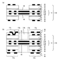
次に、各ガラスエポキシ樹脂層14のうち、各側部にて挟まれた中央部のみを、金型打ち抜きによって選択的に除去して、図2(a)に示すように、フレキシブルリジッドプリント配線板10の各ケーブル接続部16をそれぞれ露出させる。このような状態とした後、図2(b)に示すように、各ガラスエポキシ樹脂層14上の導体15をエッチングするとともに、各ケーブル接続部16を埋めるように、フレキシブルリジッドプリント配線板10上にビルドアップ層17を積層する。各ビルドアップ層17は、感光性を有する樹脂によって構成し、各ビルドアップ層17の表面は平坦に形成しておく。
【0011】
その後、各ビルドアップ層17に紫外線を選択的に照射して、ビルドアップ層17のリジッド部17cに70〜150μm程度の直径をもつブラインドバイアホール19が形成されるように、かつ、ガラスエポキシ樹脂層14に近接した側縁部17aのみが除去されて中央部17bが残存するように、各ビルドアップ層17を選択的に薬液処理する。このとき、各中央部17bによって被膜されているケーブル接続部16上は、薬液処理によって損傷する恐れがない。次に、銅箔あるいは銅めっきにより導体18を形成し、ソルダーレジスト形成、表面処理を順次実施し、さらに、各ケーブル接続16の上に残ったビルドアップ層17の中央部17bを除去して、各ケーブル接続部16の全てを露出させる。これにより、図1に示すフレキシブルリジッドビルドアップ配線板が得られる。
【0012】
このようなフレキシブルリジッドビルドアップ配線板の作製方法において、近年、レーザーを用いたビルドアップ層のブラインドバイアホール形成が、レーザー装置の高速化、安定化により、主流となりつつある。レーザー法によってブランドバイアホール19を形成する場合、ビルドアップ層17のリジッド部17cの所定位置に対してレーザー光を照射する。また、ケーブル接続部16上のビルドアップ層17を、積層後に剥離して、ケーブル接続部16を露出させる。なお、このようなビルドップ層17のリジッド部17c上のブラインドバイアホール形成のレーザー光としては、炭酸ガスレーザー、UV−YAGレーザー等が主に使用される。
【0013】
【特許文献1】特開平11−26945号公報
【0014】
【発明が解決しようとする課題】
一般に、リジッドビルドアップ配線板の場合のビルドアップ層は、内層回路への埋め込み性を良好にする為に、積層時の加圧・加熱によって樹脂が回路間に完全に流動し(以下、流動をフローと称す)、絶縁性を確保する事が必須条件となっている。一方、フレキシブルリジッドビルドアップ配線板の場合のビルドアップ層においては、上記必須条件に加えて、ケーブル接続部16を開口させる為に、ケーブル接続部16上のフローしたビルドアップ層を何らかの方法で後に剥離する工程が必要となる。この剥離工程は、コスト、作業時間共に多大なものとなっているのが現状であり、省略できることが望ましい。
【0015】
剥離工程を省略するためには、内層回路への樹脂の埋め込み性を確保する条件に加えて、ケーブル接続部16上に樹脂がフローせずに開口した状態にするという条件が求められる。ところが、通常のビルドアップ層に使用される樹脂では、この要求を満足する事が出来ず、従来の製造方法を踏襲するならば、新たにフローの制御出来る樹脂の開発が必要となる。
【0016】
本発明はこのような問題点に鑑みてなされたもので、フレキシブルリジッドプリント配線板への積層後にビルドアップ層の一部を剥離する必要のない、フレキシブルリジッドビルドアップ配線板の製造方法を提供することを目的とする。
【0017】
【課題を解決するための手段】
上記目的を達成するために、本発明では、フレキシブルリジッドプリント配線板に、その一部が露出するように、ビルドアップ層が積層されたフレキシブルリジッドビルドアップ配線板の製造方法は、フレキシブルリジッドプリント配線板への積層前のビルドアップ層を加工して、フレキシブルリジッドプリント配線板の露出する部位に相当する部位を除去する除去加工工程と、フレキシブルリジッドプリント配線板にビルドアップ層を積層する積層工程と、層間接続のためにビルドアップ層をレーザーによって加工するレーザー加工工程と、レーザー加工工程の後の残留物を薬液によって除去する薬液処理工程とを包含するものとする。
【0018】
この製造方法では、フレキシブルリジッドプリント配線板に積層する前に、ビルドアップ層を加工して配線板を露出させるための部位を除去しておく。したがって、フレキシブルリジッドプリント配線板からビルドアップ層の一部を剥離する工程は不要である。しかも、ビルドアップ層の材料とて、特にフロー制御の容易な樹脂を用いる必要がなく、従来のローフロータイプの樹脂を使用することができる。
【0019】
除去加工工程では、金型加工を採用することができるし、ルータ加工を採用することもできる。
【0020】
ビルドアップ層は、低流動性の絶縁樹脂層上に金属箔を設けることによっても、低流動性の絶縁樹脂層に金属メッキを施すことによっても、作製することができる。
【0021】
また、積層工程の後かつ薬液処理工程の前に、ビルドアップ層とフレキシブルリジッドプリント配線板とを貫通するスルーホールを形成する貫通加工工程を包含し、薬液処理工程において、レーザー加工工程と貫通加工工程の後の残留物を同じ薬液で一度に処理するようにすることもできる。
【0022】
【発明の実施の形態】
以下、本発明のいくつかの実施形態について、図面を参照しながら説明する。なお、各実施形態は例示にすぎず、本発明はこれらの実施形態に限定されるものではない。
【0023】
<第1の実施形態>
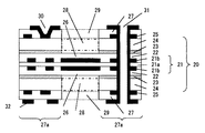
図3は、本発明のフレキシブルリジッドビルドアップ配線板の製造方法の一工程を示す断面図である。本実施形態では、図1に示すフレキシブルリジッドビルドアップ配線板と同様のフレキシブルリジッドビルドアップ配線板を製造する。
【0024】
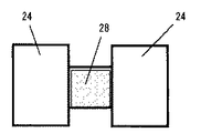
まず、フレキシブルリジッドプリント配線板20を準備する。フレキシブルリジッドプリント配線板20は、ベースフィルム21aの両面それぞれに導体21bを設けてFPC基材21とし、このFPC基材21の両面それぞれにポリイミド系樹脂を主体とするフィルムカバーレイ22を積層し、各フィルムカバーレイ22の中央部を露出させた状態で、各フィルムカバーレイ22上に接着剤層23を介してガラスエポキシ樹脂層24を積層して作製する。
【0025】
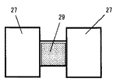
ここで、フレキシブルリジッドプリント配線板20のFPCケーブル部上に相当するガラスエポキシ樹脂層24の部分は、積層前に、金型あるいはルーターにてくり貫いておく。図3において鎖線で示した領域28が、ガラスエポキシ樹脂層24のくり貫かれた部分に該当する。図4にガラスエポキシ樹脂層24の平面図を示す。このように、ガラスエポキシ樹脂層24のうち、FPCケーブル上に位置する領域28を、FPC基材21への積層前に加工して除去しておく。
【0026】
フレックスリジッドプリント配線板20の作成後、各ガラスエポキシ樹脂層24の表面に導体25によって回路を形成する。
【0027】
次に、ビルドアップ樹脂及び銅箔からなるRCCにてビルドアップ層27を形成する。このビルドアップ層27も、積層前に、FPCケーブル部上に相当する部分を金型にてくり貫いておく。図3の断面図において点線で示した領域29が、ビルドアップ層27のくり貫かれた部分に該当する。図5にビルドアップ層27の平面図を示す。このように、ビルドアップ層27のうち、FPCケーブル上に位置する領域29を、フレキシブルリジッドプリント配線板20への積層前に加工して除去しておく。そして、金型加工したビルドアップ層27をフレックスリジッドプリント配線板20に積層する2回目の積層工程を行う。
【0028】
領域29をあらかじめ除去しておくことにより、後にFPC加工を行う際に発生する樹脂くずを低減できる。また、金型にて瞬時に加工できる為に、ビルドアップ層27の加工時間も短縮できる。
【0029】
ビルドアップ層27の材料としては、ローフロータイプの樹脂を採用することができる。したがって、従来技術におけるビルドアップ層に見られたFPCケーブル部上の樹脂フローは発生しない。また、この段階において、FPCケーブル部は露出した状態を呈するので、後工程におけるFPC部上のビルドアップ層の剥離作業は一切必要とせず、加工時間及びコストを低減出来る。
【0030】
ビルドアップ層27の積層後、レーザー加工により、ビルドアップ層27のリジッド部27aに70〜150μm程度の直径をもつブラインドバイアホール30を形成する。このレーザー加工には、炭酸ガスレーザー加工装置を使用し、ブラインドバイアホール30の信頼性を十分に確保できるように、レーザー条件はバイアホールでの溶融熱によるビア形状不良の少ないサイクルモードでの2ショット加工とする。レーザー加工工程の後、スルーホール仕様の製品に関しては、引き続いてNC加工を実施して所定のスルーホール31を形成する。
【0031】
その後、層間接続部での樹脂残りを除去する薬液処理を行う。この薬液処理工程では、レーザー加工工程にて処理されたブラインドバイアホール30のビア底部の樹脂残り及びスルーホール31の層内のスミアを除去する。その際、レーザー条件及びスールホールのドリル条件を最適化しておくことにより、両方の部分を同一の薬液処理にて加工できる。薬液処理としては、過マンガン酸によるデスミア処理が有効である。
【0032】
薬液処理工程の後、ブラインドバイアホール30とスルーホール31の一括銅めっきを行う。そして、最外層部32の回路形成、ソルダーレジスト形成、表面処理を順次実施して、フレキシブルリジッドプリント配線板を完成する。
【0033】
以下、本発明の他の実施形態について説明するが、各実施形態においても、ガラスエポキシ樹脂層24およびビルドアップ層27に対して、それぞれ積層前にくり貫き加工を施しておく。以下、第1の実施形態との相違点についてのみ述べる。なお、各実施形態の製造方法の一工程の断面は図3と同様である。
【0034】
<第2の実施形態>
本実施形態では、フレックスリジッドプリント配線板20への積層前にビルドアップ層27をくり貫く処理に、ルータ加工を採用する。第1の実施形態で採用した金型加工では、加工部周辺の樹脂にクラックが発生するおそれがある。その様子を図6に示す。ルータ加工を採用する事で、ビルドアップ層27に対する機械的なストレスが少なくなり、クラック32は発生しなくなる。特に、ビルドアップ層27を複雑な形状に加工する製品の場合には、本実施形態の方法が有効である。
【0035】
<第3の実施形態>
本実施形態では、ビルドアップ層27を、ビルドアップ樹脂と銅箔がラミネートされたRCCとする。本実施形態の製造方法では、樹脂と銅箔とのアンカー効果が強く働く為に、銅箔を剥離させる場合のビール強度の信頼性は高くなる。一方、レーザー加工は、コンフォーマル法による為、銅箔を事前にマスクエッチングする工程が増加する。
【0036】
<第4の実施形態>
本実施形態では、ビルドアップ層27を、ビルドアップ樹脂上に薬液処理して、銅めっきを施すことにより作製する。具体的には、ビルドアップ樹脂に過マンガン酸デスミア等の薬液処理を施し、樹脂上に凹凸をつけた後、銅めっきを行う。その為、樹脂と銅めっきとのピール強度は、RCCに比べて低い傾向を示す。しかし、レーザー加工は、樹脂をダイレクト法にて加工できる為に、加工性がコンフォーマル法に比べて容易で、マスクエッチング工程も不要となる。
【0037】
<第5の実施形態>
本実施形態では、ブラインドバイアホール30とスルーホール31を別々に薬液処理する。ブラインドバイアホール30のレーザー加工後の樹脂残り量と、スルーホール31のスミア量が異なる場合に、本実施形態を採用する。
【0038】
製造工程としては、ブラインドバイアホール30をレーザー加工後、すぐに過マンガン酸液を中心とした薬液処理にてブラインドバイアホール30のビア底部の樹脂残りを取り除く。この段階において、FPCケーブル部26も同様に犯される為に、FPCケーブル部26が無くなり、21bの回路が露出しないよう制御しながら、薬液処理を行う。その後、NC加工にて、貫通スールホール31を形成する。そして、再度、過マンガン酸液を中心とした薬液処理を行う。この時の薬液処理条件は、貫通スールホール31のスミア除去とFPCケーブル部26の露出防止を兼ね備えた条件とする。
【0039】
<第6の実施形態>
本実施形態では、ブラインドバイアホール30のみを薬液処理する。この処理は、過マンガン酸液を中心とした薬液によって、ブラインドバイアホール30のビア底部の樹脂残り量とFPCケーブル部26の露出防止を兼ねた最適条件にて行う。
【0040】
【発明の効果】
フレキシブルリジッドプリント配線板に、その一部が露出するように、ビルドアップ層が積層されたフレキシブルリジッドビルドアップ配線板の製造方法において、本発明のように、フレキシブルリジッドプリント配線板への積層前のビルドアップ層を加工して、フレキシブルリジッドプリント配線板の露出する部位に相当する部位を除去する除去加工工程と、フレキシブルリジッドプリント配線板にビルドアップ層を積層する積層工程と、層間接続のためにビルドアップ層をレーザーによって加工するレーザー加工工程と、レーザー加工工程の後の残留物を薬液によって除去する薬液処理工程とを包含するようにすると、フレキシブルリジッドプリント配線板からビルドアップ層の一部を剥離する工程が不要になって、製造効率が向上する上、ケーブル部の損傷の可能性がなくなり、信頼性の高いフレキシブルリジッドビルドアップ配線板が得られる。しかも、一般のローフロー樹脂をビルドアップ層に使用することが可能であり、ブラインドバイアホールや貫通スールホールの形成も容易である。
【図面の簡単な説明】
【図1】フレキシブルリジッドビルドアップ配線板の一例を示す概略断面図である。
【図2】従来の製造方法を示す概略断面図である。
【図3】本発明の各実施形態の製造方法を示すフレキシブルリジッドビルドアップ配線板の概略断面図である。
【図4】各実施形態の製造方法におけるガラスエポキシ樹脂層加工工程を示す概略平面図である。
【図5】各実施形態の製造方法におけるビルドアップ層加工工程を示す概略平面図である。
【図6】ビルドアップ層にクラックが生じた様子を示す概略平面図である。
【符号の説明】
10、20 フレキシブルリジッドプリント配線板
11a、21a ベースフィルム
11b、21b 導体
12、22 フィルムカバーレイ
13、23 接着剤層
14、24 ガラスエポキシ樹脂層
15、25 内層導体
16、26 FPCケーブル接続部
17、27 ビルドアップ層
18 外層導体
19、30 ブラインドバイアホール
28 ガラスエポキシ樹脂層くり貫き部
29 ビルドアップ層くり貫き部
31 貫通スルーホール
32 ビルドアップ層の樹脂クラック[0001]
TECHNICAL FIELD OF THE INVENTION
The present invention relates to a method for manufacturing a flexible rigid build-up wiring board in which a build-up layer is laminated on a flexible rigid printed wiring board for forming a fine circuit and the like. Therefore, the present invention relates to a method of manufacturing a flexible rigid build-up wiring board from which a part of a build-up layer has been removed.
[0002]
[Prior art]
Flexible rigid build-up wiring boards usually use a flexible rigid printed wiring board as a core material (inner layer), and copper plating is applied to the build-up insulating resin as the outer layer, or copper foil is provided on the build-up insulating resin. RCC (abbreviation of copper foil with build-up insulating resin) is predominant (hereinafter, build-up insulating resin with metal plating or metal foil is collectively referred to as build-up layer).
[0003]
FIG. 1 is a cross-sectional view showing an example of a conventional flexible rigid build-up wiring board. The flexible rigid build-up wiring board has a flexible
[0004]
The
[0005]
On each glass
[0006]
At the center of each
[0007]
The flexible rigid build-up wiring board having such a configuration is usually manufactured by a photo via method or a laser method. JP-A-11-26945 discloses a method of manufacturing a flexible rigid build-up wiring board by a photo via method.
[0008]
When manufacturing a flexible rigid build-up wiring board by a photo via method, first, a flexible rigid printed
[0009]
After preparing the flexible rigid printed
[0010]
Next, of the respective glass
[0011]
Thereafter, each of the build-up
[0012]
In such a method of manufacturing a flexible rigid build-up wiring board, formation of a blind via hole in a build-up layer using a laser has recently become mainstream due to speeding up and stabilization of a laser device. When the brand via
[0013]
[Patent Document 1] Japanese Patent Application Laid-Open No. H11-26945
[Problems to be solved by the invention]
Generally, the build-up layer in the case of a rigid build-up wiring board has a structure in which the resin completely flows between the circuits by pressurization and heating during lamination in order to improve the embedding property in the inner layer circuit (hereinafter, flow is referred to as “flow-up”). It is an essential condition to ensure insulation properties. On the other hand, in the build-up layer in the case of the flexible rigid build-up wiring board, in addition to the above-mentioned essential conditions, in order to open the
[0015]
In order to omit the peeling step, in addition to the condition for ensuring the embedding of the resin into the inner layer circuit, the condition that the resin is opened on the
[0016]
The present invention has been made in view of such a problem, and provides a method of manufacturing a flexible rigid build-up wiring board which does not require peeling off a part of a build-up layer after lamination on a flexible rigid printed wiring board. The purpose is to:
[0017]
[Means for Solving the Problems]
In order to achieve the above object, according to the present invention, a method of manufacturing a flexible rigid build-up wiring board in which a build-up layer is laminated so that a part thereof is exposed on a flexible rigid printed wiring board is provided. A removal processing step of processing the build-up layer before lamination on the board and removing a portion corresponding to an exposed part of the flexible rigid printed wiring board; and a lamination step of laminating the build-up layer on the flexible rigid printed wiring board. A laser processing step of processing the build-up layer with a laser for interlayer connection, and a chemical processing step of removing a residue after the laser processing with a chemical.
[0018]
In this manufacturing method, before laminating on a flexible rigid printed wiring board, a portion for exposing the wiring board is processed by processing the build-up layer. Therefore, the step of peeling a part of the build-up layer from the flexible rigid printed wiring board is unnecessary. Moreover, it is not necessary to use a resin whose flow control is easy particularly as the material of the build-up layer, and a conventional low flow type resin can be used.
[0019]
In the removal processing step, die processing can be employed, and router processing can also be employed.
[0020]
The build-up layer can be produced either by providing a metal foil on the low-fluidity insulating resin layer or by plating the low-fluidity insulating resin layer with metal.
[0021]
Also, after the laminating step and before the chemical processing step, the method includes a through processing step of forming a through hole penetrating the build-up layer and the flexible rigid printed wiring board. The residue after the process may be treated with the same chemical at once.
[0022]
BEST MODE FOR CARRYING OUT THE INVENTION
Hereinafter, some embodiments of the present invention will be described with reference to the drawings. Note that each embodiment is merely an example, and the present invention is not limited to these embodiments.
[0023]
<First embodiment>
FIG. 3 is a cross-sectional view showing one step of the method for manufacturing a flexible rigid build-up wiring board according to the present invention. In the present embodiment, a flexible rigid build-up wiring board similar to the flexible rigid build-up wiring board shown in FIG. 1 is manufactured.
[0024]
First, a flexible rigid printed
[0025]
Here, the portion of the glass
[0026]
After forming the flex-rigid printed
[0027]
Next, the build-
[0028]
By removing the
[0029]
As a material of the build-
[0030]
After laminating the build-
[0031]
Thereafter, a chemical solution treatment for removing the resin residue at the interlayer connection portion is performed. In this chemical solution treatment step, the resin residue at the bottom of the blind via
[0032]
After the chemical treatment step, collective copper plating of the blind via
[0033]
Hereinafter, other embodiments of the present invention will be described. In each of the embodiments, the glass
[0034]
<Second embodiment>
In the present embodiment, router processing is employed for a process of penetrating the build-
[0035]
<Third embodiment>
In the present embodiment, the build-
[0036]
<Fourth embodiment>
In the present embodiment, the build-
[0037]
<Fifth embodiment>
In the present embodiment, the blind via
[0038]
As a manufacturing process, after the blind via
[0039]
<Sixth embodiment>
In the present embodiment, only the blind via
[0040]
【The invention's effect】
In a method of manufacturing a flexible rigid build-up wiring board on which a build-up layer is laminated, such that a part thereof is exposed on the flexible rigid printed wiring board, as in the present invention, before lamination to the flexible rigid printed wiring board, A processing step of processing the build-up layer to remove a portion corresponding to an exposed portion of the flexible rigid printed wiring board, a laminating step of laminating the build-up layer on the flexible rigid printed wiring board, and an interlayer connection. By including a laser processing step of processing the build-up layer with a laser and a chemical processing step of removing residues after the laser processing with a chemical, a part of the build-up layer can be removed from the flexible rigid printed wiring board. Eliminates the need for a stripping step, improving manufacturing efficiency , There is no possibility of damage to the cable portion, a flexible rigid build-up wiring board having high reliability can be obtained. In addition, a general low-flow resin can be used for the build-up layer, and the formation of blind via holes and through-holes is easy.
[Brief description of the drawings]
FIG. 1 is a schematic sectional view showing an example of a flexible rigid build-up wiring board.
FIG. 2 is a schematic sectional view showing a conventional manufacturing method.
FIG. 3 is a schematic sectional view of a flexible rigid build-up wiring board showing a manufacturing method according to each embodiment of the present invention.
FIG. 4 is a schematic plan view showing a glass epoxy resin layer processing step in the manufacturing method of each embodiment.
FIG. 5 is a schematic plan view showing a build-up layer processing step in the manufacturing method of each embodiment.
FIG. 6 is a schematic plan view showing a state in which a crack has occurred in a build-up layer.
[Explanation of symbols]
10, 20 Flexible rigid printed
Claims (6)
フレキシブルリジッドプリント配線板への積層前のビルドアップ層を加工して、フレキシブルリジッドプリント配線板の露出する部位に相当する部位を除去する除去加工工程と、
フレキシブルリジッドプリント配線板にビルドアップ層を積層する積層工程と、 層間接続のためにビルドアップ層をレーザーによって加工するレーザー加工工程と、
レーザー加工工程の後の残留物を薬液によって除去する薬液処理工程と
を包含することを特徴とするフレキシブルリジッドビルドアップ配線板の製造方法。A method for manufacturing a flexible rigid build-up wiring board in which a build-up layer is laminated, such that a part thereof is exposed on the flexible rigid printed wiring board,
A processing step of processing the build-up layer before lamination on the flexible rigid printed wiring board, and removing a part corresponding to an exposed part of the flexible rigid printed wiring board,
A laminating step of laminating a build-up layer on a flexible rigid printed wiring board, a laser processing step of processing the build-up layer with a laser for interlayer connection,
A chemical solution treatment step of removing a residue after the laser processing step with a chemical solution. A method for manufacturing a flexible rigid build-up wiring board.
Priority Applications (1)
| Application Number | Priority Date | Filing Date | Title |
|---|---|---|---|
| JP2002364591A JP2004200260A (en) | 2002-12-17 | 2002-12-17 | Method for manufacturing flexible rigid build-up multilayer wiring board |
Applications Claiming Priority (1)
| Application Number | Priority Date | Filing Date | Title |
|---|---|---|---|
| JP2002364591A JP2004200260A (en) | 2002-12-17 | 2002-12-17 | Method for manufacturing flexible rigid build-up multilayer wiring board |
Publications (1)
| Publication Number | Publication Date |
|---|---|
| JP2004200260A true JP2004200260A (en) | 2004-07-15 |
Family
ID=32762367
Family Applications (1)
| Application Number | Title | Priority Date | Filing Date |
|---|---|---|---|
| JP2002364591A Pending JP2004200260A (en) | 2002-12-17 | 2002-12-17 | Method for manufacturing flexible rigid build-up multilayer wiring board |
Country Status (1)
| Country | Link |
|---|---|
| JP (1) | JP2004200260A (en) |
Cited By (5)
| Publication number | Priority date | Publication date | Assignee | Title |
|---|---|---|---|---|
| JP2006186178A (en) * | 2004-12-28 | 2006-07-13 | Elna Co Ltd | Method for manufacturing rigid flexible printed circuit board |
| JP2006216785A (en) * | 2005-02-03 | 2006-08-17 | Fujikura Ltd | Rigid flex build-up wiring board and manufacturing method thereof |
| CN100435606C (en) * | 2005-02-06 | 2008-11-19 | 华通电脑股份有限公司 | Method for manufacturing soft-hard composite circuit board |
| CN101422091B (en) * | 2006-04-12 | 2011-05-04 | 日本梅克特隆株式会社 | Multilayer circuit board having cable section, and manufacturing method thereof |
| CN102308679A (en) * | 2010-02-08 | 2012-01-04 | 日本梅克特隆株式会社 | Method of manufacturing multi-layered printed circuit board |
-
2002
- 2002-12-17 JP JP2002364591A patent/JP2004200260A/en active Pending
Cited By (6)
| Publication number | Priority date | Publication date | Assignee | Title |
|---|---|---|---|---|
| JP2006186178A (en) * | 2004-12-28 | 2006-07-13 | Elna Co Ltd | Method for manufacturing rigid flexible printed circuit board |
| JP2006216785A (en) * | 2005-02-03 | 2006-08-17 | Fujikura Ltd | Rigid flex build-up wiring board and manufacturing method thereof |
| CN100435606C (en) * | 2005-02-06 | 2008-11-19 | 华通电脑股份有限公司 | Method for manufacturing soft-hard composite circuit board |
| CN101422091B (en) * | 2006-04-12 | 2011-05-04 | 日本梅克特隆株式会社 | Multilayer circuit board having cable section, and manufacturing method thereof |
| CN102308679A (en) * | 2010-02-08 | 2012-01-04 | 日本梅克特隆株式会社 | Method of manufacturing multi-layered printed circuit board |
| CN102308679B (en) * | 2010-02-08 | 2013-05-01 | 日本梅克特隆株式会社 | Method of manufacturing multi-layered printed circuit board |
Similar Documents
| Publication | Publication Date | Title |
|---|---|---|
| US7346982B2 (en) | Method of fabricating printed circuit board having thin core layer | |
| CN1939104A (en) | Rigid-flex board and method of manufacturing the same | |
| JP2020529131A (en) | Printed circuit board | |
| JP3993211B2 (en) | Multilayer printed wiring board and manufacturing method thereof | |
| CN100435606C (en) | Method for manufacturing soft-hard composite circuit board | |
| JP4246615B2 (en) | Flex-rigid printed wiring board and manufacturing method thereof | |
| TW201334647A (en) | Multi-layer wiring substrate and method for manufacturing the same | |
| US20110056732A1 (en) | Flex-rigid wiring board and method for manufacturing the same | |
| TW201347639A (en) | Method for manufacturing multilayer wiring board | |
| JPH1075069A (en) | Manufacture of build-up multi-layer printed circuit board using yag laser | |
| JP2007123902A (en) | Method of manufacturing rigid flexible printed circuit board | |
| JP2013051325A (en) | Rigid flexible printed wiring board manufacturing method | |
| JP2010278261A (en) | Method of manufacturing multilayer printed wiring board | |
| JP2004200260A (en) | Method for manufacturing flexible rigid build-up multilayer wiring board | |
| JP2012234937A (en) | Rigid flexible printed circuit board and manufacturing method therefor | |
| JP3935353B2 (en) | Manufacturing method of flexible build-up wiring board | |
| JP2007281336A (en) | Method for manufacturing double-sided printed wiring board and multilayer printed wiring board | |
| JP5317491B2 (en) | Method for manufacturing printed wiring board | |
| CN101422091A (en) | Multilayer circuit board having cable section, and manufacturing method thereof | |
| JP2010123772A (en) | Position recognition mark of printed wiring board, and method of manufacturing the printed wiring board | |
| JP2007027476A (en) | Multilayer printed wiring board manufacturing method and multilayer printed wiring board | |
| JP2001185854A (en) | Multilayer printed wiring board and method of manufacturing the same | |
| JP2003209331A (en) | Printed wiring board and method of manufacturing the same | |
| JP2000200975A (en) | Method for manufacturing multilayer wiring board | |
| KR101261350B1 (en) | Method for manufacturing a circuit pattern for ultra-thin printed circuit board |
Legal Events
| Date | Code | Title | Description |
|---|---|---|---|
| A621 | Written request for application examination |
Free format text: JAPANESE INTERMEDIATE CODE: A621 Effective date: 20050525 |
|
| A977 | Report on retrieval |
Effective date: 20070823 Free format text: JAPANESE INTERMEDIATE CODE: A971007 |
|
| RD01 | Notification of change of attorney |
Free format text: JAPANESE INTERMEDIATE CODE: A7421 Effective date: 20070822 |
|
| A131 | Notification of reasons for refusal |
Effective date: 20070918 Free format text: JAPANESE INTERMEDIATE CODE: A131 |
|
| A02 | Decision of refusal |
Free format text: JAPANESE INTERMEDIATE CODE: A02 Effective date: 20080212 |