JP2004200316A - Semiconductor device - Google Patents
Semiconductor device Download PDFInfo
- Publication number
- JP2004200316A JP2004200316A JP2002365679A JP2002365679A JP2004200316A JP 2004200316 A JP2004200316 A JP 2004200316A JP 2002365679 A JP2002365679 A JP 2002365679A JP 2002365679 A JP2002365679 A JP 2002365679A JP 2004200316 A JP2004200316 A JP 2004200316A
- Authority
- JP
- Japan
- Prior art keywords
- semiconductor chip
- semiconductor device
- sealing resin
- wiring board
- semiconductor
- Prior art date
- Legal status (The legal status is an assumption and is not a legal conclusion. Google has not performed a legal analysis and makes no representation as to the accuracy of the status listed.)
- Pending
Links
Images

Classifications
-
- H—ELECTRICITY
- H10—SEMICONDUCTOR DEVICES; ELECTRIC SOLID-STATE DEVICES NOT OTHERWISE PROVIDED FOR
- H10W—GENERIC PACKAGES, INTERCONNECTIONS, CONNECTORS OR OTHER CONSTRUCTIONAL DETAILS OF DEVICES COVERED BY CLASS H10
- H10W72/00—Interconnections or connectors in packages
- H10W72/071—Connecting or disconnecting
- H10W72/075—Connecting or disconnecting of bond wires
- H10W72/07541—Controlling the environment, e.g. atmosphere composition or temperature
- H10W72/07554—Controlling the environment, e.g. atmosphere composition or temperature changes in dispositions
-
- H—ELECTRICITY
- H10—SEMICONDUCTOR DEVICES; ELECTRIC SOLID-STATE DEVICES NOT OTHERWISE PROVIDED FOR
- H10W—GENERIC PACKAGES, INTERCONNECTIONS, CONNECTORS OR OTHER CONSTRUCTIONAL DETAILS OF DEVICES COVERED BY CLASS H10
- H10W72/00—Interconnections or connectors in packages
- H10W72/50—Bond wires
- H10W72/541—Dispositions of bond wires
- H10W72/547—Dispositions of multiple bond wires
-
- H—ELECTRICITY
- H10—SEMICONDUCTOR DEVICES; ELECTRIC SOLID-STATE DEVICES NOT OTHERWISE PROVIDED FOR
- H10W—GENERIC PACKAGES, INTERCONNECTIONS, CONNECTORS OR OTHER CONSTRUCTIONAL DETAILS OF DEVICES COVERED BY CLASS H10
- H10W74/00—Encapsulations, e.g. protective coatings
-
- H—ELECTRICITY
- H10—SEMICONDUCTOR DEVICES; ELECTRIC SOLID-STATE DEVICES NOT OTHERWISE PROVIDED FOR
- H10W—GENERIC PACKAGES, INTERCONNECTIONS, CONNECTORS OR OTHER CONSTRUCTIONAL DETAILS OF DEVICES COVERED BY CLASS H10
- H10W90/00—Package configurations
- H10W90/701—Package configurations characterised by the relative positions of pads or connectors relative to package parts
- H10W90/751—Package configurations characterised by the relative positions of pads or connectors relative to package parts of bond wires
- H10W90/754—Package configurations characterised by the relative positions of pads or connectors relative to package parts of bond wires between a chip and a stacked insulating package substrate, interposer or RDL
Landscapes
- Cooling Or The Like Of Semiconductors Or Solid State Devices (AREA)
Abstract
【課題】放熱性に優れる半導体装置を提供する。
【解決手段】配線基板21上に半導体チップ25が電気的に接続して搭載され、該半導体チップ25が封止樹脂27により封止されている半導体装置20において、前記半導体チップ25表面にメタライズ部が形成され、該メタライズ部に一端が接続された放熱用の金属線28が複数本設けられ、該各金属線28の他端が前記封止樹脂27表面から露出していることを特徴としている。
【選択図】 図1A semiconductor device having excellent heat dissipation properties is provided.
In a semiconductor device in which a semiconductor chip is electrically connected and mounted on a wiring board, and the semiconductor chip is sealed with a sealing resin, a metallized portion is formed on a surface of the semiconductor chip. Is formed, a plurality of metal wires 28 for heat dissipation, one end of which is connected to the metallized portion, and the other end of each metal wire 28 is exposed from the surface of the sealing resin 27. .
[Selection diagram] Fig. 1
Description
【0001】
【発明の属する技術分野】
本発明は放熱性に優れる半導体装置に関する。
【0002】
【従来の技術】
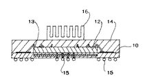
樹脂封止型の半導体装置は、図6に示すように、配線パターンを形成した配線基板10に半導体チップ12を搭載し、半導体チップ12と配線パターン間とをワイヤ13によって電気的に接続し、封止樹脂14により半導体チップ12が封止されてなる。15は外部接続用のボールバンプである。
半導体チップ12から発生した熱は、封止樹脂14表面にヒートシンク16を設けるなどして放熱を図るようにしている(例えば特許文献1参照)。
【0003】
【特許文献1】
特開平10−247702号公報
【0004】
【発明が解決しようとする課題】
しかし、上記従来の半導体装置では、半導体チップ12とヒートシンク16との間に封止樹脂14が介在していることから、放熱性が十分でないという課題がある。
【0005】
そこで本発明は上記課題を解決すべくなされたものであり、その目的とするところは、放熱性に優れる半導体装置を提供するにある。
【0006】
【課題を解決するための手段】
上記課題を解決するため、本発明に係る半導体装置は、配線基板上に半導体チップが電気的に接続して搭載され、該半導体チップが封止樹脂により封止されている半導体装置において、前記半導体チップ表面にメタライズ部が形成され、該メタライズ部に一端が接続された放熱用の金属線が複数本設けられ、該各金属線の他端が前記封止樹脂表面から露出していることを特徴としている。
【0007】
また、前記半導体チップが前記配線基板上の配線パターンにワイヤにより電気的に接続され、前記金属線が前記ワイヤのワイヤボンディングの際に前記メタライズ部に一端がボンディングされると共に他端側が外方に引き出されて所要長さに切断されることを特徴とする。
また、前記半導体チップが前記配線基板上の配線パターンにフリップチップ接続により電気的に接続され、前記金属線の一端が前記半導体チップの背面側表面に形成された前記メタライズ部に接続されていることを特徴とする。
また、前記金属線の他端側に共通の放熱板が配設されていることを特徴とする。
また、前記配線基板の前記半導体チップが搭載される面と反対側の面に外部接続用のボールバンプが形成されていることを特徴とする。
【0008】
また本発明に係る半導体装置は、配線基板上に半導体チップが電気的に接続して搭載され、該半導体チップが封止樹脂により封止されている半導体装置において、一方の面に複数本の金属線が一端側で固定された放熱板が、該一方の面側を前記配線基板側に向けて、前記金属線の他端が前記半導体チップ表面に当接するように配置された状態で、前記封止樹脂により半導体チップが封止され、かつ前記放熱板が該封止樹脂により固定されていることを特徴としている。
【0009】
また、前記放熱板の他方の面が前記封止樹脂から露出していることを特徴とする。
また、前記半導体チップが前記配線基板上の配線パターンにワイヤにより電気的に接続されていることを特徴とする。
また、前記半導体チップが前記配線基板上の配線パターンにフリップチップ接続により電気的に接続されていることを特徴とする。
また、前記配線基板の前記半導体チップが搭載される面と反対側の面に外部接続用のボールバンプが形成されていることを特徴とする。
【0010】
また本発明に係る半導体装置は、配線基板上に半導体チップが電気的に接続して搭載され、該半導体チップが封止樹脂により封止されている半導体装置において、前記封止樹脂の表面に、前記半導体チップと対応する位置に透孔が形成された放熱板が前記封止樹脂により固定され、前記半導体チップ表面にメタライズ部が形成され、該メタライズ部に一端が接続された放熱用の金属線が複数本設けられ、該各金属線の他端が前記透孔から外部に引き出されて前記放熱板の外表面に固定されていることを特徴としている。
また、前記放熱板が、支持部材を介して前記配線基板の表面から所定距離離間した位置に支持されていることを特徴とする。
【0011】
さらに本発明に係る半導体装置は、配線基板上に半導体チップが電気的に接続して搭載され、該半導体チップが封止樹脂により封止されている半導体装置において、前記半導体チップが前記配線基板上にフリップチップ接続して搭載され、前記封止樹脂の表面に、前記半導体チップと対応する位置に透孔が形成されると共に、該透孔内壁に内方に向けて突出する複数本の金属線が突設された放熱板が前記封止樹脂により固定され、前記金属線が前記半導体チップの背面に当接していることを特徴とする半導体装置。
また、前記金属線が前記放熱板と一体に形成されていることを特徴とする請求項13記載の半導体装置。
【0012】
【発明の実施の形態】
以下本発明の好適な実施の形態を添付図面に基づいて詳細に説明する。
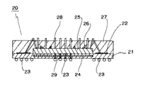
図1は半導体装置20の第1の実施の形態を示す説明図である。
21は配線基板であり、樹脂基板に配線パターン22が形成されてなる。配線基板21は公知の方法により形成できる。図示の例では樹脂基板の表面に配線パターン22が形成され、樹脂基板の下面側に引き出された端子に外部接続用のボールバンプ23が形成されたBGAタイプの配線基板21に形成されている。
【0013】
樹脂基板上に半導体チップ25が搭載され、半導体チップ25と配線パターン22とがワイヤ26により電気的に接続されている。
半導体チップ25は封止樹脂27により封止されている。
以上は従来の半導体装置と同様の構造である。
本実施の形態では、半導体チップ25と配線パターン22との間がワイヤボンディングされる際、同時にボンダーにより金属線28の一端が半導体チップ25の表面にボンディングされ、他端側が外方に引き出されて所要長さに切断される。
金属線28の他端側は封止樹脂27の外部に露出される。
【0014】
半導体チップ25の表面に金属線28がボンディングできるように、ワイヤ26がボンディングされる部位と同様に、半導体チップ25表面に金属部(メタライズ部、図示せず)を半導体チップ25のパターン形成の際に同時に作りこんでおくようにするとよい。
金属線28はワイヤ26と同一の材質のものでも違うものでもよい。太さも任意であるが、放熱性を高めるためにできるだけ太いものを用いるのが好適である。
また金属線28の本数も、半導体チップ25の空きスペースを有効に用いてできるだけ多く設けるようにするとよい。
【0015】
上記のように、半導体チップ25に一端が固定された金属線28が外方に引き出され、他端が封止樹脂27の外部に露出されていることから、特に半導体チップ25表面で発生した熱が金属線28を伝って外部に放熱されるので放熱効果を高めることができる。
また、ワイヤ26のうち外部に露出させても構わない、例えば接地線(グランド線)などを、一部を図示のように封止樹脂27から外部に露出させることによって一層放熱効果を高めることができる。
【0016】
また、上記では半導体チップ25と配線パターン22との間をワイヤ26により接続したが、場合によっては半導体チップ25をフリップチップ接続により配線基板21に搭載してもよい。この場合は半導体チップ25の背面側全面を利用できるので、より多くの金属線28を設けることができ、放熱効果を高められる。
【0017】
なお、図示の例では、配線基板21は多層に形成され、内部に金属箔等からなるサーマルプレーン24が配設され、このサーマルプレーン24、半導体チップ25、放熱用のボールバンプ23が、サーマルビア29により接続されて、半導体チップ25で発生した熱がサーマルプレーン24、サーマルビア29を通じて放熱されるようになっている。サーマルプレーン24は、接地プレーンもしくは電源プレーンを兼用することもできる。このサーマルプレーン24は必ずしも設けなくともよい。
【0018】
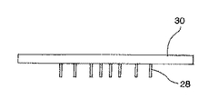
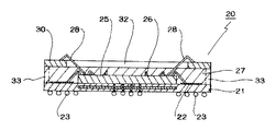
図2は、図1に示すものにおいて、複数の金属線28の他端側に共通の放熱板30を配設した第2の実施の形態を示す。
放熱板30は、金属線28の他端側に固定しても、単に載置したものであってもよい。放熱板30は封止樹脂27に固着されている。
放熱板30は図示のように少なくとも片面を封止樹脂27から露出させるのが好ましいが、場合によっては封止樹脂27中に埋没させてもよい。
【0019】
放熱板30は金属製の他、窒化アルミニウム等の放熱性の良好な材料のものを用いることができる。
また、放熱板30にヒートシンク31を取りつけてもよい。
また、サーマルプレーン24から配線基板21上に引き出したパッド(図示せず)上に金属線28を立設し、この金属線28を放熱板30に当接させてもよい。
【0020】
図3は第3の実施の形態を示す。
本実施の形態では、図3に示すように、あらかじめ放熱板30の側に複数本の金属線28を一端側で溶接等によって固定したものを用意する。そしてこの放熱板30を、該一方の面側を配線基板21側に向けて、金属線28の他端が半導体チップ25表面に当接するように配置し、この状態で金型内に組み込み、モールドして、封止樹脂27により半導体チップ25が封止され、かつ放熱板30が封止樹脂27により固定された、図2に示すのと同等な半導体装置20に形成するのである(図面的には図2と同一になるので図示を省略する。
【0021】
本実施の形態でも同様に放熱性に優れる半導体装置20を提供できる。
金属線28をあらかじめ放熱板30に固定するものであるため、容易に放熱板30を形成できる。
なお、本実施の形態においても半導体チップ25はワイヤにより電気的に接続しても、フリップチップ接続により電気的に接続しても、いずれでもよい。
【0022】
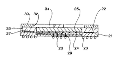
図4は第4の実施の形態を示す。
上記実施の形態と同一の部材は同一符号を付している。
本実施の形態では、封止樹脂27の表面に、半導体チップ25と対応する位置に透孔32が形成された放熱板30が封止樹脂27により固定され、半導体チップ25表面にメタライズ部(図示せず)が形成され、該メタライズ部に一端が接続された放熱用の金属線28が複数本設けられ、該各金属線28の他端が透孔32から外部に引き出されて放熱板30の外表面に固定されてなる。
なお、放熱板30は、支持部材33を介して配線基板21の表面から所定距離離間した位置に支持されている。放熱板30と配線基板21との間の間隙に封止樹脂27が充填される。
本実施の形態においても、金属線28および放熱板30を介して半導体チップ25から発生した熱が直接外部に放出されるので、放熱効果に優れる。
【0023】
図5は第5の実施の形態を示す。
上記実施の形態と同一の部材は同一符号を付している。
本実施の形態では、図4に示す実施の形態のものにおいて、半導体チップ25が配線基板21上にフリップチップ接続して搭載されている。放熱板30の、半導体チップ25と対応する位置に透孔32が形成されていて、放熱板30は封止樹脂27により固定されている。透孔32内壁には内方に向けて複数本の金属線34が突設され、この金属線34が半導体チップ25の背面上に当接している。
封止樹脂27は金属線34間に進入し、また半導体チップ25上を覆っている。
33は支持部材である。
本実施の形態においても、金属線34および放熱板30を介して半導体チップ25から発生した熱が直接外部に放出されるので、放熱効果に優れる。
金属線34は、金属板を打ち抜き加工等することによって、放熱板30と一体的に形成でき、好適である。
【0024】
【発明の効果】
以上のように、本発明によれば、半導体チップに直接接続される金属線を介して、半導体チップで発生した熱を外部に直接放出できるので放熱効果に優れる。
【図面の簡単な説明】
【図1】第1の実施の形態を示す断面説明図である。
【図2】第2の実施の形態を示す断面説明図である。
【図3】第3の実施の形態を示す断面説明図である。
【図4】第4の実施の形態を示す断面説明図である。
【図5】第5の実施の形態を示す断面説明図である。
【図6】従来の半導体装置の一例を示す断面説明図である。
【符号の説明】
20 半導体装置
21 配線基板
22 配線パターン
23 ボールバンプ
25 半導体チップ
26 ワイヤ
27 封止樹脂
28 金属線
30 放熱板
32 透孔
33 支持部[0001]
TECHNICAL FIELD OF THE INVENTION
The present invention relates to a semiconductor device having excellent heat dissipation.
[0002]
[Prior art]
As shown in FIG. 6, the resin-encapsulated semiconductor device mounts a
The heat generated from the
[0003]
[Patent Document 1]
JP 10-247702 A
[Problems to be solved by the invention]
However, in the above-described conventional semiconductor device, there is a problem that heat dissipation is not sufficient because the
[0005]
Therefore, the present invention has been made to solve the above problems, and an object of the present invention is to provide a semiconductor device having excellent heat dissipation.
[0006]
[Means for Solving the Problems]
In order to solve the above problems, a semiconductor device according to the present invention is a semiconductor device, wherein a semiconductor chip is electrically connected and mounted on a wiring board, and the semiconductor chip is sealed with a sealing resin. A metallized portion is formed on the chip surface, a plurality of heat dissipating metal wires having one end connected to the metallized portion are provided, and the other end of each metal wire is exposed from the sealing resin surface. And
[0007]
In addition, the semiconductor chip is electrically connected to a wiring pattern on the wiring board by a wire, and the metal wire is bonded at one end to the metallized portion during wire bonding of the wire, and the other end is outward. It is drawn out and cut to a required length.
Further, the semiconductor chip is electrically connected to a wiring pattern on the wiring board by flip-chip connection, and one end of the metal wire is connected to the metallized portion formed on the back surface of the semiconductor chip. It is characterized by.
Further, a common radiator plate is provided on the other end side of the metal wire.
Further, a ball bump for external connection is formed on a surface of the wiring substrate opposite to a surface on which the semiconductor chip is mounted.
[0008]
Further, in the semiconductor device according to the present invention, in a semiconductor device in which a semiconductor chip is electrically connected and mounted on a wiring board and the semiconductor chip is sealed with a sealing resin, a plurality of metal chips may be provided on one surface. In a state in which a heat sink to which a wire is fixed at one end is disposed such that the one surface side faces the wiring board and the other end of the metal wire is in contact with the surface of the semiconductor chip, the sealing is performed. The semiconductor chip is sealed with a sealing resin, and the heat sink is fixed with the sealing resin.
[0009]
Further, the other surface of the heat sink is exposed from the sealing resin.
Further, the semiconductor chip is electrically connected to a wiring pattern on the wiring board by a wire.
Further, the semiconductor chip is electrically connected to a wiring pattern on the wiring board by flip-chip connection.
Further, a ball bump for external connection is formed on a surface of the wiring substrate opposite to a surface on which the semiconductor chip is mounted.
[0010]
Further, the semiconductor device according to the present invention is a semiconductor device in which a semiconductor chip is electrically connected and mounted on a wiring board, and the semiconductor chip is sealed with a sealing resin. A heat radiating plate having a through hole formed at a position corresponding to the semiconductor chip is fixed by the sealing resin, a metallized portion is formed on the surface of the semiconductor chip, and a metal wire for heat radiating having one end connected to the metallized portion Are provided, and the other end of each of the metal wires is drawn out of the through hole to the outside and is fixed to the outer surface of the heat sink.
Further, the heat radiating plate is supported at a position separated from the surface of the wiring board by a predetermined distance via a supporting member.
[0011]
Further, in the semiconductor device according to the present invention, the semiconductor chip is electrically connected and mounted on a wiring board, and the semiconductor chip is sealed with a sealing resin. A plurality of metal wires which are mounted on the surface of the sealing resin at a position corresponding to the semiconductor chip and which project inwardly from the inner wall of the through hole. A semiconductor device, wherein a heat radiating plate having a projection is fixed by the sealing resin, and the metal wire is in contact with a back surface of the semiconductor chip.
14. The semiconductor device according to
[0012]
BEST MODE FOR CARRYING OUT THE INVENTION
Hereinafter, preferred embodiments of the present invention will be described in detail with reference to the accompanying drawings.
FIG. 1 is an explanatory diagram showing a first embodiment of the
[0013]
A
The
The above is the same structure as the conventional semiconductor device.
In the present embodiment, when wire bonding is performed between the
The other end of the
[0014]
A metal portion (metallized portion, not shown) is formed on the surface of the
The
Also, the number of the
[0015]
As described above, since the
Further, the heat radiation effect may be further enhanced by exposing a part of the ground wire (ground line) which may be exposed to the outside of the
[0016]
In the above description, the
[0017]
In the illustrated example, the
[0018]
FIG. 2 shows a second embodiment in which a
The
It is preferable that at least one surface of the
[0019]
The
Further, the heat sink 31 may be attached to the
Alternatively, the
[0020]
FIG. 3 shows a third embodiment.
In the present embodiment, as shown in FIG. 3, one in which a plurality of
[0021]
Also in the present embodiment, it is possible to provide the
Since the
In this embodiment, the
[0022]
FIG. 4 shows a fourth embodiment.
The same members as those in the above embodiment are denoted by the same reference numerals.
In the present embodiment, a
Note that the
Also in the present embodiment, since the heat generated from the
[0023]
FIG. 5 shows a fifth embodiment.
The same members as those in the above embodiment are denoted by the same reference numerals.
In the present embodiment, in the embodiment shown in FIG. 4, a
The sealing
33 is a support member.
Also in the present embodiment, since the heat generated from the
The
[0024]
【The invention's effect】
As described above, according to the present invention, heat generated in the semiconductor chip can be directly radiated to the outside via the metal wire directly connected to the semiconductor chip, so that the heat radiation effect is excellent.
[Brief description of the drawings]
FIG. 1 is an explanatory cross-sectional view showing a first embodiment.
FIG. 2 is an explanatory sectional view showing a second embodiment.
FIG. 3 is an explanatory cross-sectional view showing a third embodiment.
FIG. 4 is an explanatory sectional view showing a fourth embodiment.
FIG. 5 is an explanatory sectional view showing a fifth embodiment.
FIG. 6 is an explanatory sectional view showing an example of a conventional semiconductor device.
[Explanation of symbols]
Claims (14)
前記半導体チップ表面にメタライズ部が形成され、該メタライズ部に一端が接続された放熱用の金属線が複数本設けられ、該各金属線の他端が前記封止樹脂表面から露出していることを特徴とする半導体装置。In a semiconductor device in which a semiconductor chip is electrically connected and mounted on a wiring board, and the semiconductor chip is sealed with a sealing resin,
A metallized portion is formed on the surface of the semiconductor chip, a plurality of heat-dissipating metal wires having one end connected to the metallized portion are provided, and the other end of each metal wire is exposed from the sealing resin surface. A semiconductor device characterized by the above-mentioned.
一方の面に複数本の金属線が一端側で固定された放熱板が、該一方の面側を前記配線基板側に向けて、前記金属線の他端が前記半導体チップ表面に当接するように配置された状態で、前記封止樹脂により半導体チップが封止され、かつ前記放熱板が該封止樹脂により固定されていることを特徴とする半導体装置。In a semiconductor device in which a semiconductor chip is electrically connected and mounted on a wiring board, and the semiconductor chip is sealed with a sealing resin,
A radiator plate having a plurality of metal wires fixed to one surface at one end, with the one surface facing the wiring board, and the other end of the metal wire abutting the semiconductor chip surface. A semiconductor device, wherein a semiconductor chip is sealed with the sealing resin and the radiator plate is fixed with the sealing resin in the arranged state.
前記封止樹脂の表面に、前記半導体チップと対応する位置に透孔が形成された放熱板が前記封止樹脂により固定され、前記半導体チップ表面にメタライズ部が形成され、該メタライズ部に一端が接続された放熱用の金属線が複数本設けられ、該各金属線の他端が前記透孔から外部に引き出されて前記放熱板の外表面に固定されていることを特徴とする半導体装置。In a semiconductor device in which a semiconductor chip is electrically connected and mounted on a wiring board, and the semiconductor chip is sealed with a sealing resin,
On the surface of the sealing resin, a heat sink having a through hole formed at a position corresponding to the semiconductor chip is fixed by the sealing resin, a metallized portion is formed on the surface of the semiconductor chip, and one end is formed on the metalized portion. A semiconductor device, wherein a plurality of connected metal wires for heat dissipation are provided, and the other end of each metal wire is drawn out of the through hole to the outside and fixed to the outer surface of the heat sink.
前記半導体チップが前記配線基板上にフリップチップ接続して搭載され、
前記封止樹脂の表面に、前記半導体チップと対応する位置に透孔が形成されると共に、該透孔内壁に内方に向けて突出する複数本の金属線が突設された放熱板が前記封止樹脂により固定され、
前記金属線が前記半導体チップの背面に当接していることを特徴とする半導体装置。In a semiconductor device in which a semiconductor chip is electrically connected and mounted on a wiring board, and the semiconductor chip is sealed with a sealing resin,
The semiconductor chip is mounted on the wiring board by flip-chip connection,
On the surface of the sealing resin, a through hole is formed at a position corresponding to the semiconductor chip, and a heat radiating plate on which a plurality of metal wires projecting inward from the inner wall of the through hole is provided. Fixed with sealing resin,
The semiconductor device, wherein the metal wire is in contact with a back surface of the semiconductor chip.
Priority Applications (1)
| Application Number | Priority Date | Filing Date | Title |
|---|---|---|---|
| JP2002365679A JP2004200316A (en) | 2002-12-17 | 2002-12-17 | Semiconductor device |
Applications Claiming Priority (1)
| Application Number | Priority Date | Filing Date | Title |
|---|---|---|---|
| JP2002365679A JP2004200316A (en) | 2002-12-17 | 2002-12-17 | Semiconductor device |
Publications (1)
| Publication Number | Publication Date |
|---|---|
| JP2004200316A true JP2004200316A (en) | 2004-07-15 |
Family
ID=32763164
Family Applications (1)
| Application Number | Title | Priority Date | Filing Date |
|---|---|---|---|
| JP2002365679A Pending JP2004200316A (en) | 2002-12-17 | 2002-12-17 | Semiconductor device |
Country Status (1)
| Country | Link |
|---|---|
| JP (1) | JP2004200316A (en) |
Cited By (31)
| Publication number | Priority date | Publication date | Assignee | Title |
|---|---|---|---|---|
| WO2007016088A2 (en) | 2005-07-29 | 2007-02-08 | Freescale Semiconductor | Packaged integrated circuit with enhanced thermal dissipation |
| KR101463988B1 (en) * | 2006-09-29 | 2014-11-20 | 티디케이가부시기가이샤 | Semiconductor embedded substrate and method for manufacturing the same |
| EP2036123B1 (en) * | 2006-06-16 | 2015-09-23 | International Business Machines Corporation | Cooled electronic assembly employing a thermally conductive composite interface material and fabrication method thereof |
| WO2016094134A1 (en) * | 2014-12-11 | 2016-06-16 | Invensas Corporation | Microelectronic device with integrated circuit die and thermal wires enclosed in molding material |
| WO2016150934A1 (en) * | 2015-03-24 | 2016-09-29 | 3D Plus | Electronic chip device with improved thermal resistance and associated manufacturing process |
| US9761554B2 (en) | 2015-05-07 | 2017-09-12 | Invensas Corporation | Ball bonding metal wire bond wires to metal pads |
| US9812402B2 (en) | 2015-10-12 | 2017-11-07 | Invensas Corporation | Wire bond wires for interference shielding |
| US9842745B2 (en) | 2012-02-17 | 2017-12-12 | Invensas Corporation | Heat spreading substrate with embedded interconnects |
| US9852969B2 (en) | 2013-11-22 | 2017-12-26 | Invensas Corporation | Die stacks with one or more bond via arrays of wire bond wires and with one or more arrays of bump interconnects |
| US9888579B2 (en) | 2015-03-05 | 2018-02-06 | Invensas Corporation | Pressing of wire bond wire tips to provide bent-over tips |
| US9911718B2 (en) | 2015-11-17 | 2018-03-06 | Invensas Corporation | ‘RDL-First’ packaged microelectronic device for a package-on-package device |
| US9935075B2 (en) | 2016-07-29 | 2018-04-03 | Invensas Corporation | Wire bonding method and apparatus for electromagnetic interference shielding |
| US9953914B2 (en) | 2012-05-22 | 2018-04-24 | Invensas Corporation | Substrate-less stackable package with wire-bond interconnect |
| US9984992B2 (en) | 2015-12-30 | 2018-05-29 | Invensas Corporation | Embedded wire bond wires for vertical integration with separate surface mount and wire bond mounting surfaces |
| US10008477B2 (en) | 2013-09-16 | 2018-06-26 | Invensas Corporation | Microelectronic element with bond elements to encapsulation surface |
| US10008469B2 (en) | 2015-04-30 | 2018-06-26 | Invensas Corporation | Wafer-level packaging using wire bond wires in place of a redistribution layer |
| US10026717B2 (en) | 2013-11-22 | 2018-07-17 | Invensas Corporation | Multiple bond via arrays of different wire heights on a same substrate |
| US10062661B2 (en) | 2011-05-03 | 2018-08-28 | Tessera, Inc. | Package-on-package assembly with wire bonds to encapsulation surface |
| US10128216B2 (en) | 2010-07-19 | 2018-11-13 | Tessera, Inc. | Stackable molded microelectronic packages |
| US10181457B2 (en) | 2015-10-26 | 2019-01-15 | Invensas Corporation | Microelectronic package for wafer-level chip scale packaging with fan-out |
| US10297582B2 (en) | 2012-08-03 | 2019-05-21 | Invensas Corporation | BVA interposer |
| US10299368B2 (en) | 2016-12-21 | 2019-05-21 | Invensas Corporation | Surface integrated waveguides and circuit structures therefor |
| US10332854B2 (en) | 2015-10-23 | 2019-06-25 | Invensas Corporation | Anchoring structure of fine pitch bva |
| US10381326B2 (en) | 2014-05-28 | 2019-08-13 | Invensas Corporation | Structure and method for integrated circuits packaging with increased density |
| US10460958B2 (en) | 2013-08-07 | 2019-10-29 | Invensas Corporation | Method of manufacturing embedded packaging with preformed vias |
| US10490528B2 (en) | 2015-10-12 | 2019-11-26 | Invensas Corporation | Embedded wire bond wires |
| US10529636B2 (en) | 2014-01-17 | 2020-01-07 | Invensas Corporation | Fine pitch BVA using reconstituted wafer with area array accessible for testing |
| US10756049B2 (en) | 2011-10-17 | 2020-08-25 | Invensas Corporation | Package-on-package assembly with wire bond vias |
| EP3926679A1 (en) * | 2020-06-17 | 2021-12-22 | Infineon Technologies AG | Power semiconductor module arrangement comprising a temperature sensor |
| US12315776B2 (en) | 2021-11-08 | 2025-05-27 | Analog Devices, Inc. | Integrated device package with an integrated heat sink |
| US12494453B2 (en) | 2011-05-03 | 2025-12-09 | Adeia Semiconductor Solutions Llc | Package-on-package assembly with wire bonds to encapsulation surface |
-
2002
- 2002-12-17 JP JP2002365679A patent/JP2004200316A/en active Pending
Cited By (59)
| Publication number | Priority date | Publication date | Assignee | Title |
|---|---|---|---|---|
| JP2009503865A (en) * | 2005-07-29 | 2009-01-29 | フリースケール セミコンダクター インコーポレイテッド | Packaged integrated circuits with enhanced heat dissipation |
| EP1913633B1 (en) * | 2005-07-29 | 2018-11-14 | NXP USA, Inc. | Packaged integrated circuit with enhanced thermal dissipation |
| WO2007016088A2 (en) | 2005-07-29 | 2007-02-08 | Freescale Semiconductor | Packaged integrated circuit with enhanced thermal dissipation |
| EP2036123B1 (en) * | 2006-06-16 | 2015-09-23 | International Business Machines Corporation | Cooled electronic assembly employing a thermally conductive composite interface material and fabrication method thereof |
| EP1906436B1 (en) * | 2006-09-29 | 2019-06-05 | TDK Corporation | Semiconductor-embedded substrate and manufacturing method thereof |
| KR101463988B1 (en) * | 2006-09-29 | 2014-11-20 | 티디케이가부시기가이샤 | Semiconductor embedded substrate and method for manufacturing the same |
| US10128216B2 (en) | 2010-07-19 | 2018-11-13 | Tessera, Inc. | Stackable molded microelectronic packages |
| US12494453B2 (en) | 2011-05-03 | 2025-12-09 | Adeia Semiconductor Solutions Llc | Package-on-package assembly with wire bonds to encapsulation surface |
| US10062661B2 (en) | 2011-05-03 | 2018-08-28 | Tessera, Inc. | Package-on-package assembly with wire bonds to encapsulation surface |
| US11424211B2 (en) | 2011-05-03 | 2022-08-23 | Tessera Llc | Package-on-package assembly with wire bonds to encapsulation surface |
| US10593643B2 (en) | 2011-05-03 | 2020-03-17 | Tessera, Inc. | Package-on-package assembly with wire bonds to encapsulation surface |
| US11735563B2 (en) | 2011-10-17 | 2023-08-22 | Invensas Llc | Package-on-package assembly with wire bond vias |
| US10756049B2 (en) | 2011-10-17 | 2020-08-25 | Invensas Corporation | Package-on-package assembly with wire bond vias |
| US11189595B2 (en) | 2011-10-17 | 2021-11-30 | Invensas Corporation | Package-on-package assembly with wire bond vias |
| US9842745B2 (en) | 2012-02-17 | 2017-12-12 | Invensas Corporation | Heat spreading substrate with embedded interconnects |
| US10510659B2 (en) | 2012-05-22 | 2019-12-17 | Invensas Corporation | Substrate-less stackable package with wire-bond interconnect |
| US10170412B2 (en) | 2012-05-22 | 2019-01-01 | Invensas Corporation | Substrate-less stackable package with wire-bond interconnect |
| US9953914B2 (en) | 2012-05-22 | 2018-04-24 | Invensas Corporation | Substrate-less stackable package with wire-bond interconnect |
| US10297582B2 (en) | 2012-08-03 | 2019-05-21 | Invensas Corporation | BVA interposer |
| US10460958B2 (en) | 2013-08-07 | 2019-10-29 | Invensas Corporation | Method of manufacturing embedded packaging with preformed vias |
| US10008477B2 (en) | 2013-09-16 | 2018-06-26 | Invensas Corporation | Microelectronic element with bond elements to encapsulation surface |
| US10629567B2 (en) | 2013-11-22 | 2020-04-21 | Invensas Corporation | Multiple plated via arrays of different wire heights on same substrate |
| US10026717B2 (en) | 2013-11-22 | 2018-07-17 | Invensas Corporation | Multiple bond via arrays of different wire heights on a same substrate |
| USRE49987E1 (en) | 2013-11-22 | 2024-05-28 | Invensas Llc | Multiple plated via arrays of different wire heights on a same substrate |
| US9852969B2 (en) | 2013-11-22 | 2017-12-26 | Invensas Corporation | Die stacks with one or more bond via arrays of wire bond wires and with one or more arrays of bump interconnects |
| US10290613B2 (en) | 2013-11-22 | 2019-05-14 | Invensas Corporation | Multiple bond via arrays of different wire heights on a same substrate |
| US11404338B2 (en) | 2014-01-17 | 2022-08-02 | Invensas Corporation | Fine pitch bva using reconstituted wafer with area array accessible for testing |
| US11990382B2 (en) | 2014-01-17 | 2024-05-21 | Adeia Semiconductor Technologies Llc | Fine pitch BVA using reconstituted wafer with area array accessible for testing |
| US10529636B2 (en) | 2014-01-17 | 2020-01-07 | Invensas Corporation | Fine pitch BVA using reconstituted wafer with area array accessible for testing |
| US10381326B2 (en) | 2014-05-28 | 2019-08-13 | Invensas Corporation | Structure and method for integrated circuits packaging with increased density |
| WO2016094134A1 (en) * | 2014-12-11 | 2016-06-16 | Invensas Corporation | Microelectronic device with integrated circuit die and thermal wires enclosed in molding material |
| US9735084B2 (en) | 2014-12-11 | 2017-08-15 | Invensas Corporation | Bond via array for thermal conductivity |
| US10806036B2 (en) | 2015-03-05 | 2020-10-13 | Invensas Corporation | Pressing of wire bond wire tips to provide bent-over tips |
| US9888579B2 (en) | 2015-03-05 | 2018-02-06 | Invensas Corporation | Pressing of wire bond wire tips to provide bent-over tips |
| KR102524167B1 (en) | 2015-03-24 | 2023-04-20 | 3디 플러스 | Electronic chip device with improved thermal resistance and associated manufacturing process |
| FR3034253A1 (en) * | 2015-03-24 | 2016-09-30 | 3D Plus | ELECTRONIC CHIP DEVICE WITH IMPROVED THERMAL RESISTANCE AND METHOD OF MANUFACTURING THE SAME |
| CN108496248A (en) * | 2015-03-24 | 2018-09-04 | 3D加公司 | Electronic chip device and related manufacturing process with improved thermal resistance |
| CN108496248B (en) * | 2015-03-24 | 2021-11-26 | 3D加公司 | Electronic chip device with improved thermal resistance and related manufacturing process |
| JP2018509771A (en) * | 2015-03-24 | 2018-04-05 | スリーディー プラス | Electronic chip devices with improved thermal resistance and associated manufacturing processes |
| WO2016150934A1 (en) * | 2015-03-24 | 2016-09-29 | 3D Plus | Electronic chip device with improved thermal resistance and associated manufacturing process |
| KR20170129889A (en) * | 2015-03-24 | 2017-11-27 | 3디 플러스 | Electronic chip device with improved thermal resistance and associated manufacturing process |
| US10008469B2 (en) | 2015-04-30 | 2018-06-26 | Invensas Corporation | Wafer-level packaging using wire bond wires in place of a redistribution layer |
| US9761554B2 (en) | 2015-05-07 | 2017-09-12 | Invensas Corporation | Ball bonding metal wire bond wires to metal pads |
| US10490528B2 (en) | 2015-10-12 | 2019-11-26 | Invensas Corporation | Embedded wire bond wires |
| US9812402B2 (en) | 2015-10-12 | 2017-11-07 | Invensas Corporation | Wire bond wires for interference shielding |
| US10559537B2 (en) | 2015-10-12 | 2020-02-11 | Invensas Corporation | Wire bond wires for interference shielding |
| US10115678B2 (en) | 2015-10-12 | 2018-10-30 | Invensas Corporation | Wire bond wires for interference shielding |
| US11462483B2 (en) | 2015-10-12 | 2022-10-04 | Invensas Llc | Wire bond wires for interference shielding |
| US10332854B2 (en) | 2015-10-23 | 2019-06-25 | Invensas Corporation | Anchoring structure of fine pitch bva |
| US10181457B2 (en) | 2015-10-26 | 2019-01-15 | Invensas Corporation | Microelectronic package for wafer-level chip scale packaging with fan-out |
| US9911718B2 (en) | 2015-11-17 | 2018-03-06 | Invensas Corporation | ‘RDL-First’ packaged microelectronic device for a package-on-package device |
| US10043779B2 (en) | 2015-11-17 | 2018-08-07 | Invensas Corporation | Packaged microelectronic device for a package-on-package device |
| US9984992B2 (en) | 2015-12-30 | 2018-05-29 | Invensas Corporation | Embedded wire bond wires for vertical integration with separate surface mount and wire bond mounting surfaces |
| US10325877B2 (en) | 2015-12-30 | 2019-06-18 | Invensas Corporation | Embedded wire bond wires for vertical integration with separate surface mount and wire bond mounting surfaces |
| US9935075B2 (en) | 2016-07-29 | 2018-04-03 | Invensas Corporation | Wire bonding method and apparatus for electromagnetic interference shielding |
| US10658302B2 (en) | 2016-07-29 | 2020-05-19 | Invensas Corporation | Wire bonding method and apparatus for electromagnetic interference shielding |
| US10299368B2 (en) | 2016-12-21 | 2019-05-21 | Invensas Corporation | Surface integrated waveguides and circuit structures therefor |
| EP3926679A1 (en) * | 2020-06-17 | 2021-12-22 | Infineon Technologies AG | Power semiconductor module arrangement comprising a temperature sensor |
| US12315776B2 (en) | 2021-11-08 | 2025-05-27 | Analog Devices, Inc. | Integrated device package with an integrated heat sink |
Similar Documents
| Publication | Publication Date | Title |
|---|---|---|
| JP2004200316A (en) | Semiconductor device | |
| JP4493121B2 (en) | Semiconductor device and semiconductor chip packaging method | |
| JP3854054B2 (en) | Semiconductor device | |
| US20050012203A1 (en) | Enhanced die-down ball grid array and method for making the same | |
| KR102172689B1 (en) | Semiconductor package and method of fabricating the same | |
| JPH08222690A (en) | Semiconductor module for microprocessor | |
| JP2005217405A (en) | Heat emission type semiconductor package and manufacturing method thereof | |
| US6643136B2 (en) | Multi-chip package with embedded cooling element | |
| JP2004214548A (en) | Component built-in board type module, board on which it is mounted, method of manufacturing component built-in board type module, and method of manufacturing board mounted with component built-in board type module | |
| JP3650689B2 (en) | Semiconductor device | |
| US20050121759A1 (en) | Semiconductor package with a chip on a support plate | |
| JP2006120996A (en) | Circuit module | |
| JP3922809B2 (en) | Semiconductor device | |
| JP2000252419A (en) | 3D module structure | |
| JPH04207061A (en) | Semiconductor device | |
| TWI269414B (en) | Package substrate with improved structure for thermal dissipation and electronic device using the same | |
| JPH08264688A (en) | Ceramic package for semiconductor | |
| JP3378174B2 (en) | Heat dissipation structure of high heating element | |
| JP3570672B2 (en) | Semiconductor device | |
| JP2003273297A (en) | Electronic equipment | |
| CN118039583A (en) | Packaging module | |
| JP2008085002A (en) | Semiconductor device and manufacturing method thereof | |
| JP2003023126A (en) | Semiconductor device | |
| CN112312678A (en) | Structure and method of non-packaged chip direct-buried printed circuit board and chip packaging structure | |
| JPH0878616A (en) | Multi-chip module |