JP2004200331A - Optical communication device - Google Patents
Optical communication device Download PDFInfo
- Publication number
- JP2004200331A JP2004200331A JP2002365985A JP2002365985A JP2004200331A JP 2004200331 A JP2004200331 A JP 2004200331A JP 2002365985 A JP2002365985 A JP 2002365985A JP 2002365985 A JP2002365985 A JP 2002365985A JP 2004200331 A JP2004200331 A JP 2004200331A
- Authority
- JP
- Japan
- Prior art keywords
- lead
- optical communication
- package case
- communication device
- package
- Prior art date
- Legal status (The legal status is an assumption and is not a legal conclusion. Google has not performed a legal analysis and makes no representation as to the accuracy of the status listed.)
- Pending
Links
Images


Landscapes
- Semiconductor Lasers (AREA)
Abstract
Description
【0001】
【発明の属する技術分野】
本発明は光通信装置に関し、特に、光通信における送信用や受信用の光通信モジュールの製造技術に適用して有効な技術に関する。
【0002】
【従来の技術】
情報処理装置用光源や光通信装置用光源として、半導体レーザ(レーザダイオード)が用いられている。光通信においては、送信用光通信モジュールや受信用光通信モジュール等の光電子装置が使用されている。例えば、特開平10-307235号公報には送信用の半導体レーザモジュール及びその製造技術が開示されている。この文献には、パッケージケースの内底面に固定したシリコン基板の主面にレーザダイオード,フォトダイオード及び光ファイバを搭載する(所謂パッシブアライメント実装)とともに、前記パッケージケースをキャップで封止した半導体レーザモジュールが記載されている。パッケージケースはプラスチックをモールディング(成形)し、リード端子付きパッド部及びパッケージケース側壁の光ファイバ設置溝と光ファイバ被覆部設置溝を一体に形成した形状になっている。
【0003】
また、同種の構成として、パッケージが気密封止構造となるセラミックパッケージ構造の光通信モジュールがあるが、この種のセラミックパッケージ構造の光通信モジュールとしては、例えば、Lucent Technologies 社、microelectronicsgroup発行、データシートDSO1-020OPTO(Replaces DS99-023LWP)、12月号、2000年、P1〜P8に記載されているようなレーザモジュールが知られている。
【0004】
【発明が解決しようとする課題】
インターネットのデータ量(トラヒック)、特に米国の幹線部分に流れるトラヒックは、驚異的なペースで増え続けている。大都市間、都市内を結ぶ高速・長距離用(例えば10Gbps,80km)伝送装置の開発が急ピッチで進められている。一方、それらの伝送装置に接続される局内インターフェースやLANなど、2km以下の短い距離を結ぶ伝送装置の高速化も求められている。
【0005】
光通信装置が広く普及するためには、その低コスト化が課題であり、もはや10Gbpsクラスの高速伝送装置も例外では無くなってきている。リードフレームを用いてトランスファモールディングしてプラスチック製のパッケージケースを製造する方法は、光通信装置のコスト低減に有効である。
【0006】
そこで、本発明者は、プラスチック製のパッケージケースを使用した光通信装置について分析検討した。この結果、以下の事実を確認した。
【0007】
従来技術ではリードやワイヤのインダクタンスが大きく、高速伝送には必ずしも適していないことが判明した。即ち、パッケージケースに組み込まれるリードは、パッケージケース内においてはパッケージケースの底に沿って延在してパッケージケースの外側に突出し、パッケージケース外においては階段状に屈曲して延在して先端が表面実装に適した実装部を有する構造になる。この結果、リードが長くなり、リードのインダクタンスが大きくなる。
【0008】
また、リード及びリードベースは一枚の平坦な金属板をパターニングして形成される。リードベース上には支持基板が固定され、さらに支持基板上に半導体レーザ素子や半導体レーザ素子に接続される抵抗が固定される。また、この抵抗の一方の電極はワイヤを介してリードに接続される。従って、ワイヤが接続される抵抗の電極面、即ち抵抗のワイヤ接続面は、リードのワイヤ接続面よりも支持基板及び半導体レーザ素子の厚さ分高くなる。この結果、高さの異なる二点間を接続するワイヤの長さは、高さが違う分長くなり、ワイヤのインダクタンスが大きくなる。
【0009】
本発明の目的は高周波特性が優れた光通信装置を提供することにある。
【0010】
本発明の他の目的は伝搬損失が小さい光通信装置を提供することにある。
【0011】
本発明の他の目的はインピーダンス整合したインダクタンス値が低い光通信装置を提供することにある。
【0012】
本発明の他の目的は低コスト化が可能な光通信装置を提供することにある。
【0013】
本発明の前記ならびにそのほかの目的と新規な特徴は、本明細書の記述および添付図面からあきらかになるであろう。
【0014】
【課題を解決するための手段】
本願において開示される発明のうち代表的なものの概要を簡単に説明すれば、下記のとおりである。
【0015】
(1)プラスチックからなり上面に開口部を有するパッケージケースと、
前記パッケージケースの上面を塞ぐキャップと、
前記パッケージケースの内外に亘って延在し、外部は電極端子となる複数の金属からなるリードと、
前記パッケージケースの内底に配置され、前記リードの少なくとも1乃至複数と一体的に形成されたリードベースと、
前記リードベース上に固定されかつ上面に所定パターンの導体層を有する支持基板と、
前記支持基板上に固定される一乃至複数の光素子と、
前記パッケージケースの内外に亘って延在するとともに、内端が前記一つの光素子(半導体レーザ素子)に対峙して前記半導体レーザ素子との間で光の授受を行うように前記支持基板上に固定される光ファイバと、
前記パッケージケース内の前記リードベースを含むリードに固定される1乃至複数の電子部品と、
前記光素子の電極,前記電子部品の電極,前記支持基板の導体層並びに前記リードのそれぞれを必要に応じて電気的に接続する導電性のワイヤとを有する光通信装置であって、
前記リードのうち高周波信号入力部を構成する信号リードはその両側に接地電極となるグランドリードが所定間隔離れるように配置され、前記信号リード及び前記両側のグランドリード並びに前記信号リードと前記グランドリードを支持する前記パッケージケース部分によってインピーダンス整合されたコプレーナ伝送線路が構成されていることを特徴とする。
【0016】
前記リードは前記開口部に位置し前記ワイヤが接続される平坦面部と、この平坦面部に連なる傾斜面部と、この傾斜面部に連なり先端部分が前記パッケージケースから突出する実装部とからなっている。前記光素子(半導体レーザ素子)の高周波信号入力部となる前記リードは前記傾斜面部が他のリードよりも長くなり、前記平坦面部の高さが前記リードベース面よりも高くなり、前記平坦面部のワイヤ接続面とこのワイヤ接続面に接続されるワイヤの他端のワイヤ接続面が同一高さまたは近接した高さになっている。
【0017】
前記(1)の手段によれば、(a)パッケージケース内部では、インピーダンス整合したコプレーナ伝送線路が形成されているため高周波信号入力部を構成するリードにおける伝搬損失低減が図れ、光通信装置の高周波特性が向上する。
【0018】
(b)リードは平坦面部と、この平坦面部に連なる傾斜面部と、この傾斜面部に連なる実装部とからなっていることから、リードの長さを短くできリードのインダクタンス低減が図れ、光通信装置の高周波特性が向上する。
【0019】
(c)半導体レーザ素子の高周波信号入力部となるリードは傾斜面部が他のリードよりも長くなり、平坦面部の高さがリードベース面よりも高くなり、平坦面部のワイヤ接続面とこのワイヤ接続面に接続されるワイヤの他端のワイヤ接続面が同一高さまたは近接した高さになっていることから、ワイヤの長さを短くでき、ワイヤのインダクタンス低減が図れ、光通信装置の高周波特性が向上する。
【0020】
(d)上記(a)乃至(c)により、インピーダンス整合及びインダクタンス低減から高周波特性が良好な光通信装置を提供することができる。
【0021】
(e)プラスチック製のパッケージ構成とすること、またプラスチック製のパッケージケース及びリードによってコプレーナ伝送線路を形成するため、光通信装置の低コスト化が達成できる。
【0022】
【発明の実施の形態】
以下、図面を参照して本発明の実施の形態を詳細に説明する。なお、発明の実施の形態を説明するための全図において、同一機能を有するものは同一符号を付け、その繰り返しの説明は省略する。
【0023】
(実施形態1)
図1乃至図11は本発明の一実施形態(実施形態1)である送信用光通信モジュール(光通信装置)に係わる図である。図1乃至図6は送信用光通信モジュールの構造に係わる図、図7は送信用光通信モジュールの等価回路図、図8及び図9は送信用光通信モジュールの製造に係わる図、図10及び図11は送信用光通信モジュールの実装状態に係わる図である。
【0024】
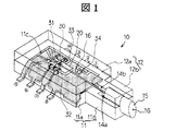
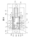
本実施形態1では、10Gb/sの送信用光通信モジュールに本発明を適用した例について説明する。本実施形態1の送信用光通信モジュール10は、図1及び図5に示すように、パッケージケース11と、このパッケージケース11を塞ぐように重ねられ、かつ接合材によって固定されるキャップ12とによってパッケージ(封止体)13が形成されている。パッケージケース11及びキャップ12はいずれもプラスチックで形成されている。プラスチックとしては、例えば、全芳香ポリエステルで形成されている。パッケージケース11及びキャップ12は外形が略同じとなっている。
【0025】
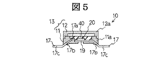
パッケージケース11及びキャップ12は、ともに矩形状の本体部11a,12aと、この本体部11a,12aの一端中央から長細く突出するガイド部11b,12bとからなっている(図1及び図2参照)。パッケージケース11の本体部11aは上部が開口(開口部11c)した箱型構造となっている。前記ガイド部11bから本体部11aの開口部に至る部分には、中央に溝14a,14bが設けられ、光ファイバケーブル15及びこの光ファイバケーブル15の先端側に露出した光ファイバ16を案内するようになっている(図2参照)。この光ファイバケーブル15及び光ファイバ16を案内する溝はキャップ12の下面にも対応して設けられている。キャップ12はパッケージケース11の開口部分や溝を塞ぐ板状となっている。光ファイバケーブル15はその中心を光ファイバ16が貫いている。光ファイバ16はジャケット等によって被覆される構造になっている。光ファイバ16は、図示はしないが、5μm直径のコアと、このコアを覆う125μm直径のクラッドとからなっている。この光ファイバ16を光ファイバ芯線とも呼称する。
【0026】
パッケージケース11の底面両側からは複数のリード17が突出している。また、これが本発明の特徴の一つであるが、これらのリード17は、図1及び図5に示すように、パッケージケース11の開口部11cからパッケージケース11の底面の両側縁近傍に亘って延在し、パッケージケース11の底面からパッケージケース11の外側に突出した後は屈曲してパッケージケース11の底面に平行に延在している。即ち、リード17は、開口部11cの内底に沿って延在する平坦面部17aと、開口部11cから底面に向かって延在する傾斜面部17bと、屈曲してパッケージケース11の底面に平行に延在する実装部17cとからなっている。パッケージ13におけるリード17の延在構造は、図5に示すように、いわゆるガルウィング型となっている。このようなリード構造にすることによってリードの長さは短くなり、リードインダクタンスの低減が図れる。
【0027】
一例であるが、パッケージ13の本体部11aの長さは13.0mm、ガイド部11bの長さは9.0mm、本体部11aの幅は7.4mm、パッケージ13の厚さは3.0mmである。また、リード17の下面の実装面からパッケージ13の上面までの高さは3.0mmである。
【0028】
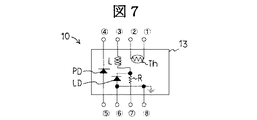
本実施形態1では、リード17はパッケージ13の両側にそれぞれ4本設けられている。そして、図1乃至図4及び図8に示すように、リード17の近傍にそれぞれ▲1▼〜▲8▼の数字のいずれかが記載されている。これはピン(リード)番号を示すものであり、図7の等価回路のピン番号と一致するものである。
【0029】
ここで本実施形態1の送信用光通信モジュール10の回路構成について図7を参照して説明する。パッケージ13内には、レーザダイオード(LD),モニター用のフォトダイオード(PD),温度検出用のサーミスタ(Th)、インダクタ(L:チップインダクタ)、抵抗(R:調整抵抗)が組み込まれている。
【0030】
ピン▲1▼とピン▲2▼間にサーミスタ(Th)が接続され、ピン▲4▼とピン▲5▼はフォトダイオード(PD:受光素子)が接続され、ピン▲4▼はPD用のカソード電極となり、ピン▲5▼はPD用のアノード電極となる。ピン▲6▼はLD(半導体レーザ)に接続され、LD用のアノード電極となり、グランド(GND)電位にされる。ピン▲3▼はインダクタ(L)を介してLDに接続され、DCバイアス用のカソード電極となる。ピン▲7▼は抵抗(R:調整抵抗)を介してLDに接続され、高周波信号を入力(高周波信号入力部)するカソード電極となる。ピン▲8▼はグランド端子である。
【0031】
本実施形態1のパッケージケース11においては、図1及び図4に示すように、パッケージケース11の開口部11cの内底に幅広のリードベース19が設けられている。このリードベース19は、リード17形成時に同時に形成され、材質,板厚共にリードと同じものである。そして、このリードベース19は1本以上のリード17と一体となっている。本実施形態1ではリードベース19はピン▲2▼,ピン▲6▼,ピン▲8▼に一体となっている。これらピン▲2▼,ピン▲6▼,ピン▲8▼はグランドリードとなる。従って、リードベース19はグランド電位となる。
【0032】
リードベース19の中央には光素子等の部品が搭載される支持基板(プラットホーム)20が固定される。この支持基板20は、例えばシリコン基板で形成されている。そして、上面には絶縁膜(SiO2膜)が形成され、この絶縁膜上に所定パターンに導体層が形成されている。グランド電位とされない残りのピン▲1▼,ピン▲3▼,ピン▲4▼,ピン▲5▼,ピン▲7▼を構成する5本のリード17は、その内端をリードベース19に接触させずかつ一部のリード17ではできるだけ支持基板20に近接した位置まで延在するようにパターニングされている。即ち、ピン▲4▼,ピン▲5▼,ピン▲7▼の内端は支持基板20に近接するようになる。
【0033】
また、これが本発明の特徴の一つであるが、ピン▲7▼の傾斜面部17bの内端側は他のリード17よりも長くなり、従って、ピン▲7▼の平坦面部17aはリードベース19よりも高い位置に位置している。これは、支持基板20の上面に搭載される抵抗のワイヤ接続面になる電極面と、ピン▲7▼の平坦面部17aのワイヤ接続面とを同一高さまたは近似した高さとし、ワイヤの長さを短くし、ワイヤのインダクタンスを小さくするためである。この抵抗は半導体レーザ素子に接続されるものである。また、ピン▲7▼の平坦面部17aの先端と半導体レーザ素子との間に前記抵抗が位置し、半導体レーザ素子の高周波信号入力部となるピン▲7▼と半導体レーザ素子の電極に至るワイヤ,抵抗,ワイヤを経由する配線経路が最短となるように構成されている。これによってもワイヤのインダクタンスは低減されることになる。
【0034】
ここで、リードフレームを使用したパッケージケース11の製造方法について、図8及び図9を参照しながら説明する。パッケージケース11の製造においては、図8に示すようなリードフレーム21に対してトランスファモールディングを行ってパッケージケース11を形成する。図9に示すように、パッケージケース11にはリードフレーム21の一部が組み込まれる。
【0035】
リードフレーム21は、鉄−ニッケル系合金、例えばコバールからなる金属板であり、図8に示すようなパターンに形成されている。また、必要ならば表面に所定のメッキ膜を形成しておく。金属板は、エッチングまたはプレス成形によって形成され、一対の平行に延在する外枠22と、この外枠22を一定間隔で連結する内枠23とを有する。外枠22の中間部分にはガイド孔22aが設けられ、リードフレーム21の移送や位置決め用に利用される。
【0036】
一対の内枠23の内側からは、それぞれ4本のリード17が延在している。これら8本のリード17はピン▲1▼〜ピン▲8▼を構成する。8本のリード17は左寄りに配置されている。これは外枠22及び内枠23からなる矩形枠内に本体部11a及びガイド部11bからなるパッケージケース11が形成されることによる。ピン▲1▼〜ピン▲4▼及びピン▲5▼〜ピン▲8▼は一対の外枠22に連なるダム24で支持されている。これらダム24はパッケージケース11の本体部11aの縁に沿って所定距離離れて延在するとともに、途中で屈曲してガイド部11bの縁に沿って所定距離離れて延在する。
【0037】
ピン▲2▼,ピン▲6▼,ピン▲8▼の内端は本体部11aの開口部11cの内底面に形成されるリードベース19に連なっている。ピン▲2▼,ピン▲6▼,ピン▲8▼はグランドリードとなる。リードベース19の左端は細い連結片19aを介して外枠22に連結され、リードベース19の右端の両側部分は連結片19bを介してダム24に連結されている。これによりリードベース19はリードフレーム21に支持されている。ピン▲1▼,ピン▲3▼,ピン▲4▼,ピン▲5▼,ピン▲7▼の内端は、リードベース19との間に所定の空間を有して対峙している。
【0038】
図8において示すリード17を横切る2本の線は、リード17が開口部11cに位置する平坦面部17a、本体部11a内を貫通する傾斜面部17b、本体部11a(パッケージケース11)の底面から突出した後屈曲して形成される実装部17cを形成するための屈曲線25a,25bである。しかし、ピン▲7▼では、既に説明したように傾斜面部17bがパッケージケース11の開口部11c側に長く延在するようにするため、屈曲線はパッケージケース11の中心側により、屈曲線25b’となっている。
【0039】
図8において、各リード17を切断し、ダム24を切断除去し、パッケージケース11の本体部11aから外側に突出する連結片19a,19bを切断してリードベース19をリードフレーム21から分離させることによって図2に示すパッケージケース11を製造することができる。
【0040】
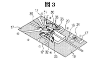
このようなパッケージケース11において、図1に示すように、パッケージケース11の溝14aには光ファイバケーブル15が挿入され、かつ溝14aの延長線上に設けられた溝14bには光ファイバケーブル15のジャケットが除去されて裸となった光ファイバ16が案内されている。そして、光ファイバ16の先端部分は、図3にも示すように支持基板20上に延在する。パッケージケース11の開口部11cの内底に固定される支持基板20の上面には、図示しないがV字断面のガイド溝が設けられ、このガイド溝に光ファイバ16が案内される。
【0041】
支持基板20の上面の中央には半導体レーザ素子(LD)30が固定されている。そして、半導体レーザ素子30の前方出射面から出射される前方出射光(レーザ光)が光ファイバ16のコアに取り込まれるようになる。この光軸合わせの後、光ファイバ16は図示しない接着剤で支持基板20及びパッケージケース11に固定され、光ファイバケーブル15はパッケージケース11に固定される。
【0042】
また、支持基板20の上面には、半導体レーザ素子30の後方出射面(レーザ光)を受光する受光素子(フォトダイオード)31が固定されている。また、支持基板20の上面には抵抗(調整抵抗)32が固定されている。図3及び図6に示すように、これら半導体レーザ素子30,受光素子31及び抵抗32はいずれも支持基板20の表面の導体層上に導電性の接着剤を介して固定されている。
【0043】
図3及び図6に示すように、開口部11c内に露出するリードベース19の所定箇所にはインダクタ(L)33及び温度検出用のサーミスタ(Th)34が導電性の接着剤を介して搭載されている。図3及び図6においては、リード17,リードベース19及び支持基板20の導電部分を点々を付して示してある。
【0044】
半導体レーザ素子30,受光素子31,インダクタ33,サーミスタ34は上面及び下面に電極を有する構造であり、抵抗32は上面に異なる電極を二つ有するものである。そして、各部品の電極,リード17,リードベース19及び支持基板20の表面の導体層(符号付けず)はそれぞれ導電性のワイヤ35で接続され、図7に示す回路が構成されている。ワイヤ35は、例えばAu線が使用されている。なお、一部の図では、各部品やワイヤ等の符号は図が微細でわかり難くなることから省略してある。
【0045】
インダクタ(L)33においては、渦巻き状に延在する導体層の中心部分はワイヤ35を介して半導体レーザ素子30の上部電極に電気的に接続され、渦の最終端部分はピン▲3▼に導電性のワイヤ35を介して電気的に接続されている。
【0046】
抵抗32は、絶縁性の基板の上面に抵抗層を有し、この抵抗層の両端上面にそれぞれ極性が異なる電極を有し、かつ基板の下面にも電極を有する構造になっている。従って、抵抗32の一方の電極は半導体レーザ素子30の一方の電極にワイヤ35を介して接続され、抵抗32の他方の電極はワイヤ35を介してピン▲7▼に接続されている。ピン▲7▼から半導体レーザ素子30の電極に至る配線経路は略直線的になり、最短の距離となることから、ワイヤのインダクタンスの低減が可能になる。また、ピン▲7▼のワイヤ接続面と抵抗32の電極面、即ちワイヤ接続面の高さは略一致した高さになっていることから、ワイヤ35の長さも短くなり、ワイヤのインダクタンスが低減されることになる。即ち、インピーダンスミスマッチを低減できる。
【0047】
また、実施形態1においては、支持基板20は、シリコンプラットフォームと呼称されるシリコン単結晶板で形成されている。支持基板20は半導体レーザチップやフォトダイオードチップ等の光素子や光ファイバを構成する石英等の熱膨張係数に近似した熱膨張係数を有する材質のものが使用される。従って、支持基板20は、シリコン以外に、窒化アルミニュウムまたはシリコンカーバイド等の絶縁性基板であってもよい。
【0048】
また、これが本発明の特徴の一つであるが、ピン▲7▼と、ピン▲7▼の両側のグランドリード(ピン▲6▼,ピン▲8▼)、さらにはパッケージケース11を形成するプラスチックは、25Ωにインピーダンス整合させたコプレーナ伝送線路となっている。この25Ωにインピーダンス整合させたコプレーナ伝送線路とするためには、信号線幅(ピン▲7▼)とグランド線(ピン▲6▼,ピン▲8▼)とのギャップの幅を適正に調整すれば得られる。
【0049】
また、パッケージケース11内には前記光ファイバ16で伝送される光に対して透明でありかつ耐湿性の保護膜40(図5参照)が充填されている。この保護膜40は、リードベース19,このリードベース19の周囲に延在するリード部分,支持基板20,半導体レーザ素子30,受光素子31,抵抗32,インダクタ33,サーミスタ34及び光ファイバ16等を被い、半導体レーザ素子30や受光素子31等の耐湿性向上が図られている。
【0050】
保護膜40は例えば、柔軟なシリコーンゲルである。なお、保護膜40は、シリコーンゲルに限らずシリコーンゴム,低応力エポキシ樹脂,アクリル樹脂,ウレタン樹脂等他のものであっても良い。
【0051】
半導体レーザ素子30から出射した前方出射光(レーザ光)はこの保護膜40を透過して光ファイバ16のコアに取り込まれ、後方出射光(レーザ光)はこの保護膜40を透過して受光素子31の受光面に到達する。保護膜40は、例えば柔軟なゲル状のシリコーン樹脂である。シリコーン樹脂の波長1.3μmにおける屈折率は1.4であり、光ファイバの屈折率と概ね整合している。なお、保護膜40は、シリコーン樹脂に限らずシリコーンゴム,低応力エポキシ樹脂,アクリル樹脂,ウレタン樹脂等他のものであっても良い。
【0052】
このような送信用光通信モジュール10の製造においては、最初に支持基板20に部品搭載を行った後、支持基板20をパッケージケース11の開口部11cの内底に露出するリードベース19上に固定する。また、パッケージケース11に必要を部品も搭載する。その後、所定部分を導電性のワイヤで接続し、ついで光ファイバ16を取り付ける。さらに、パッケージケース11の上面の支持基板20や各種部品等を保護膜40で被った後、キャップ12を取り付けて送信用光通信モジュール10を製造する。
【0053】
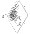
図10は送信用光通信モジュール10の実装状態を示す模式図である。即ち、実装基板45の上面のランド46上に送信用光通信モジュール10のリード17の実装部17cを重ね、半田等の接合材47で実装する。図11は実装基板45上に送信用光通信モジュール10を駆動制御するドライバIC50と送信用光通信モジュール10を実装した状態である。ドライバIC50の制御信号を伝送する配線51は送信用光通信モジュール10のピン▲7▼に接続され、高周波信号をピン▲7▼を介して送信用光通信モジュール10に入力する。
【0054】
図12は本実施形態1における3つの変形例を示す図であり、送信用光通信モジュール(光通信装置)10のパッケージケース11と、そのケース11を用いて製造した光通信装置の実装状態を示す図である。
【0055】
図12(a)はリード17の実装部17cの外端をパッケージケース11の側面と一致させたものである。この構造は実装面積の縮小が可能である。
【0056】
図12(b)はリード17の実装部17cの外端をパッケージケース11の外側に延在させたものである。またリード17の実装部17cはパッケージケース11の底面に沿って延在する構造になっている。
【0057】
図12(c)はリード17の実装部17cの外端をパッケージケース11の外側面よりも内側に位置させたものである。
【0058】
本実施形態1によれば以下の効果を有する。
(1)パッケージケース11の内部では、25Ωにインピーダンス整合したコプレーナ伝送線路が形成されているため高周波信号入力部を構成するリード(ピン▲7▼)における伝搬損失低減が図れ、送信用光通信モジュール(光通信装置)10の高周波特性が向上する。即ち、プラスチックパッケージ内部では低損失伝送線路が形成されることになる。
【0059】
(2)リード17は平坦面部17aと、この平坦面部17aに連なる傾斜面部17bと、この傾斜面部17bに連なる実装部17cとからなっていることから、リード17の長さを短くできリード17のインダクタンス低減が図れ、光通信装置の高周波特性が向上する。
【0060】
(3)半導体レーザ素子30の高周波信号入力部となるリード17(ピン▲7▼)は傾斜面部17bが他のリード17よりも長くなり、平坦面部17aの高さがリードベース19面よりも高くなり、平坦面部17aのワイヤ接続面とこのワイヤ接続面に接続されるワイヤ35の他端のワイヤ接続面が同一高さまたは近接した高さになっていることから、ワイヤ35の長さを短くでき、ワイヤ35のインダクタンス低減が図れ、光通信装置の高周波特性が向上する。
【0061】
(4)上記(1)乃至(3)により、インピーダンス整合及びインダクタンス低減から高周波特性が良好な光通信装置を提供することができる。
【0062】
(5)半導体レーザ素子30を搭載する支持基板20を支持するリードベース19の側方から上記(2)のようにリード長さが短くなるようにリード17(ピン▲7▼)を延在させていることから、換言するならば半導体レーザ素子30と高周波信号入力部となるリード17(ピン▲7▼)との配線経路を最短距離にできることから伝搬損失を低減することができ、光通信装置の高周波特性の改善が達成できる。
【0063】
(6)プラスチック製のパッケージ13構成とすることから光通信装置の製造コスト低減が図れる。
【0064】
(7)プラスチック製のパッケージケース及びリードによってコプレーナ伝送線路を形成するため、高速動作する光通信装置の低コスト化が達成できる。
【0065】
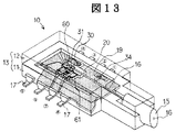
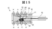
(実施形態2)
図13乃至図19は本発明の他の実施形態(実施形態2)である光通信装置(送信用光通信モジュール)に係わるである。図13は光通信装置の内部を透視した斜視図、図14は光通信装置の内部の一部を示す斜視図、図15は光通信装置のキャップを取り外した平面図、図16は光通信装置の断面図、図17は光通信装置の内部の一部を示す平面図である。また、図18は光通信装置の製造で用いるリードフレームにケースを形成した状態を示す平面図、図19は図17のB−B線に沿う断面図である。なお図面が見難くなることから、各図で符号の一部は省略してある。
【0066】
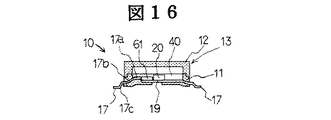
本実施形態2の光通信装置は、実施形態1の送信用光通信モジュール10と多くの点が同じであるが一部が異なる。即ち、実施形態1ではプラットホーム20上に抵抗32を配置したが、本実施形態2ではプラットホーム20の横にビァホール付き薄膜抵抗60を取り付けた偏平直方体からなる基板61(グランデッドコプレーナ伝送線路基板:GCPW基板)を配置している。この基板61の上面には、ビァホール付き薄膜抵抗60が搭載され、この薄膜抵抗60の一方の電極は半導体レーザ素子30側に位置し、ワイヤ35によって半導体レーザ素子30の上部電極に接続されている(図14参照)。薄膜抵抗60の他の電極は反対側に位置し、ワイヤ35を介してピン▲7▼を構成するリード17に接続されている。
【0067】
また、薄膜抵抗60の両側にはそれぞれ導体層62が設けられている。これら導体層62は符号は省略してあるがワイヤ35を介してグランドリードとなるピン▲6▼,ピン▲8▼に接続されるとともに、符号は省略してあるがワイヤ35を介してプラットホーム20の上面のグランド層(導体層)に接続されている。これにより、実施形態1と同様に25Ωにインピーダンス整合されたグランデッドコプレーナ伝送線路が形成される。従って、プラスチックパッケージ内部では低損失伝送線路が形成されることになる。
【0068】
リードベース19上に所定の厚さの基板61が固定され、この基板61上でのワイヤ接続面の高さが高くなることから、図14にも示すように、ピン▲5▼〜ピン▲8▼に至るリード部分は一段階段状に屈曲してピン▲6▼〜ピン▲8▼におけるワイヤ接続面高さを同じ高さにするように配慮されている。ワイヤボンディングを行う二点でのワイヤ接続面の高さが同じになることから、ワイヤ長を最も短くした接続が可能になり、ワイヤのインダクタンス低減が図れる。またインピーダンスミスマッチを低減できる。
【0069】
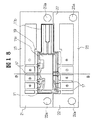
本実施形態2では、ピン▲5▼〜ピン▲8▼のリード部分(含むリードベース19)を、ピン▲1▼〜ピン▲4▼のリードの高さ(含むリードベース19)よりも一段高くするために、図18に示すように、パッケージケース11を製造する際使用するリードフレーム21を外枠22部分で切断分離させた構造になっている。
【0070】
また、本実施形態2では、図19及び図16に示すように、リード17の傾斜面部17bの下端の屈曲位置をパッケージケース11の本体部11aの中、即ち、プラスチック内とし、リード17をパッケージケース11の側面から外に突出させ、リード成形時には、図13及び図16に示すように、パッケージケース11の側面から側方に真っ直ぐ延在する部分をガルウィング状に折り曲げる構造になっている。この構造では、リード17の長さが、実施形態1の場合よりも長くなるが、ガルウィング型のリードの作り勝手がよくなるとともに、実装基板への半田接合が容易になり、かつ実装基板とパッケージとの熱膨張係数差に起因するストレス緩和に効果がある。
【0071】
本実施形態2の送信用光通信モジュール10は、高周波信号入力リードとなるピン▲7▼及びその両側のグランドリード(ピン▲6▼,ピン▲8▼)とリードベース19が分離することでグランドが分離するが、ビァホール付き薄膜抵抗付きグランデッドコプレーナ伝送線路(GCPW)基板を置くことで、非常に小さいインダクタンスでグランドリード(ピン▲6▼,ピン▲8▼)とリードベース19のグランドを接続させる。これにより、リードとパッケージ内の寄生容量に起因する共振を防止することができる。
【0072】
以上本発明者によってなされた発明を実施形態に基づき具体的に説明したが、本発明は上記実施形態に限定されるものではなく、その要旨を逸脱しない範囲で種々変更可能であることはいうまでもない。
【0073】
【発明の効果】
本願において開示される発明のうち代表的なものによって得られる効果を簡単に説明すれば、下記のとおりである。
【0074】
(1)高周波特性が優れた光通信装置を提供することができる。
【0075】
(2)伝搬損失が小さい光通信装置を提供することができる。
【0076】
(3)インピーダンス整合したインダクタンス値が低い光通信装置を提供することができる。
【0077】
(4)低コスト化が可能な光通信装置を提供することができる。
【図面の簡単な説明】
【図1】本発明の一実施形態(実施形態1)である光通信装置の内部を透視した斜視図である。
【図2】キャップを取り外した前記光通信装置の斜視図である。
【図3】前記光通信装置の内部の一部を示す斜視図である。
【図4】前記光通信装置のキャップを取り外した平面図である。
【図5】前記光通信装置の断面図である。
【図6】前記光通信装置の内部の一部を示す平面図である。
【図7】前記光通信装置の等価回路図である。
【図8】前記光通信装置の製造で用いるリードフレームにケースを形成した状態を示す平面図である。
【図9】図7のA−A線に沿う断面図である。
【図10】前記光通信装置の実装状態を示す模式図である。
【図11】前記光通信装置及びドライバICを光通信装置の実装基板に搭載した状態を示す模式的斜視図である。
【図12】本実施形態1における3つの変形例を示す図であり、光通信装置のケースと、そのケースを用いて製造した光通信装置の実装状態を示す図である。
【図13】本発明の他の実施形態(実施形態2)である光通信装置の内部を透視した斜視図である。
【図14】本実施形態2の光通信装置の内部の一部を示す斜視図である。
【図15】本実施形態2の光通信装置のキャップを取り外した平面図である。
【図16】本実施形態2の光通信装置の断面図である。
【図17】本実施形態2の光通信装置の内部の一部を示す平面図である。
【図18】本実施形態2の光通信装置の製造で用いるリードフレームにケースを形成した状態を示す平面図である。
【図19】図17のB−B線に沿う断面図である。
【符号の説明】
10…送信用光通信モジュール(光通信装置)、11…パッケージケース、11a,12a…本体部、11b,12b…ガイド部、11c…開口部、12…キャップ、13…パッケージ(封止体)、14a,14b…溝、15…光ファイバケーブル、16…光ファイバ、17…リード、17a…平坦面部、17b…傾斜面部、17c…実装部、19…リードベース、19a,19b…連結片、20…支持基板(プラットホーム)、21…リードフレーム、22…外枠、22a…ガイド孔、23…内枠、24…ダム、25a,25b,25b’…屈曲線、30…半導体レーザ素子、31…受光素子(フォトダイオード)、32…抵抗(調整抵抗)、33…インダクタ(L)、34…サーミスタ(Th)、35…ワイヤ、40…保護膜、45…実装基板、46…ランド、47…接合材、50…ドライバIC、51…配線、60…薄膜抵抗、61…基板、62…導体層。[0001]
TECHNICAL FIELD OF THE INVENTION
The present invention relates to an optical communication device, and particularly to a technology that is effective when applied to a manufacturing technology of an optical communication module for transmission or reception in optical communication.
[0002]
[Prior art]
Semiconductor lasers (laser diodes) are used as light sources for information processing devices and optical communication devices. In optical communication, optoelectronic devices such as a transmitting optical communication module and a receiving optical communication module are used. For example, Japanese Patent Application Laid-Open No. 10-307235 discloses a semiconductor laser module for transmission and a manufacturing technique thereof. This document discloses a semiconductor laser module in which a laser diode, a photodiode, and an optical fiber are mounted on a main surface of a silicon substrate fixed to an inner bottom surface of a package case (so-called passive alignment mounting), and the package case is sealed with a cap. Is described. The package case is formed by molding (molding) a plastic, and integrally forming an optical fiber installation groove and an optical fiber coating portion installation groove on the side of the package case with the pad portion with the lead terminal.
[0003]
Further, as a similar type of configuration, there is an optical communication module having a ceramic package structure in which a package has a hermetically sealed structure. As an optical communication module having this type of ceramic package structure, for example, Lucent Technologies, published by microelectronicsgroup, data sheet A laser module as described in DSO1-020OPTO (Replaces DS99-023LWP), December issue, 2000, P1 to P8 is known.
[0004]
[Problems to be solved by the invention]
The amount of data on the Internet (traffic), especially traffic flowing to the US mains, is increasing at a phenomenal pace. The development of high-speed and long-distance (for example, 10 Gbps, 80 km) transmission devices connecting large cities and within cities is proceeding at a rapid pace. On the other hand, there is also a demand for faster transmission devices such as an intra-office interface and a LAN connected to those transmission devices, which connect a short distance of 2 km or less.
[0005]
For widespread use of optical communication devices, cost reduction is an issue, and high-speed transmission devices of the 10 Gbps class are no longer an exception. A method of manufacturing a plastic package case by transfer molding using a lead frame is effective in reducing the cost of an optical communication device.
[0006]
Therefore, the present inventors have analyzed and studied an optical communication device using a plastic package case. As a result, the following facts were confirmed.
[0007]
It has been found that the prior art has a large lead and wire inductance and is not necessarily suitable for high-speed transmission. That is, the leads incorporated in the package case extend along the bottom of the package case and protrude outside the package case inside the package case, and bend and extend stepwise outside the package case at the tip outside the package case. The structure has a mounting portion suitable for surface mounting. As a result, the lead becomes longer and the inductance of the lead becomes larger.
[0008]
The leads and the lead base are formed by patterning a single flat metal plate. A support substrate is fixed on the lead base, and a semiconductor laser device and a resistor connected to the semiconductor laser device are fixed on the support substrate. One electrode of the resistor is connected to a lead via a wire. Therefore, the electrode surface of the resistor to which the wire is connected, that is, the wire connection surface of the resistor, is higher than the wire connection surface of the lead by the thickness of the support substrate and the semiconductor laser element. As a result, the length of the wire connecting the two points having different heights is increased by the difference in height, and the inductance of the wire is increased.
[0009]
An object of the present invention is to provide an optical communication device having excellent high frequency characteristics.
[0010]
Another object of the present invention is to provide an optical communication device having a small propagation loss.
[0011]
Another object of the present invention is to provide an optical communication device having a low inductance value that is impedance-matched.
[0012]
Another object of the present invention is to provide an optical communication device that can be reduced in cost.
[0013]
The above and other objects and novel features of the present invention will become apparent from the description of the present specification and the accompanying drawings.
[0014]
[Means for Solving the Problems]
The outline of a typical invention among the inventions disclosed in the present application will be briefly described as follows.
[0015]
(1) a package case made of plastic and having an opening on an upper surface;
A cap for closing the upper surface of the package case,
A plurality of metal leads that extend over the inside and outside of the package case and serve as electrode terminals,
A lead base disposed on the inner bottom of the package case and integrally formed with at least one or a plurality of the leads;
A support substrate fixed on the lead base and having a conductor pattern of a predetermined pattern on the upper surface,
One or more optical elements fixed on the support substrate,
The package case extends over the inside and outside of the package case, and has an inner end facing the one optical element (semiconductor laser element) so as to transmit and receive light to and from the semiconductor laser element. An optical fiber to be fixed;
One or more electronic components fixed to leads including the lead base in the package case;
An optical communication device comprising: a conductive wire that electrically connects each of the electrode of the optical element, the electrode of the electronic component, the conductive layer of the support substrate, and the lead as necessary,
Among the leads, the signal lead constituting the high-frequency signal input unit is arranged such that ground leads serving as ground electrodes are disposed on both sides thereof at predetermined intervals, and the signal lead and the ground leads on both sides and the signal lead and the ground lead are connected to each other. A coplanar transmission line whose impedance is matched by the package case portion to be supported is configured.
[0016]
The lead includes a flat surface portion located at the opening and connected to the wire, an inclined surface portion connected to the flat surface portion, and a mounting portion connected to the inclined surface portion and having a tip portion protruding from the package case. In the lead serving as a high-frequency signal input unit of the optical element (semiconductor laser element), the inclined surface portion is longer than other leads, the height of the flat surface portion is higher than the lead base surface, and the height of the flat surface portion is higher. The wire connection surface and the wire connection surface at the other end of the wire connected to the wire connection surface are at the same height or close to each other.
[0017]
According to the means of (1), (a) since a coplanar transmission line with impedance matching is formed inside the package case, propagation loss in a lead constituting the high-frequency signal input section can be reduced, and the high-frequency of the optical communication apparatus can be reduced. The characteristics are improved.
[0018]
(B) Since the lead comprises a flat surface portion, an inclined surface portion connected to the flat surface portion, and a mounting portion connected to the inclined surface portion, the length of the lead can be shortened, the inductance of the lead can be reduced, and the optical communication device can be reduced. The high frequency characteristics of are improved.
[0019]
(C) The lead serving as the high-frequency signal input portion of the semiconductor laser element has an inclined surface longer than the other leads, a flat surface higher than the lead base surface, and a flat surface connected to the wire. Since the wire connection surface at the other end of the wire connected to the surface is at the same height or close to the height, the length of the wire can be shortened, the inductance of the wire can be reduced, and the high frequency characteristics of the optical communication device Is improved.
[0020]
(D) According to the above (a) to (c), it is possible to provide an optical communication device having good high frequency characteristics from impedance matching and inductance reduction.
[0021]
(E) Since a coplanar transmission line is formed by a plastic package configuration and a plastic package case and leads, cost reduction of the optical communication device can be achieved.
[0022]
BEST MODE FOR CARRYING OUT THE INVENTION
Hereinafter, embodiments of the present invention will be described in detail with reference to the drawings. In all the drawings for describing the embodiments of the present invention, components having the same functions are denoted by the same reference numerals, and their repeated description will be omitted.
[0023]
(Embodiment 1)
1 to 11 are diagrams related to an optical communication module for transmission (optical communication device) according to an embodiment (Embodiment 1) of the present invention. 1 to 6 are diagrams relating to the structure of the transmission optical communication module, FIG. 7 is an equivalent circuit diagram of the transmission optical communication module, FIGS. 8 and 9 are diagrams relating to the manufacture of the transmission optical communication module, FIGS. FIG. 11 is a diagram related to the mounting state of the optical communication module for transmission.
[0024]
In the first embodiment, an example in which the present invention is applied to a 10 Gb / s transmission optical communication module will be described. As shown in FIGS. 1 and 5, the transmission
[0025]
The
[0026]
A plurality of
[0027]
For example, the length of the
[0028]
In the first embodiment, four leads 17 are provided on each side of the
[0029]
Here, the circuit configuration of the optical communication module for
[0030]
A thermistor (Th) is connected between pin (1) and pin (2), a photodiode (PD: light receiving element) is connected to pin (4) and pin (5), and a pin (4) is a cathode for PD. It becomes an electrode, and pin (5) becomes an anode electrode for PD. The pin (6) is connected to an LD (semiconductor laser), serves as an LD anode electrode, and is set to a ground (GND) potential. Pin (3) is connected to an LD via an inductor (L) and serves as a DC bias cathode electrode. The pin {circle around (7)} is connected to the LD via a resistor (R: adjusting resistor) and serves as a cathode electrode for inputting a high-frequency signal (high-frequency signal input section). Pin (8) is a ground terminal.
[0031]
In the
[0032]
A support substrate (platform) 20 on which components such as optical elements are mounted is fixed to the center of the
[0033]
This is one of the features of the present invention. The inner surface of the
[0034]
Here, a method of manufacturing the
[0035]
The
[0036]
Four leads 17 extend from the inside of the pair of
[0037]
The inner ends of the pins {circle around (2)}, {circle around (6)} and {circle around (8)} are connected to a
[0038]
The two lines crossing the
[0039]
In FIG. 8, each lead 17 is cut, the
[0040]
In such a
[0041]
A semiconductor laser element (LD) 30 is fixed at the center of the upper surface of the
[0042]
Further, a light receiving element (photodiode) 31 for receiving the rear emission surface (laser light) of the
[0043]
As shown in FIGS. 3 and 6, an inductor (L) 33 and a thermistor (Th) 34 for detecting temperature are mounted on predetermined portions of the
[0044]
The
[0045]
In the inductor (L) 33, the central part of the spirally extending conductor layer is electrically connected to the upper electrode of the
[0046]
The
[0047]
In the first embodiment, the
[0048]
This is one of the features of the present invention. The pin (7), the ground leads (pin (6), pin (8)) on both sides of the pin (7), and the plastic forming the
[0049]
The
[0050]
The
[0051]
Forward emitted light (laser light) emitted from the
[0052]
In the manufacture of such an optical communication module for
[0053]
FIG. 10 is a schematic diagram showing a mounting state of the
[0054]
FIG. 12 is a diagram showing three modified examples of the first embodiment, showing a
[0055]
FIG. 12A shows a state in which the outer end of the mounting
[0056]
FIG. 12 (b) shows an outer end of the mounting
[0057]
FIG. 12C shows an outer end of the mounting
[0058]
According to the first embodiment, the following effects can be obtained.
(1) Inside the
[0059]
(2) Since the
[0060]
(3) In the lead 17 (pin {circle around (7)}) serving as a high-frequency signal input portion of the
[0061]
(4) According to the above (1) to (3), it is possible to provide an optical communication device having good high-frequency characteristics from impedance matching and inductance reduction.
[0062]
(5) The lead 17 (pin {circle around (7)}) is extended from the side of the
[0063]
(6) Since the
[0064]
(7) Since the coplanar transmission line is formed by the package case and the lead made of plastic, the cost of the optical communication device operating at high speed can be reduced.
[0065]
(Embodiment 2)
13 to 19 relate to an optical communication device (transmission optical communication module) according to another embodiment (Embodiment 2) of the present invention. 13 is a perspective view showing the inside of the optical communication device, FIG. 14 is a perspective view showing a part of the inside of the optical communication device, FIG. 15 is a plan view of the optical communication device with a cap removed, and FIG. FIG. 17 is a plan view showing a part of the inside of the optical communication apparatus. FIG. 18 is a plan view showing a state in which a case is formed on a lead frame used in the manufacture of an optical communication device, and FIG. 19 is a cross-sectional view taken along line BB of FIG. Note that some of the reference numerals are omitted in each drawing because the drawings are difficult to see.
[0066]
The optical communication device of the second embodiment is similar in many respects to the optical communication module for
[0067]
[0068]
Since a
[0069]
In the second embodiment, the lead portions (including the lead base 19) of the pins (5) to (8) are one step higher than the lead heights (including the lead base 19) of the pins (1) to (4). For this purpose, as shown in FIG. 18, the
[0070]
In the second embodiment, as shown in FIGS. 19 and 16, the bending position of the lower end of the
[0071]
In the transmission
[0072]
Although the invention made by the inventor has been specifically described based on the embodiment, the present invention is not limited to the above embodiment, and various changes can be made without departing from the gist of the invention. Nor.
[0073]
【The invention's effect】
The effects obtained by the typical inventions among the inventions disclosed in the present application will be briefly described as follows.
[0074]
(1) An optical communication device having excellent high-frequency characteristics can be provided.
[0075]
(2) An optical communication device with small propagation loss can be provided.
[0076]
(3) An impedance-matched optical communication device with a low inductance value can be provided.
[0077]
(4) An optical communication device that can be reduced in cost can be provided.
[Brief description of the drawings]
FIG. 1 is a perspective view showing the inside of an optical communication device according to an embodiment (Embodiment 1) of the present invention.
FIG. 2 is a perspective view of the optical communication device with a cap removed.
FIG. 3 is a perspective view showing a part of the inside of the optical communication apparatus.
FIG. 4 is a plan view of the optical communication device with a cap removed.
FIG. 5 is a sectional view of the optical communication device.
FIG. 6 is a plan view showing a part of the inside of the optical communication apparatus.
FIG. 7 is an equivalent circuit diagram of the optical communication device.
FIG. 8 is a plan view showing a state in which a case is formed in a lead frame used in manufacturing the optical communication device.
FIG. 9 is a sectional view taken along line AA of FIG. 7;
FIG. 10 is a schematic diagram showing a mounting state of the optical communication device.
FIG. 11 is a schematic perspective view showing a state where the optical communication device and the driver IC are mounted on a mounting board of the optical communication device.
FIG. 12 is a diagram illustrating three modified examples of the first embodiment, illustrating a case of the optical communication device and a mounting state of the optical communication device manufactured using the case.
FIG. 13 is a perspective view showing the inside of an optical communication device according to another embodiment (Embodiment 2) of the present invention.
FIG. 14 is a perspective view showing a part of the inside of the optical communication apparatus according to the second embodiment.
FIG. 15 is a plan view of the optical communication device according to the second embodiment with a cap removed.
FIG. 16 is a cross-sectional view of the optical communication device according to the second embodiment.
FIG. 17 is a plan view showing a part of the inside of the optical communication apparatus according to the second embodiment.
FIG. 18 is a plan view showing a state where a case is formed in a lead frame used in manufacturing the optical communication device of the second embodiment.
FIG. 19 is a sectional view taken along the line BB of FIG. 17;
[Explanation of symbols]
DESCRIPTION OF
Claims (5)
前記パッケージケースの上面を塞ぐキャップと、
前記パッケージケースの内外に亘って延在し、外部は電極端子となる複数の金属からなるリードと、
前記パッケージケースの内底に配置され、前記リードの少なくとも1乃至複数と一体的に形成されたリードベースと、
前記リードベース上に固定されかつ上面に所定パターンの導体層を有する支持基板と、
前記支持基板上に固定される光素子と、
前記パッケージケースの内外に亘って延在するとともに、内端が前記光素子に対峙して前記光素子との間で光の授受を行うように前記支持基板上に固定される光ファイバと、
前記パッケージケース内の前記リードベースを含むリードに固定される1乃至複数の電子部品と、
前記光素子の電極,前記電子部品の電極,前記支持基板の導体層並びに前記リードのそれぞれを必要に応じて電気的に接続する導電性のワイヤとを有する光通信装置であって、
前記リードのうち高周波信号入力部を構成する信号リードはその両側に接地電極となるグランドリードが所定間隔離れるように配置され、前記信号リード及び前記両側のグランドリード並びに前記信号リードと前記グランドリードを支持する前記パッケージケース部分によってインピーダンス整合されたコプレーナ伝送線路が構成されていることを特徴とする光通信装置。A package case made of plastic and having an opening on an upper surface,
A cap for closing the upper surface of the package case,
A plurality of metal leads that extend over the inside and outside of the package case and serve as electrode terminals,
A lead base disposed on the inner bottom of the package case and integrally formed with at least one or a plurality of the leads;
A support substrate fixed on the lead base and having a conductor pattern of a predetermined pattern on the upper surface,
An optical element fixed on the support substrate,
An optical fiber that extends over the inside and outside of the package case, and is fixed on the support substrate so that an inner end faces the optical element and transmits and receives light to and from the optical element,
One or more electronic components fixed to leads including the lead base in the package case;
An optical communication device comprising: a conductive wire that electrically connects each of the electrode of the optical element, the electrode of the electronic component, the conductive layer of the support substrate, and the lead as necessary,
Of the leads, the signal lead constituting the high-frequency signal input unit is arranged on both sides thereof with ground leads serving as ground electrodes separated by a predetermined distance, and the signal lead and the ground leads on both sides and the signal lead and the ground lead are connected to each other. An optical communication device, wherein a coplanar transmission line whose impedance is matched by the package case portion to be supported is configured.
Priority Applications (1)
| Application Number | Priority Date | Filing Date | Title |
|---|---|---|---|
| JP2002365985A JP2004200331A (en) | 2002-12-18 | 2002-12-18 | Optical communication device |
Applications Claiming Priority (1)
| Application Number | Priority Date | Filing Date | Title |
|---|---|---|---|
| JP2002365985A JP2004200331A (en) | 2002-12-18 | 2002-12-18 | Optical communication device |
Publications (1)
| Publication Number | Publication Date |
|---|---|
| JP2004200331A true JP2004200331A (en) | 2004-07-15 |
Family
ID=32763329
Family Applications (1)
| Application Number | Title | Priority Date | Filing Date |
|---|---|---|---|
| JP2002365985A Pending JP2004200331A (en) | 2002-12-18 | 2002-12-18 | Optical communication device |
Country Status (1)
| Country | Link |
|---|---|
| JP (1) | JP2004200331A (en) |
Cited By (3)
| Publication number | Priority date | Publication date | Assignee | Title |
|---|---|---|---|---|
| JP2008066511A (en) * | 2006-09-07 | 2008-03-21 | Fuji Xerox Co Ltd | Optical transmission module, optical transmission module manufacturing method, and optical transmission device |
| WO2010146962A1 (en) * | 2009-06-16 | 2010-12-23 | 株式会社オートネットワーク技術研究所 | Optical communication module |
| JP5170080B2 (en) * | 2007-03-09 | 2013-03-27 | オムロン株式会社 | Package manufacturing method, package, and optical module |
-
2002
- 2002-12-18 JP JP2002365985A patent/JP2004200331A/en active Pending
Cited By (5)
| Publication number | Priority date | Publication date | Assignee | Title |
|---|---|---|---|---|
| JP2008066511A (en) * | 2006-09-07 | 2008-03-21 | Fuji Xerox Co Ltd | Optical transmission module, optical transmission module manufacturing method, and optical transmission device |
| JP5170080B2 (en) * | 2007-03-09 | 2013-03-27 | オムロン株式会社 | Package manufacturing method, package, and optical module |
| WO2010146962A1 (en) * | 2009-06-16 | 2010-12-23 | 株式会社オートネットワーク技術研究所 | Optical communication module |
| JP2011003610A (en) * | 2009-06-16 | 2011-01-06 | Autonetworks Technologies Ltd | Optical communication module |
| US9083137B2 (en) | 2009-06-16 | 2015-07-14 | Autonetworks Technologies, Ltd. | Optical communication module |
Similar Documents
| Publication | Publication Date | Title |
|---|---|---|
| US6164836A (en) | Opto-electronic hybrid integration platform, optical sub-module, opto-electronic hybrid integration circuit, and process for fabricating platform | |
| US6467972B2 (en) | Optical interconnection module | |
| TWI286387B (en) | LSI package provided with interface module, and transmission line header employed in the package | |
| JP3803596B2 (en) | Package type semiconductor device | |
| US7127142B2 (en) | Optical communication device | |
| US7044659B2 (en) | Optical communications module and method for producing the module | |
| JPWO2002089274A1 (en) | Optical communication device | |
| JP2004356233A (en) | Semiconductor laser module and semiconductor laser device | |
| JP4923542B2 (en) | Optical element stem and optical semiconductor device using the same | |
| JP2004093606A (en) | Optical module and optical transmitter | |
| JP3823102B2 (en) | Optical transmission module | |
| JPH11176966A (en) | Semiconductor element storage package | |
| JP2004200331A (en) | Optical communication device | |
| JP4105647B2 (en) | Semiconductor laser module and optical transmitter | |
| JP2008103774A (en) | High frequency optical transmission module, and optical transmitter | |
| JP2010034386A (en) | Optical semiconductor device | |
| JP3434473B2 (en) | Silicon platform for optical module | |
| JP2004200279A (en) | Photoelectric device | |
| JP2004184869A (en) | Photoelectronic apparatus | |
| JP4041226B2 (en) | Optical semiconductor device | |
| JP2000164970A (en) | Optical element module | |
| US6882761B2 (en) | Silicon platform for optical modules | |
| JP3769388B2 (en) | Optical semiconductor device | |
| JP2004235379A (en) | Optical package and optical module using the same | |
| JP4231166B2 (en) | Optical semiconductor device |