JP2004200418A - Integrated thin-film photoelectric conversion device, method of manufacturing the same, and glass substrate with transparent electrode - Google Patents
Integrated thin-film photoelectric conversion device, method of manufacturing the same, and glass substrate with transparent electrode Download PDFInfo
- Publication number
- JP2004200418A JP2004200418A JP2002367301A JP2002367301A JP2004200418A JP 2004200418 A JP2004200418 A JP 2004200418A JP 2002367301 A JP2002367301 A JP 2002367301A JP 2002367301 A JP2002367301 A JP 2002367301A JP 2004200418 A JP2004200418 A JP 2004200418A
- Authority
- JP
- Japan
- Prior art keywords
- film
- photoelectric conversion
- glass plate
- thin
- conversion unit
- Prior art date
- Legal status (The legal status is an assumption and is not a legal conclusion. Google has not performed a legal analysis and makes no representation as to the accuracy of the status listed.)
- Granted
Links
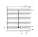
Images





Classifications
-
- H—ELECTRICITY
- H10—SEMICONDUCTOR DEVICES; ELECTRIC SOLID-STATE DEVICES NOT OTHERWISE PROVIDED FOR
- H10F—INORGANIC SEMICONDUCTOR DEVICES SENSITIVE TO INFRARED RADIATION, LIGHT, ELECTROMAGNETIC RADIATION OF SHORTER WAVELENGTH OR CORPUSCULAR RADIATION
- H10F77/00—Constructional details of devices covered by this subclass
- H10F77/10—Semiconductor bodies
- H10F77/16—Material structures, e.g. crystalline structures, film structures or crystal plane orientations
- H10F77/169—Thin semiconductor films on metallic or insulating substrates
- H10F77/1692—Thin semiconductor films on metallic or insulating substrates the films including only Group IV materials
-
- H—ELECTRICITY
- H10—SEMICONDUCTOR DEVICES; ELECTRIC SOLID-STATE DEVICES NOT OTHERWISE PROVIDED FOR
- H10F—INORGANIC SEMICONDUCTOR DEVICES SENSITIVE TO INFRARED RADIATION, LIGHT, ELECTROMAGNETIC RADIATION OF SHORTER WAVELENGTH OR CORPUSCULAR RADIATION
- H10F10/00—Individual photovoltaic cells, e.g. solar cells
- H10F10/10—Individual photovoltaic cells, e.g. solar cells having potential barriers
- H10F10/17—Photovoltaic cells having only PIN junction potential barriers
- H10F10/172—Photovoltaic cells having only PIN junction potential barriers comprising multiple PIN junctions, e.g. tandem cells
-
- H—ELECTRICITY
- H10—SEMICONDUCTOR DEVICES; ELECTRIC SOLID-STATE DEVICES NOT OTHERWISE PROVIDED FOR
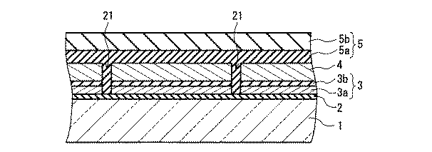
- H10F—INORGANIC SEMICONDUCTOR DEVICES SENSITIVE TO INFRARED RADIATION, LIGHT, ELECTROMAGNETIC RADIATION OF SHORTER WAVELENGTH OR CORPUSCULAR RADIATION
- H10F19/00—Integrated devices, or assemblies of multiple devices, comprising at least one photovoltaic cell covered by group H10F10/00, e.g. photovoltaic modules
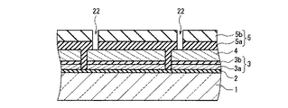
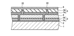
- H10F19/30—Integrated devices, or assemblies of multiple devices, comprising at least one photovoltaic cell covered by group H10F10/00, e.g. photovoltaic modules comprising thin-film photovoltaic cells
- H10F19/31—Integrated devices, or assemblies of multiple devices, comprising at least one photovoltaic cell covered by group H10F10/00, e.g. photovoltaic modules comprising thin-film photovoltaic cells having multiple laterally adjacent thin-film photovoltaic cells deposited on the same substrate
-
- Y—GENERAL TAGGING OF NEW TECHNOLOGICAL DEVELOPMENTS; GENERAL TAGGING OF CROSS-SECTIONAL TECHNOLOGIES SPANNING OVER SEVERAL SECTIONS OF THE IPC; TECHNICAL SUBJECTS COVERED BY FORMER USPC CROSS-REFERENCE ART COLLECTIONS [XRACs] AND DIGESTS
- Y02—TECHNOLOGIES OR APPLICATIONS FOR MITIGATION OR ADAPTATION AGAINST CLIMATE CHANGE
- Y02E—REDUCTION OF GREENHOUSE GAS [GHG] EMISSIONS, RELATED TO ENERGY GENERATION, TRANSMISSION OR DISTRIBUTION
- Y02E10/00—Energy generation through renewable energy sources
- Y02E10/50—Photovoltaic [PV] energy
- Y02E10/548—Amorphous silicon PV cells
Landscapes
- Photovoltaic Devices (AREA)
Abstract
【課題】透明導電膜の付着力を改善する効果がある2層構成の下地膜を有する透明電極を用いると、集積型薄膜光電変換装置の特性が十分に得られない。
【解決手段】 アルカリ成分含有ガラス板1と下地膜3との間に、連続した酸化珪素含有アルカリバリア膜2を形成し、酸化珪素含有膜3bに頼らず、ガラス板1からのアルカリ成分の拡散を抑制する。レーザー光の照射により、下地膜3は、透明導電膜4と共に分離溝21により複数に分割する。この集積型薄膜光電変換装置では、透明導電膜4上に、さらに薄膜光電変換ユニット5、金属電極膜6が配置される。
【選択図】 図1When a transparent electrode having a two-layered base film having an effect of improving the adhesion of a transparent conductive film is used, the characteristics of an integrated thin film photoelectric conversion device cannot be sufficiently obtained.
SOLUTION: A continuous silicon oxide-containing alkali barrier film 2 is formed between an alkali component-containing glass plate 1 and a base film 3, and diffusion of an alkali component from the glass plate 1 without relying on the silicon oxide-containing film 3b. Suppress. The base film 3 is divided into a plurality of parts by the separation groove 21 together with the transparent conductive film 4 by the irradiation of the laser beam. In this integrated thin film photoelectric conversion device, a thin film photoelectric conversion unit 5 and a metal electrode film 6 are further disposed on the transparent conductive film 4.
[Selection diagram] Fig. 1
Description
【0001】
【発明の属する技術分野】
本発明は、集積型薄膜光電変換装置の変換効率の改善に関し、特に透明電極付きガラス基板の改良に基づく集積型薄膜光電変換装置の光電変換効率および信頼性の改善に関するものである。
【0002】
【従来の技術】
いわゆるスーパーストレート型の集積型薄膜光電変換装置では、複数の短冊形状の薄膜光電変換セルがガラス基板上で相互に直列接続されている。薄膜光電変換セルは、透明電極付きガラス基板上への薄膜光電変換ユニットおよび金属電極膜の成膜およびパターニングにより形成される。各層のパターニングは、通常、レーザー光の照射により行われる。
【0003】
集積型薄膜光電変換装置では、薄膜光電変換ユニットにおいて光電変換に利用される光量を増やすために、光入射側の透明電極の表面に凹凸(表面テクスチャー)を付与し、この透明電極と裏面電極との間における光閉じ込め効果が利用される。透明電極付きガラス基板の光閉じこめ効果への寄与は、ヘイズ率を指標として評価できる。
【0004】
特許文献1には、表面が平滑なアルカリ含有ガラス板上に、膜厚150Å(15nm)以上の結晶性を有する金属酸化物層(例えばSnO2膜)と、この金属酸化物層の表面の凹凸を反映する膜厚を有するアルカリバリア層(SiO2膜)とをこの順に積層し、この2層の下地膜上にさらに膜厚5000Å(500nm)以上の透明導電膜(例えばフッ素をドープしたSnO2膜、以下、「SnO2:F膜」とも表記する)を形成した透明電極付きガラス基板が開示されている。この透明電極付きガラス基板は、透明電極として2層の下地膜と透明導電膜とを含み、下地膜の一部であるアルカリバリア層により、ガラス板からのアルカリ成分の拡散を抑制している。アルカリ成分の溶出は、透明導電膜や光電変換ユニットの変質や損傷を引き起こすからである。
【0005】
この基板において、結晶性を有する金属酸化物層は、アルカリバリア層の表面に凹凸を付与するために形成されている。凹凸を有するアルカリバリア層上に堆積した透明導電膜は、結晶粒がランダムな方向に成長しようとするためにその成長の初期段階ではアモルファス状態となる。このアモルファス状態の層は、結晶粒の成長に伴う結晶粒同士のせめぎ合いによって生じる膜の内部応力を緩和する。こうして、低抵抗化のために500nm以上にまで成長させても、透明導電膜におけるヘアクラックの発生や膜剥離が抑制される。
【0006】
【特許文献1】
特開2000−261013号公報([0009]〜[0013])
【0007】
【発明が解決しようとする課題】
特許文献1が開示する2層構成の下地膜は、透明導電膜のヘアクラックを防止し、その付着力を改善する効果がある。しかし、特許文献1が開示する透明電極付きガラス基板を用いて集積型薄膜光電変換装置を作製しても、透明電極付きガラス基板の特性(例えばヘイズ率)から期待される程度の光電変換特性が得られない。
【0008】
【課題を解決するための手段】
集積型薄膜光電変換装置の製造工程では、透明電極付きガラス基板上に薄膜光電変換ユニットなどを形成する前に、予め、透明電極を複数の短冊状に分割しておく必要がある。レーザー光の照射により透明電極を厚み方向にすべて分断すると、レーザー光のスキャンにより形成された分離溝を通じてガラス板からアルカリ成分が拡散する。透明導電膜のみを分断し、下地膜が連続膜として残るように分離溝を形成することは、例えば下地膜として単層のアルカリバリア層のみを有する透明電極(例えば、ガラス板側から、SiO2膜/SnO2:F膜)では、レーザー光の強度などの調整により十分に実現できる。
【0009】
しかし、上記2層構成の下地膜を備えた透明電極(例えば、ガラス板側から、SnO2膜/SiO2膜/SnO2:F膜)について、予め調整した一定の強度でレーザー光を照射しスキャンしても、サンプルによっては下地膜が分断されることがあった。また、同一のサンプル内において、分離溝が下地膜を分断する部分と分断しない部分とが混在する場合もあった。下地膜を単層から2層構成へと変更すると、透明電極を分断する分離溝の深さの制御が容易ではなくなる。
【0010】
この現象には、ガラス板から下地膜へのアルカリ成分の拡散による結晶性の金属酸化物層(例えばSnO2膜)の変質が関与している。ガラス板と2層構成の下地膜との間にさらにアルカリバリア膜を形成して下地膜へのアルカリ成分の拡散を抑制すると、分離溝の深さの不安定性は緩和した。さらに検討を進めたところ、2層構成の下地膜を備えた透明電極では、下地膜を連続膜として残存させると、透明導電膜を完全に分割したとしても、隣接する透明電極間における電気的絶縁を十分に確保できないことが見出された。
【0011】
そこで、本発明は、アルカリ成分含有ガラス板と、このガラス板上に上記ガラス板側から順次積層された下地膜、透明導電膜、薄膜光電変換ユニットおよび金属電極膜を含み、上記下地膜が、上記ガラス板側から順次積層された結晶性の金属酸化物層および酸化珪素含有層を含み、電気的に互いに直列に接続された複数のセルが形成されるように、上記透明導電膜、上記薄膜光電変換ユニットおよび上記金属電極膜がそれぞれ複数に分割されており、さらに、上記ガラス板と複数に分割された上記下地膜との間に、連続した酸化珪素含有アルカリバリア膜が形成されている集積型薄膜光電変換装置を提供する。
【0012】
本発明は、その別の側面から、アルカリ成分含有ガラス板と、このガラス板上に上記ガラス板側から順次積層された下地膜および透明導電膜を含み、上記下地膜が、上記ガラス板側から順次積層された結晶性の金属酸化物層および酸化珪素含有層を含み、さらに、上記ガラス板と上記下地膜との間に、酸化珪素含有アルカリバリア膜が形成された透明電極付きガラス基板を提供する。
【0013】
本発明は、また別の側面から、本発明の透明電極付きガラス基板にレーザー光を照射することにより上記透明導電膜および上記下地膜を複数に分割する工程と、複数に分割された上記透明導電膜上に薄膜光電変換ユニットを形成する工程と、レーザー光を照射することにより上記薄膜光電変換ユニットを複数に分割する工程と、複数に分割された上記薄膜光電変換ユニット上に金属電極膜を形成する工程と、レーザー光を照射して上記金属電極膜および上記薄膜光電変換ユニットを複数に分割することにより、電気的に互いに直列に接続された複数のセルを形成する工程と、を含み、上記ガラス板と上記下地膜との間に、酸化珪素含有アルカリバリア膜を形成する工程をさらに含み、上記透明導電膜および上記下地膜を分割する工程において、上記アルカリバリア膜を連続した膜として残す集積型薄膜光電変換装置の製造方法を提供する。
【0014】
【発明の実施の形態】
本発明の集積型薄膜光電変換装置の一形態では、互いに直列に接続された複数のセルが配置されるガラス板表面の全領域において、ガラス板と下地膜との間に、下地膜とは別にアルカリバリア膜が配置される。このアルカリバリア膜により、ガラス板から、透明導電膜、薄膜光電変換ユニットなどへのアルカリ成分の拡散が抑制される。アルカリ成分は、下地膜を構成する結晶性の金属酸化物層の光吸収を増加させるため、下地膜からも排除すべき成分である。こうして、集積型薄膜光電変換装置を構成する各膜の変質が抑制され、この装置の光電変換特性が向上する。また、ガラス板と下地膜との間にアルカリバリア膜を介在させると、下地膜の変質が抑制され、レーザー光のスキャンによる膜分割を安定して実施できる。さらに、透明導電膜と共に下地膜を分割することとしたため、隣接する透明電極間における電気的絶縁も確保しやすくなる。
【0015】
図1は、本発明の集積型薄膜光電変換装置の一形態を示す断面図である。この集積型薄膜光電変換装置は、アルカリ成分含有ガラス板であるソーダライムガラス板1を基板としている。この基板上に、アルカリバリア膜2、透明電極(下地膜3および透明導電膜4)、薄膜光電変換ユニット5、金属電極膜6、封止樹脂膜7、有機保護膜8が順次積層されている。
【0016】
この集積型薄膜光電変換装置では、薄膜光電変換ユニット5が分離溝23により分割されている。各セル10は、分離溝23により境界を画された薄膜光電変換ユニット5とこれを挟持する金属電極膜(裏面電極)6および透明電極(前面電極)3,4とを含み、裏面電極6および前面電極3,4は、分離溝22に充填された金属電極膜6により、隣接するセルの前面電極3,4および裏面電極6へとそれぞれ電気的に接続している。こうして、複数のセル10は互いに電気的に直列に接続されている。
【0017】
分離溝21は、透明導電膜4を貫通し、さらに下地膜3を分断するが、その底部はアルカリバリア膜2に接し、ガラス板1の表面には達していない。分離溝22,23の底部は、ともに透明導電膜4に接している。分離溝21,22,23は、互いに平行であって、かつそれぞれが隣接する同種の分離溝とも平行となるように、例えば分離溝21は隣接する分離溝21と平行となるように、形成するとよい。図2に示すように、集積型薄膜光電変換装置全体では、短冊状のセル10が一対の電極バスバー12,12を結ぶ方向13に沿って互いに直列に接続されている。この装置では、光電変換領域を確定するために絶縁溝11が形成され、バスバー12,12から出力が取り出される。図1は、図2のI−I断面図に相当する。
【0018】
ガラス板1としては、アルカリ成分を含むガラスであればよく、特に限定されないが、フロート法による大量に製造されるソーダライムガラス(フロートガラス)を用いれば足りる。このガラスは、SiO2、CaOなどに加え、Na2O、K2Oなどのアルカリ成分を含む。フロートガラスは、m角級の大面積電力用光電変換装置に特に適している。
【0019】
アルカリバリア膜2は、酸化珪素以外の成分を含んでいてもよいが、酸化珪素を主成分とする非晶質の被膜が適している。なお、本明細書において、「主成分」とは、慣用のとおり、過半を占める成分、具体的には50重量%以上を占める成分をいう。アルカリバリア膜2の膜厚は、アルカリ成分の拡散を十分に抑制するためには、15nm以上、さらに20nm以上が好ましいが、過度に厚膜化する必要はなく、例えば15nm〜50nmが好適である。
【0020】
下地膜3は、図示した形態では結晶性の金属酸化物層3aと酸化珪素含有層3bとからなる2層膜である。金属酸化物層3aには、結晶粒の成長によりその表面には凹凸が現れる。酸化珪素含有層3bは、金属酸化物層3aの表面の凹凸を反映した凹凸がその表面に形成されるように膜厚を選択することが好ましい。例えば、金属酸化物層3aの膜厚を15nm以上、酸化珪素含有層3bの膜厚を35nm以下とすると、特許文献1で確認されているとおり、透明導電膜4の付着力向上の効果が顕著となる。
【0021】
酸化珪素含有層3bが薄すぎると、この膜によるアルカリバリア機能は損なわれる。この機能を保持するための好ましい膜厚は、特許文献1に記載されているとおり、下地となる膜3aの表面凹凸を考慮すると、25nm以上である。しかし、ここでは下地膜3とは別にアルカリバリア膜2を形成しているため、酸化珪素含有層3bを25nm未満、さらには20nm以下にまで薄くしても、ガラス板1からのアルカリ成分の拡散を抑制できる。ただし、この層3bは、結晶性の金属酸化物層3aと透明導電膜4との結晶粒の連続性を断ち切るためには、厚さが10nm以上となるように形成することが好ましい。
【0022】
酸化珪素含有層3bの薄膜化とともに結晶性の金属酸化物層3aを厚膜化すると、下地膜3の表面の凹凸が顕著となる。この膜3の表面凹凸がある程度大きくなると、透明導電膜4の付着力の向上とともに、光閉じこめ効果も増大する。後述する実施例によると、下地膜3の表面凹凸がヘイズ率により評価して0.2%以上となると、集積型光電変換装置から得られる出力は向上した。なお、本明細書では、ヘイズ率は、一貫して、ガラス板側を光入射側として測定した値により表示する。
【0023】
透明導電膜4を形成する前の状態でヘイズ率を0.2%以上とするためには、金属酸化物層3aの膜厚を40nm以上、さらには50nm以上、例えば40nm〜300nmとするとよい。そして、酸化珪素含有膜3bの膜厚を、金属酸化物層3aの膜厚の50%以下として、膜3aの表面凹凸が緩和されすぎないようにするとよい。アルカリバリア膜2を介在させると下地膜3の設計自由度が増すため、酸化珪素含有層3bを薄膜化して、下地膜3全体をヘイズ増強膜として活用することが可能となる。
【0024】
結晶性の金属酸化物層3aは、例えば、酸化錫、酸化インジウム、酸化チタンおよび酸化亜鉛から選ばれる少なくとも1種を含む被膜とすればよい。酸化珪素含有層3bは、酸化珪素以外の成分を含んでいてもよいが、酸化珪素を主成分とする非晶質の被膜が適している。なお、下地膜3は、2層構成に限らず、3以上の層を含んでいても構わない。
【0025】
透明導電膜4としては、酸化亜鉛膜など導電性を示しうる各種酸化物を用いてもよいが、フッ素やアンチモンなどの不純物をドープして抵抗を下げた酸化錫膜が好ましい。透明導電膜4の膜厚は、電気抵抗を下げるために、500m以上、例えば500nm〜1200nm、さらには600nm〜1000nmとするとよい。不純物の濃度は、特に制限されないが、フッ素であれば0.03〜1.5モル%が適当である。下地膜3の表面凹凸を大きくすれば、透明導電膜4を形成した状態で測定したヘイズ率を12%以上にまで高くすることもできる。アルカリバリア膜2および下地膜3を形成した状態で測定した透明電極付きガラス基板のヘイズ率を0.2%以上とすると、透明導電膜4の膜厚を極度に厚膜化することなく、例えば上記範囲程度の膜厚で、12%以上、さらには15%以上のヘイズ率を有する透明電極付きガラス基板を得ることができる。
【0026】
薄膜光電変換ユニット5は、図示した形態では、非晶質光電変換ユニット5aと結晶質光電変換ユニット5bとをこの順に積層したタンデム型となっている。非晶質光電変換ユニット5aは、例えば透明導電膜4側から、p型シリコン系半導体層、シリコン系非晶質光電変換層、n型シリコン系半導体層をこの順に積層して形成すればよい。結晶質光電変換ユニット5bは、例えば非晶質光電変換ユニット5a側から、p型シリコン系半導体層、シリコン系結晶質光電変換層、n型シリコン系半導体層をこの順に積層して形成すればよい。ただし、薄膜光電変換ユニット5はタンデム型に限られるわけではない。なお、本明細書では、「結晶質」を、多結晶および微結晶を包含し、部分的に非晶質を含むことを許容する用語として使用する。
【0027】
非晶質光電変換ユニット5aと結晶質光電変換ユニット5bとは、互いに吸収波長域が異なっている。例えば、両光電変換ユニット5a,5bにおける光電変換層をそれぞれ非晶質シリコン層および結晶質シリコン層とすると、非晶質光電変換ユニット5aは波長550nm程度の光を、結晶質光電変換ユニット5bは波長900nm程度の光を最も効率的に吸収する。タンデム型の薄膜光電変換ユニットを用いると、異なる波長域の光を有効に利用できる。
【0028】
非晶質光電変換ユニット5aの厚さは0.1μm〜0.5μmが、結晶質光電変換ユニット5bの厚さは1μm〜5μmがそれぞれ好ましい。結晶質光電変換ユニット5bでは、非晶質光電変換ユニット5aよりも、光電変換層の光吸収係数が小さいため、このユニット5bの厚さは、非晶質光電変換ユニット4aの5倍〜10倍程度とするとよい。
【0029】
金属電極膜6は、裏面電極としての機能とともに、入射光を薄膜光電変換ユニット5へと反射する機能も有する。金属電極膜6は、銀、アルミニウムなどから形成するとよい。金属電極膜6の好ましい膜厚は、200nm〜400nmである。
【0030】
金属電極膜6およびこれよりもガラス板1側にある各膜は、封止樹脂膜7および有機保護膜8により封止され、保護されている。封止樹脂膜7は、有機保護膜8を接着する役割も担う。封止樹脂膜7としては、例えば、EVA(エチレン・酢酸ビニル共重合体)、PVB(ポリビニルブチラール)、PIB(ポリイソブチレン)、シリコーン樹脂などのフィルムを用いればよい。有機保護膜8は、例えば、ポリフッ化ビニルフィルム(例えば「テドラーフィルム」(登録商標))のようなフッ素樹脂系フィルム、PET(ポリエチレンテレフタレート)フィルムなどを用いればよい。これらの膜7,8は、単層であっても複数層からなっていてもよい。有機保護膜8として、アルミニウムなどからなる金属箔を含む多層膜、例えば金属箔を上記に例示した有機フィルムで挟持した3層構成、としてもよい。アルミニウム箔などの金属箔を用いると、水分の侵入を効果的に防止できる。これらの膜7,8は、真空ラミネート法により同時に貼り付けると、効率よく形成できる。
【0031】
本発明の透明電極付きガラス基板に含まれる各膜の形成方法は、特に制限されず、真空蒸着法、スパッタリング法、ゾル−ゲル法、液相析出法、焼き付け法、スプレー法、化学気相法(CVD法)などを適宜用いればよいが、被膜形成原料の熱分解を伴う方法(熱分解法)、例えば溶液スプレー法などの各種スプレー法、特に熱CVD法が適している。この透明電極付きガラス基板は、図3に示すように、アルカリ含有ガラス板1上に、アルカリバリア膜2、下地膜3a,3b、透明導電膜4をこの順に形成して作製される。
【0032】
アルカリバリア膜2として、熱分解法により酸化ケイ素膜を形成する場合には、モノシラン、ジシラン、ジクロロシラン、四塩化ケイ素などの無機ケイ素化合物;テトラメトキシシラン、テトラエトキシシラン、ジブトキシジアセトキシシランなどの有機ケイ素化合物をケイ素原料として用いればよい。ケイ素原料を酸化するための酸化原料としては、酸素、オゾン、アセトン、二酸化炭素などが適している。なお、モノシラン、ジシランなどのシランガスをケイ素原料とする場合には、エチレン、アセチレン、トルエン、エタンなどを添加すると、酸化ケイ素膜を安定して成膜できる。
【0033】
結晶性の金属酸化物層3aとして、熱分解法により酸化錫膜を形成する場合には、四塩化錫などの無機錫化合物、モノメチル錫トリクロライド、モノブチル錫トリクロライド(MBTC)、ジメチル錫ジクロライド(DMT)、ジブチル錫ジクロライド、テトラメチル錫、テトラブチル錫、ジブチル錫ジアセテート、ジオクチル錫ジアセテートなどの有機錫化合物を錫原料として用いればよい。錫原料を酸化するための酸化原料としては、乾燥空気、酸素、水蒸気、オゾンなどが適している。酸化珪素含有膜3bとして、熱分解法により酸化ケイ素膜を形成する場合には、上記に例示した原料を用いればよい。
【0034】
表面凹凸が大きい結晶性の金属酸化物層3aを得るためには、錫原料としてDMTを用いるCVD法による場合には、基板温度を高く(例えば600℃以上、特に650〜750℃)、水蒸気濃度を高く(被膜形成ガスにおける最大濃度の酸化原料とする;例えば5〜40モル%)、酸素濃度を低く(15モル%以下、特に10モル%以下、例えば5〜15モル%)、保持するとよい。
【0035】
透明導電膜4として、不純物をドープした酸化錫膜を形成する場合には、上記に例示した酸化錫膜の原料に加え、ドーピング剤として、フッ化水素、トリフルオロ酢酸、ブロモトリフルオロメタン、クロルジフルオロメタンなどのフッ素ドーピング剤;五塩化アンチモン、三塩化アンチモンなどのアンチモンドーピング剤を用いればよい。
【0036】
図3に示した透明電極付きガラス基板を量産する好ましい方法は、フロートガラス製造工程におけるガラスリボン上へのCVD法、いわゆるオンラインCVD法である。この方法を用いれば、ガラスリボンが有する熱を利用して被膜形成原料(被膜形成ガス)の熱分解を行うことができる。この方法を用いれば、フロートガラスのトップ面(フロートバスにおける溶融錫接触面であるボトム面とは反対側の表面)に、上記各膜2,3a,3b,4を極めて効率よく成膜できる。
【0037】
オンラインCVD法は、図9に示した装置により実施できる。この装置では、溶融炉31で溶解したガラス原料が錫フロート槽32へと流れ出し、この槽32内の錫浴34上で所定厚みを有するガラスリボン30へと成形される。槽32内のガラスリボン30上には、複数のコータ35が配置されており、これらのコータ35から被膜形成ガスが供給され、ガラスリボン上に、アルカリバリア膜、下地膜、透明導電膜が順次積層されていく。なお、ガラスリボン30の温度は、コータ35の直前で所定温度となるように、錫フロート槽32内に設置されたヒーターおよびクーラー(図示省略)により制御される。ガラスリボン30は、ロール36によって錫フロート槽32から引き上げられ、徐冷炉33で徐冷され、さらに下流側で所定の大きさに切断される。なお、コータの数は、図示した形態に制限されず、複数のコータを用いて単一の膜を形成してもよい。
【0038】
透明電極付きガラス基板における下地膜3a,3b、透明導電膜4をそれぞれ最上層とする状態でのヘイズ率の好ましい範囲は、以下のとおりである。
結晶性の金属酸化物層3a 0.2〜5%
酸化珪素含有層3b 0.2〜5%
透明導電膜4 12〜50%
【0039】
以下、図3に示した透明電極付きガラス基板を用いて集積型薄膜光電変換装置を作製する方法の一例を、図4〜図8を参照して説明する。まず、図4に示すように、透明電極付きガラス基板の透明導電膜4および下地膜3に、レーザー光を照射して分離溝21を形成する。レーザー光は、酸化珪素含有アルカリバリア膜2を分断しないように強度などを調整してスキャンされる。なお、結晶性の金属酸化物膜3aを確実に分断するために、この膜3aにおける自由電子キャリアを高めてレーザー光の吸収率を向上させてもよい。具体的には、結晶性の金属酸化物膜3aの抵抗率が1×10⁻¹Ω・cm以下となる程度にフッ素などの不純物をドープするとよい。
【0040】
次いで、図5に示すように、薄膜光電変換ユニット5を透明導電膜4上に形成する。分離溝21には、このユニットを構成する材料が充填され、隣接する透明導電膜4を絶縁する。薄膜光電変換ユニット5を構成する各層は、従来から知られている方法に従い、プラズマCVD法により形成すればよい。
【0041】
さらに、図6に示すように、レーザー光を照射して分離溝22を形成する。引き続き、図7に示すように、金属電極膜6を形成する。分離溝22は、その内部に充填された金属材料により、金属電極膜6と透明電極2,3とを導通させる接続溝となる。その後、図8に示すように、レーザー光の照射により形成される分離溝23により、各セル10が電気的に絶縁される。最後に、図1に示すように、封止樹脂膜7および有機保護膜8が形成されて集積型薄膜光電変換装置が得られる。
【0042】
【実施例】
以下に示す手順で、図1および図2と同様の構成を有する集積型薄膜光電変換装置を作製した。ここでは、アルカリ含有ガラス板1としてソーダライムガラスを用い、アルカリバリア膜2として非晶質SiO2膜を、結晶性の金属酸化物膜3aとしてSnO2膜を、酸化珪素含有膜3bとして非晶質SiO2膜を、透明導電膜4としてフッ素をドープしたSnO2(SnO2:F)膜をそれぞれ形成した。
【0043】
各膜は、図9と同様の装置を用いたオンラインCVD法によりガラスリボン上に順次堆積させた。ガラスリボンの厚さは5mmとした。最上流側のコータ直前のガラスリボンの温度は700〜750℃とした。このコータからは、モノシラン、エチレン、酸素、窒素からなる混合ガスを供給して非晶質SiO2アルカリバリア膜を形成した。2番目のコータからは、ジメチル錫ジクロライド(DMT)、水蒸気、酸素、ヘリウム、窒素からなる混合ガスを供給してSnO2膜を形成した。なお、この混合ガスにおける水蒸気および酸素の濃度は、それぞれ25モル%、7モル%とした。3番目のコータからは、モノシラン、エチレン、酸素、窒素からなる混合ガスを供給して非晶質SiO2膜を形成した。残りのコータからは、DMT、酸素、水蒸気、窒素、ヘリウム、フッ化水素からなる混合ガスを供給してSnO2:F膜を形成した。ガラスリボンは、下流側で切断して採板し、最終的には910mm×910mmの大きさへと切断した。
【0044】
各層の膜厚を(表1)に示す。膜厚は、混合ガスの供給速度および濃度を制御して調整した。SnO2:F膜(透明導電膜)の膜厚は、800nmで一定とした。(表1)における比較例では、最上流側のコータから窒素ガスのみを供給してSiO2アルカリバリア膜の形成を省略した。
【0045】
こうして得た各透明電極付きガラス基板について、ガラス板側を光入射側とするヘイズ率と、透明電極のシート抵抗値とを測定した。また、下地膜によるヘイズ率への寄与を調査するために、SnO2:F膜を形成しない以外は上記と同様にして、最上層をSiO2膜とする薄膜付きガラス板を得た。さらに、SnO2:F膜およびSiO2膜を形成しない以外は上記と同様にして、最上層をSnO2膜とする薄膜付きガラス板を得た。これらの薄膜付きガラス板についても、ヘイズ率を測定した。なお、ヘイズ率の測定は、曇価測定法(JIS K7105−1981)に準拠した。膜厚は、サンプルの断面の透過電子顕微鏡(TEM)像から平均値を計算することにより定めた。これらの結果を(表1)に併せて示す。
【0046】
【表1】
亜鉛粉末を触媒とした塩酸を用いたエッチングにより、透明電極付きガラス基板からSnO2:F膜のみを除去して最上層をSiO2膜とする薄膜付きガラス板を得た。こうして得た薄膜付きガラス板のヘイズ率は、SnO2:F膜の形成を省略して得たサンプルのヘイズ率((表1)のSiO2下地膜の欄に示された値)とほぼ同様となった。
【0048】
さらに、図4〜図8に示した手順により、上記各透明電極付きガラス基板から集積型薄膜光電変換装置を作製した。まず、YAG IRパルスレーザ(波長:1064nm)をSnO2:F膜側から照射しスキャンすることにより、SnO2:F膜、SiO2膜、SnO2膜のスクライブを行い、SiO2アルカリバリア膜を連続膜として残しつつ、これら3層の膜を複数の帯状体へと分割した。分離溝の幅および間隔は、それぞれ40μmおよび8.9mmとした。帯状体の数は100個である。
【0049】
透明電極を分割したガラス板を洗浄し、乾燥した後、プラズマCVD法により、SnO2:F膜上に、厚さ350nmの非晶質光電変換ユニットを形成した。このユニットは、p型層であるボロンドープ非晶質シリコンカーバイド層、光電変換層であるノンドープ非晶質シリコン層、n型層であるリンドープ微結晶シリコン層がこの順に積層されている。引き続き、プラズマCVD法により、非晶質光電変換ユニット上に膜厚2.5μmの結晶質光電変換ユニットを成膜した。このユニットには、p型層であるボロンドープ微結晶シリコン層、光電変換層であるノンドープ多結晶シリコン層、n型層であるリンドープ微結晶シリコン層がこの順に積層されている。
【0050】
次いで、YAG SHGパルスレーザー(波長:532nm)をガラス面側から照射しスキャンすることにより、非晶質光電変換ユニットおよび結晶質光電変換ユニットのスクライブを行い、これらユニットを複数の帯状体へと分割した。分離溝の幅は60μmとした。この分離溝と、SnO2:F膜などを分割する分離溝との中心間距離は100μmとした。
【0051】
さらに、これらユニット上に、スパッタリング法により、ZnO膜およびAg膜を順次成膜して金属裏面電極膜とした。引き続き、上記YAG SHGパルスレーザーをガラス面側から照射しスキャンすることにより、2つの光電変換ユニットおよび金属裏面電極膜を複数の帯状体へと分割した。分離溝の幅は60μmとした。この分離溝と、ユニットを分割する分離溝との中心間距離は100μmとした。
【0052】
発電領域を確定するために、上記YAG IRパルスレーザーをガラス板の周囲に沿ってスキャンすることにより、下地膜(SnO2膜、SiO2膜)、透明導電膜(SnO2:F膜)、薄膜光電変換ユニット、金属裏面電極膜に絶縁溝を形成し、さらに、 上記YAG SHGパルスレーザをガラス板の周囲に沿ってスキャンすることにより、薄膜光電変換ユニットおよび金属裏面電極膜に溝を形成した。その後、電極バスバーとして半田メッキ銅箔を取り付け、封止樹脂膜としてEVAシートを、有機保護膜としてフッ素樹脂系シート(「テドラー」(登録商標))を乗せ、真空ラミネート法を用いてこれらシートにより各膜を封止した。こうして、それぞれ8.9mm×890mmのサイズを有するハイブリッド型薄膜光電変換セルが、所定方向に100段直列に接続された集積型薄膜光電変換装置を得た。
【0053】
各集積型薄膜光電変換装置の光電変換特性を、光源としてキセノンランプおよびハロゲンランプを用いた放射照度100mW/cm2、AM1.5のソーラーシュミレータを用いて25℃で測定した。結果を(表2)に示す。各集積型薄膜光電変換装置は、AM1.5スペクトル下で、短絡電流が結晶質光電変換ユニットの光電変換層の膜厚により定まるいわゆるボトム律速の状態にあることが各サンプルから切り出した小面積サンプルの分光感度測定により確認された。
【0054】
さらに、各集積型薄膜光電変換装置のバスバー間に150Ωの負荷抵抗を接続し、受光面に疑似太陽光を照射しながら、85℃、85%の恒温恒湿槽内に5000時間設置し、受光面側から見た集積型薄膜光電変換装置の膜の変化を目視により確認した。目視による変化がない場合を「良好」、変色点が確認された場合を「不良」と判断した。結果を併せて(表2)に示す。
【0055】
【表2】
比較例の光電変換特性は、透明電極付きガラス基板のヘイズ率(17%)から予想されるよりも大きく劣っており、信頼性試験の結果も不良となった。比較例の透明電極付きガラス基板のTEM像では、図10に示すように、下地膜3を分断しガラス板1の表面にまで達する分離溝25と、透明導電膜4のみを分断する分離溝26とが観察された。同じ強度のレーザ光でスキャンした比較例において2種類の分離溝25,26が混在していたのは、ガラス板1からSnO2層3aへのアルカリ成分の拡散量の相違による。比較例において光電変換特性が大きく見劣りし、かつ信頼性も十分でないのは、分離溝26による透明電極の不十分な絶縁、ガラス板1から分離溝25を通じて拡散したアルカリ成分による各膜の劣化、さらにはアルカリ成分によるSnO2膜3aの変質によると考えられる。
【0057】
実施例8では、SiO2アルカリバリア膜が形成されているため、比較例よりも良好な光電変換特性が得られた。実施例8でも信頼性試験の結果は不良であるが、比較例よりも変色の程度は小さかった。しかし、このSiO2アルカリバリア膜は厚さが15nm未満であるため、アルカリ成分のバリア効果が十分ではなく、光電変換特性は十分に改善していない。
【0058】
(表1)における実施例1〜3の対比により、透明電極付きガラス基板のヘイズ率に寄与しうるSnO2膜の膜厚は40nm以上であることが確認できた。実施例3以降では、SiO2膜の膜厚もSnO2膜の表面凹凸による効果を阻害しない範囲に抑えられている。(表2)のとおり、透明電極付きガラス基板のヘイズ率の上昇に伴って集積型薄膜光電変換装置の短絡電流は増加した。短絡電流の増加は、ヘイズ率が8〜15%の間において特に顕著となった。
【0059】
【発明の効果】
以上詳細に説明したとおり、本発明では、集積型薄膜光電変換装置に適した透明電極構造を採用しているため、この装置の光電変換特性を向上させ、その信頼性を改善し、さらには、透明電極の一部である下地膜のレーザー光による加工の安定性を増し、ひいては集積型薄膜光電変換装置の製造効率を高めることができる。
【図面の簡単な説明】
【図1】本発明の集積型薄膜光電変換装置の一形態を示す断面図である。
【図2】図1の集積型薄膜光電変換装置の平面図である。
【図3】本発明の透明電極付きガラス基板の一形態を示す断面図である。
【図4】本発明の集積型薄膜光電変換装置の製造方法の一例における一工程を説明するための断面図である。
【図5】図4に引き続いて行われる一工程を説明するための断面図である。
【図6】図5に引き続いて行われる一工程を説明するための断面図である。
【図7】図6に引き続いて行われる一工程を説明するための断面図である。
【図8】図7に引き続いて行われる一工程を説明するための断面図である。
【図9】本発明の透明電極付きガラス基板の製造に適した装置の構成を示す図である。
【図10】従来の集積型薄膜光電変換装置を示す断面図である。
【符号の説明】
1 アルカリ成分含有ガラス板
2 酸化珪素含有アルカリバリア膜
3 下地膜
3a 結晶性の金属酸化物層
3b 酸化珪素含有層
4 透明導電膜
5 薄膜光電変換ユニット
5a 非晶質光電変換ユニット
5b 結晶質光電変換ユニット
6 金属電極膜
7 封止樹脂膜
8 有機保護膜
21,22,23 分離溝[0001]
TECHNICAL FIELD OF THE INVENTION
The present invention relates to an improvement in the conversion efficiency of an integrated thin film photoelectric conversion device, and more particularly to an improvement in the photoelectric conversion efficiency and reliability of an integrated thin film photoelectric conversion device based on an improvement in a glass substrate with a transparent electrode.
[0002]
[Prior art]
In a so-called superstrate integrated thin film photoelectric conversion device, a plurality of strip-shaped thin film photoelectric conversion cells are connected in series on a glass substrate. The thin film photoelectric conversion cell is formed by forming and patterning a thin film photoelectric conversion unit and a metal electrode film on a glass substrate with a transparent electrode. The patterning of each layer is usually performed by irradiation with a laser beam.
[0003]
In the integrated thin-film photoelectric conversion device, in order to increase the amount of light used for photoelectric conversion in the thin-film photoelectric conversion unit, the surface of the transparent electrode on the light incident side is provided with irregularities (surface texture). The light confinement effect between the two is utilized. The contribution of the glass substrate with a transparent electrode to the light confinement effect can be evaluated using the haze ratio as an index.
[0004]
[0005]
In this substrate, the metal oxide layer having crystallinity is formed to provide irregularities on the surface of the alkali barrier layer. The transparent conductive film deposited on the alkali barrier layer having the irregularities is in an amorphous state at an initial stage of the growth because crystal grains tend to grow in random directions. This layer in the amorphous state relieves the internal stress of the film caused by the interference between the crystal grains accompanying the growth of the crystal grains. In this manner, even when the transparent conductive film is grown to a thickness of 500 nm or more for lowering the resistance, generation of hair cracks and peeling of the transparent conductive film are suppressed.
[0006]
[Patent Document 1]
JP 2000-261013 A ([0009] to [0013])
[0007]
[Problems to be solved by the invention]
The two-layered base film disclosed in
[0008]
[Means for Solving the Problems]
In the manufacturing process of an integrated thin film photoelectric conversion device, it is necessary to divide the transparent electrode into a plurality of strips in advance before forming a thin film photoelectric conversion unit or the like on a glass substrate with a transparent electrode. When the transparent electrode is completely cut in the thickness direction by the irradiation of the laser beam, the alkali component diffuses from the glass plate through the separation groove formed by the scanning of the laser beam. Forming the separation groove so as to separate only the transparent conductive film and leave the underlying film as a continuous film is performed, for example, by using a transparent electrode having only a single alkali barrier layer as the underlying film (for example, from the glass plate side,
[0009]
However, a transparent electrode provided with the two-layered base film (for example, SnO Two Film / SiO Two Membrane / SnO Two : F film), the base film was sometimes cut off depending on the sample even when scanning was performed by irradiating a laser beam with a predetermined intensity adjusted in advance. Further, in the same sample, a part where the separation groove divides the base film and a part where the separation groove does not divide may be mixed. When the base film is changed from a single layer to a two-layer structure, it is not easy to control the depth of the separation groove separating the transparent electrode.
[0010]
This phenomenon includes a crystalline metal oxide layer (for example,
[0011]
Therefore, the present invention includes an alkali component-containing glass plate, and a base film, a transparent conductive film, a thin film photoelectric conversion unit, and a metal electrode film sequentially laminated on the glass plate from the glass plate side, wherein the base film is The transparent conductive film and the thin film including a crystalline metal oxide layer and a silicon oxide-containing layer sequentially stacked from the glass plate side, so that a plurality of cells electrically connected to each other in series are formed. The photoelectric conversion unit and the metal electrode film are each divided into a plurality, and further, a continuous silicon oxide-containing alkali barrier film is formed between the glass plate and the plurality of divided base films. A thin film photoelectric conversion device is provided.
[0012]
The present invention includes, from another aspect thereof, a glass plate containing an alkali component, a base film and a transparent conductive film sequentially laminated on the glass plate from the glass plate side, and the base film is formed from the glass plate side. Provided is a glass substrate with a transparent electrode including a crystalline metal oxide layer and a silicon oxide-containing layer sequentially laminated, and further having a silicon oxide-containing alkali barrier film formed between the glass plate and the base film. I do.
[0013]
From another aspect, the present invention provides a step of dividing the transparent conductive film and the base film into a plurality by irradiating the glass substrate with a transparent electrode of the present invention with a laser beam; A step of forming a thin film photoelectric conversion unit on the film, a step of dividing the thin film photoelectric conversion unit into a plurality by irradiating a laser beam, and forming a metal electrode film on the plurality of divided thin film photoelectric conversion units And irradiating a laser beam to divide the metal electrode film and the thin-film photoelectric conversion unit into a plurality, thereby forming a plurality of cells electrically connected in series to each other, A step of forming a silicon oxide-containing alkali barrier film between the glass plate and the base film, wherein the step of dividing the transparent conductive film and the base film To provide a manufacturing method of an integrated thin film photoelectric conversion device to leave a continuous film of the alkali barrier film.
[0014]
BEST MODE FOR CARRYING OUT THE INVENTION
In one embodiment of the integrated thin-film photoelectric conversion device of the present invention, the entire region of the glass plate surface where a plurality of cells connected in series are arranged, between the glass plate and the base film, separately from the base film. An alkali barrier film is provided. With the alkali barrier film, diffusion of the alkali component from the glass plate to the transparent conductive film, the thin-film photoelectric conversion unit, and the like is suppressed. The alkali component is a component that should be excluded from the base film in order to increase the light absorption of the crystalline metal oxide layer constituting the base film. Thus, the quality of each film constituting the integrated thin film photoelectric conversion device is suppressed, and the photoelectric conversion characteristics of the device are improved. In addition, when an alkali barrier film is interposed between the glass plate and the base film, deterioration of the base film is suppressed, and film division by scanning with laser light can be stably performed. Further, since the base film is divided together with the transparent conductive film, electrical insulation between adjacent transparent electrodes can be easily secured.
[0015]
FIG. 1 is a cross-sectional view showing one embodiment of the integrated thin-film photoelectric conversion device of the present invention. This integrated thin-film photoelectric conversion device uses a soda-
[0016]
In this integrated type thin film photoelectric conversion device, the thin film
[0017]
The
[0018]
The
[0019]
The
[0020]
The
[0021]
If the silicon oxide-containing
[0022]
When the thickness of the crystalline
[0023]
In order to make the haze ratio 0.2% or more before the formation of the transparent
[0024]
The crystalline
[0025]
As the transparent
[0026]
In the illustrated embodiment, the thin-film
[0027]
The amorphous
[0028]
The thickness of the amorphous
[0029]
The
[0030]
The
[0031]
The method for forming each film included in the glass substrate with a transparent electrode of the present invention is not particularly limited, and includes a vacuum deposition method, a sputtering method, a sol-gel method, a liquid deposition method, a baking method, a spray method, and a chemical vapor method. (CVD method) or the like may be used as appropriate, but a method involving thermal decomposition of a film forming raw material (thermal decomposition method), for example, various spray methods such as a solution spray method, and particularly a thermal CVD method is suitable. As shown in FIG. 3, the glass substrate with a transparent electrode is manufactured by forming an
[0032]
When a silicon oxide film is formed as the
[0033]
When a tin oxide film is formed by a thermal decomposition method as the crystalline
[0034]
In order to obtain the crystalline
[0035]
When a tin oxide film doped with an impurity is formed as the transparent
[0036]
A preferred method for mass-producing the glass substrate with a transparent electrode shown in FIG. 3 is a CVD method on a glass ribbon in a float glass manufacturing process, a so-called online CVD method. By using this method, it is possible to thermally decompose the film forming raw material (film forming gas) using the heat of the glass ribbon. By using this method, each of the
[0037]
The online CVD method can be performed by the apparatus shown in FIG. In this apparatus, a glass raw material melted in a
[0038]
The preferred range of the haze ratio in the state where the
Crystalline
Silicon
Transparent
[0039]
Hereinafter, an example of a method for manufacturing an integrated thin-film photoelectric conversion device using the glass substrate with a transparent electrode shown in FIG. 3 will be described with reference to FIGS. First, as shown in FIG. 4, the transparent
[0040]
Next, as shown in FIG. 5, a thin-film
[0041]
Further, as shown in FIG. 6, the
[0042]
【Example】
According to the following procedure, an integrated thin-film photoelectric conversion device having a configuration similar to that of FIGS. 1 and 2 was manufactured. Here, soda lime glass is used as the alkali-containing
[0043]
Each film was sequentially deposited on a glass ribbon by an online CVD method using an apparatus similar to that shown in FIG. The thickness of the glass ribbon was 5 mm. The temperature of the glass ribbon immediately before the coater on the most upstream side was 700 to 750 ° C. From this coater, a mixed gas consisting of monosilane, ethylene, oxygen, and nitrogen is supplied to form an
[0044]
The thickness of each layer is shown in (Table 1). The film thickness was adjusted by controlling the supply rate and concentration of the mixed gas. SnO Two : The thickness of the F film (transparent conductive film) was fixed at 800 nm. In the comparative example in (Table 1), only the nitrogen gas was supplied from the coater on the most upstream side, and SiO Two The formation of the alkali barrier film was omitted.
[0045]
For each of the thus obtained glass substrates with a transparent electrode, the haze ratio with the glass plate side as the light incident side and the sheet resistance of the transparent electrode were measured. In order to investigate the contribution of the underlayer to the haze ratio, SnO Two : In the same manner as above except that the F film is not formed, Two A glass plate with a thin film as a film was obtained. Furthermore, SnO Two : F film and SiO Two Except that no film is formed, the uppermost layer is made of SnO Two A glass plate with a thin film as a film was obtained. The haze ratio of these glass plates with a thin film was also measured. The measurement of the haze ratio was based on the haze value measurement method (JIS K7105-1981). The film thickness was determined by calculating an average value from a transmission electron microscope (TEM) image of a cross section of the sample. These results are also shown in (Table 1).
[0046]
[Table 1]
By etching using hydrochloric acid using zinc powder as a catalyst, SnO was removed from the glass substrate with a transparent electrode. Two : Only the F film is removed and the uppermost layer is made of SiO. Two A glass plate with a thin film as a film was obtained. The haze ratio of the glass plate with a thin film thus obtained is SnO Two : Haze ratio of sample obtained without formation of F film (SiO of (Table 1)) Two (The value shown in the column of the base film).
[0048]
Further, according to the procedure shown in FIGS. 4 to 8, an integrated thin-film photoelectric conversion device was manufactured from the above-mentioned glass substrate with a transparent electrode. First, a YAG IR pulsed laser (wavelength: 1064 nm) was Two : By irradiating and scanning from the F film side, SnO Two : F film, SiO Two Membrane, SnO Two Scribe the film, Two These three layers were divided into a plurality of strips while leaving the alkali barrier film as a continuous film. The width and spacing of the separation grooves were 40 μm and 8.9 mm, respectively. The number of strips is 100.
[0049]
After cleaning and drying the glass plate from which the transparent electrode was divided, SnO was formed by plasma CVD. Two : An amorphous photoelectric conversion unit having a thickness of 350 nm was formed on the F film. In this unit, a boron-doped amorphous silicon carbide layer as a p-type layer, a non-doped amorphous silicon layer as a photoelectric conversion layer, and a phosphorus-doped microcrystalline silicon layer as an n-type layer are stacked in this order. Subsequently, a 2.5 μm-thick crystalline photoelectric conversion unit was formed on the amorphous photoelectric conversion unit by a plasma CVD method. In this unit, a boron-doped microcrystalline silicon layer as a p-type layer, a non-doped polycrystalline silicon layer as a photoelectric conversion layer, and a phosphorus-doped microcrystalline silicon layer as an n-type layer are stacked in this order.
[0050]
Then, the amorphous photoelectric conversion unit and the crystalline photoelectric conversion unit are scribed by irradiating a YAG SHG pulse laser (wavelength: 532 nm) from the glass surface and scanning, and these units are divided into a plurality of strips. did. The width of the separation groove was 60 μm. This separation groove and SnO Two : The distance between the center and the separation groove for dividing the F film or the like was 100 μm.
[0051]
Further, a ZnO film and an Ag film were sequentially formed on these units by a sputtering method to form a metal back electrode film. Subsequently, the two photoelectric conversion units and the metal back electrode film were divided into a plurality of strips by irradiating the YAG SHG pulse laser from the glass surface side and scanning. The width of the separation groove was 60 μm. The center-to-center distance between the separation groove and the separation groove for dividing the unit was 100 μm.
[0052]
In order to determine the power generation region, the YAG IR pulsed laser is scanned along the periphery of the glass plate to form a base film (SnO Two Film, SiO Two Film), transparent conductive film (SnO) Two : F film), the thin film photoelectric conversion unit, and an insulating groove formed in the metal back electrode film, and further, the YAG SHG pulse laser is scanned along the periphery of the glass plate to obtain the thin film photoelectric conversion unit and the metal back electrode film. A groove was formed in the groove. Thereafter, a solder-plated copper foil is attached as an electrode bus bar, an EVA sheet is placed as a sealing resin film, and a fluororesin sheet (“Tedlar” (registered trademark)) is placed as an organic protective film. Each film was sealed. Thus, an integrated thin-film photoelectric conversion device in which hybrid thin-film photoelectric conversion cells each having a size of 8.9 mm × 890 mm were connected in series in a predetermined direction in 100 stages was obtained.
[0053]
The photoelectric conversion characteristics of each integrated thin-film photoelectric conversion device were measured using an irradiance of 100 mW / cm using a xenon lamp and a halogen lamp as light sources. Two , AM1.5 at 25 ° C. using a solar simulator. The results are shown in (Table 2). Each integrated thin-film photoelectric conversion device is a small area sample cut out from each sample, under the AM1.5 spectrum, the short-circuit current is in a so-called bottom rate-determined state determined by the thickness of the photoelectric conversion layer of the crystalline photoelectric conversion unit. Was confirmed by the spectral sensitivity measurement.
[0054]
Further, a load resistance of 150Ω is connected between the bus bars of each integrated thin film photoelectric conversion device, and the light receiving surface is set in a constant temperature and humidity chamber at 85 ° C. and 85% for 5000 hours while illuminating the light receiving surface with pseudo sunlight. Changes in the film of the integrated thin-film photoelectric conversion device viewed from the surface side were visually confirmed. A case where there was no visual change was judged as “good”, and a case where a discoloration point was confirmed was judged as “poor”. The results are shown in Table 2 together.
[0055]
[Table 2]
The photoelectric conversion characteristics of the comparative example were much worse than expected from the haze ratio (17%) of the glass substrate with a transparent electrode, and the results of the reliability test were also poor. In the TEM image of the glass substrate with a transparent electrode of the comparative example, as shown in FIG. 10, a
[0057]
In Example 8,
[0058]
By comparison of Examples 1 to 3 in (Table 1), SnO which can contribute to the haze ratio of the glass substrate with a transparent electrode can be obtained. Two It was confirmed that the film thickness was 40 nm or more. In the third and subsequent embodiments, SiO Two The film thickness is SnO Two The effect is suppressed within a range that does not hinder the effect due to the surface unevenness of the film. As shown in Table 2, as the haze ratio of the glass substrate with a transparent electrode increased, the short-circuit current of the integrated thin-film photoelectric conversion device increased. The increase in the short-circuit current was particularly remarkable when the haze ratio was between 8 and 15%.
[0059]
【The invention's effect】
As described in detail above, in the present invention, since a transparent electrode structure suitable for an integrated thin film photoelectric conversion device is employed, the photoelectric conversion characteristics of this device are improved, the reliability thereof is improved, and further, The stability of processing of the base film, which is a part of the transparent electrode, with the laser beam can be increased, and the production efficiency of the integrated thin-film photoelectric conversion device can be increased.
[Brief description of the drawings]
FIG. 1 is a cross-sectional view illustrating one embodiment of an integrated thin-film photoelectric conversion device of the present invention.
FIG. 2 is a plan view of the integrated thin-film photoelectric conversion device of FIG.
FIG. 3 is a cross-sectional view showing one embodiment of a glass substrate with a transparent electrode of the present invention.
FIG. 4 is a cross-sectional view for explaining one step in an example of the method for manufacturing an integrated thin-film photoelectric conversion device of the present invention.
FIG. 5 is a cross-sectional view for explaining one step performed subsequently to FIG. 4;
FIG. 6 is a cross-sectional view for explaining one step performed subsequently to FIG. 5;
FIG. 7 is a cross-sectional view for explaining one step performed subsequently to FIG. 6;
FIG. 8 is a cross-sectional view for explaining one step performed subsequently to FIG. 7;
FIG. 9 is a view showing a configuration of an apparatus suitable for manufacturing a glass substrate with a transparent electrode according to the present invention.
FIG. 10 is a cross-sectional view showing a conventional integrated thin-film photoelectric conversion device.
[Explanation of symbols]
1 Glass plate containing alkali component
2 Alkali barrier film containing silicon oxide
3 Underlayer
3a Crystalline metal oxide layer
3b Silicon oxide containing layer
4 Transparent conductive film
5 Thin-film photoelectric conversion unit
5a Amorphous photoelectric conversion unit
5b Crystalline photoelectric conversion unit
6 Metal electrode film
7 Sealing resin film
8 Organic protective film
21,22,23 Separation groove
Claims (10)
前記下地膜が、前記ガラス板側から順次積層された結晶性の金属酸化物層および酸化珪素含有層を含み、
電気的に互いに直列に接続された複数のセルが形成されるように、前記下地膜、前記透明導電膜、前記薄膜光電変換ユニットおよび前記金属電極膜がそれぞれ複数に分割され、
前記ガラス板と複数に分割された前記下地膜との間に、連続した酸化珪素含有アルカリバリア膜が形成された集積型薄膜光電変換装置。An alkali component-containing glass plate, including a base film, a transparent conductive film, a thin film photoelectric conversion unit, and a metal electrode film sequentially laminated on the glass plate from the glass plate side,
The base film includes a crystalline metal oxide layer and a silicon oxide-containing layer sequentially stacked from the glass plate side,
The base film, the transparent conductive film, the thin-film photoelectric conversion unit, and the metal electrode film are each divided into a plurality so that a plurality of cells electrically connected to each other in series are formed,
An integrated thin-film photoelectric conversion device in which a continuous silicon oxide-containing alkali barrier film is formed between the glass plate and the plurality of divided base films.
前記下地膜が、前記ガラス板側から順次積層された結晶性の金属酸化物層および酸化珪素含有層を含み、
前記ガラス板と前記下地膜との間に、酸化珪素含有アルカリバリア膜が形成された透明電極付きガラス基板。An alkali component-containing glass plate, including a base film and a transparent conductive film sequentially laminated on the glass plate from the glass plate side,
The base film includes a crystalline metal oxide layer and a silicon oxide-containing layer sequentially stacked from the glass plate side,
A glass substrate with a transparent electrode, wherein a silicon oxide-containing alkali barrier film is formed between the glass plate and the base film.
複数に分割された前記透明導電膜上に薄膜光電変換ユニットを形成する工程と、
レーザー光を照射することにより前記薄膜光電変換ユニットを複数に分割する工程と、
複数に分割された前記薄膜光電変換ユニット上に金属電極膜を形成する工程と、
レーザー光を照射して前記金属電極膜および前記薄膜光電変換ユニットを複数に分割することにより、電気的に互いに直列に接続された複数のセルを形成する工程と、を含み、
前記ガラス板と前記下地膜との間に、酸化珪素含有アルカリバリア膜を形成する工程をさらに含み、
前記透明導電膜および前記下地膜を分割する工程において、前記アルカリバリア膜を連続した膜として残す集積型薄膜光電変換装置の製造方法。A step of dividing the transparent conductive film and the base film into a plurality by irradiating a laser beam to the glass substrate with a transparent electrode according to any one of claims 5 to 9,
Forming a thin-film photoelectric conversion unit on the plurality of divided transparent conductive films,
A step of dividing the thin-film photoelectric conversion unit into a plurality by irradiating a laser beam,
Forming a metal electrode film on the thin-film photoelectric conversion unit divided into a plurality,
Irradiating a laser beam to divide the metal electrode film and the thin-film photoelectric conversion unit into a plurality, thereby forming a plurality of cells electrically connected to each other in series,
Further comprising a step of forming a silicon oxide-containing alkali barrier film between the glass plate and the base film,
A method of manufacturing an integrated thin-film photoelectric conversion device in which the alkali barrier film is left as a continuous film in the step of dividing the transparent conductive film and the base film.
Priority Applications (1)
| Application Number | Priority Date | Filing Date | Title |
|---|---|---|---|
| JP2002367301A JP4280490B2 (en) | 2002-12-18 | 2002-12-18 | Integrated thin film photoelectric conversion device and manufacturing method thereof |
Applications Claiming Priority (1)
| Application Number | Priority Date | Filing Date | Title |
|---|---|---|---|
| JP2002367301A JP4280490B2 (en) | 2002-12-18 | 2002-12-18 | Integrated thin film photoelectric conversion device and manufacturing method thereof |
Publications (2)
| Publication Number | Publication Date |
|---|---|
| JP2004200418A true JP2004200418A (en) | 2004-07-15 |
| JP4280490B2 JP4280490B2 (en) | 2009-06-17 |
Family
ID=32764244
Family Applications (1)
| Application Number | Title | Priority Date | Filing Date |
|---|---|---|---|
| JP2002367301A Expired - Fee Related JP4280490B2 (en) | 2002-12-18 | 2002-12-18 | Integrated thin film photoelectric conversion device and manufacturing method thereof |
Country Status (1)
| Country | Link |
|---|---|
| JP (1) | JP4280490B2 (en) |
Cited By (7)
| Publication number | Priority date | Publication date | Assignee | Title |
|---|---|---|---|---|
| JP2006237100A (en) * | 2005-02-23 | 2006-09-07 | Sanyo Electric Co Ltd | Photovoltaic apparatus and its manufacturing method |
| JP2008091532A (en) * | 2006-09-29 | 2008-04-17 | Sanyo Electric Co Ltd | Solar battery module |
| JP2010087041A (en) * | 2008-09-29 | 2010-04-15 | Ulvac Japan Ltd | Method of removing thin film by laser beam, and method of manufacturing thin-film solar cell panel |
| JP2010283172A (en) * | 2009-06-04 | 2010-12-16 | Kaneka Corp | Integrated thin film photoelectric conversion device and manufacturing method thereof |
| EP2135295A4 (en) * | 2007-04-06 | 2014-05-21 | Semiconductor Energy Lab | PHOTOVOLTAIC DEVICE AND METHOD FOR MANUFACTURING THE SAME |
| JP2014523124A (en) * | 2011-06-27 | 2014-09-08 | サン−ゴバン グラス フランス | Conductive substrate for solar cells |
| KR101867616B1 (en) * | 2011-12-20 | 2018-06-15 | 주식회사 포스코 | Solar cell having layer for diffusion barrier |
Families Citing this family (1)
| Publication number | Priority date | Publication date | Assignee | Title |
|---|---|---|---|---|
| PL3056589T3 (en) * | 2009-10-21 | 2020-04-30 | International Frontier Technology Laboratory Inc. | Photoelectrode material and photocell material |
-
2002
- 2002-12-18 JP JP2002367301A patent/JP4280490B2/en not_active Expired - Fee Related
Cited By (8)
| Publication number | Priority date | Publication date | Assignee | Title |
|---|---|---|---|---|
| JP2006237100A (en) * | 2005-02-23 | 2006-09-07 | Sanyo Electric Co Ltd | Photovoltaic apparatus and its manufacturing method |
| JP2008091532A (en) * | 2006-09-29 | 2008-04-17 | Sanyo Electric Co Ltd | Solar battery module |
| EP2135295A4 (en) * | 2007-04-06 | 2014-05-21 | Semiconductor Energy Lab | PHOTOVOLTAIC DEVICE AND METHOD FOR MANUFACTURING THE SAME |
| JP2010087041A (en) * | 2008-09-29 | 2010-04-15 | Ulvac Japan Ltd | Method of removing thin film by laser beam, and method of manufacturing thin-film solar cell panel |
| JP2010283172A (en) * | 2009-06-04 | 2010-12-16 | Kaneka Corp | Integrated thin film photoelectric conversion device and manufacturing method thereof |
| JP2014523124A (en) * | 2011-06-27 | 2014-09-08 | サン−ゴバン グラス フランス | Conductive substrate for solar cells |
| KR101860172B1 (en) * | 2011-06-27 | 2018-05-21 | 쌩-고벵 글래스 프랑스 | Conductive substrate for a photovoltaic cell |
| KR101867616B1 (en) * | 2011-12-20 | 2018-06-15 | 주식회사 포스코 | Solar cell having layer for diffusion barrier |
Also Published As
| Publication number | Publication date |
|---|---|
| JP4280490B2 (en) | 2009-06-17 |
Similar Documents
| Publication | Publication Date | Title |
|---|---|---|
| US7883789B2 (en) | Substrate with transparent conductive oxide film, process for its production and photoelectric conversion element | |
| US6380480B1 (en) | Photoelectric conversion device and substrate for photoelectric conversion device | |
| JP4162447B2 (en) | Photovoltaic element and photovoltaic device | |
| US20040038051A1 (en) | Conductive film, production method therefor, substrate provided with it and photo-electric conversion device | |
| US20100300512A1 (en) | Made to elements capable of collecting light | |
| US6504139B1 (en) | Substrate for photoelectric conversion device, method of manufacturing the same, and photoelectric conversion device using the same | |
| JPWO2008099524A1 (en) | Photoelectric conversion device and manufacturing method thereof | |
| JP4713819B2 (en) | Substrate for thin film photoelectric conversion device and thin film photoelectric conversion device using the same | |
| US6498380B1 (en) | Substrate for photoelectric conversion device, and photoelectric conversion device using the same | |
| WO2003065386A1 (en) | Method of forming transparent conductive film, transparent conductive film, glass substrate having the same and photoelectric transduction unit including the glass substrate | |
| JP4280490B2 (en) | Integrated thin film photoelectric conversion device and manufacturing method thereof | |
| EP2752883B1 (en) | Thin film solar cell module and its production process | |
| JP2005347490A (en) | Substrate with transparent conductive oxide film, method for producing the same, and photoelectric conversion element | |
| JPH09139515A (en) | Transparent conductive film electrode | |
| JP2016127179A (en) | Thin film solar cell and manufacturing method thereof | |
| JP4467707B2 (en) | Glass plate with conductive film, method for producing the same, and photoelectric conversion device using the same | |
| JP4430193B2 (en) | Manufacturing method of glass plate with conductive film | |
| JP2001060707A (en) | Photoelectric transfer device | |
| JP3984404B2 (en) | Glass plate with conductive film, method for producing the same, and photoelectric conversion device using the same | |
| JP4516657B2 (en) | SUBSTRATE FOR PHOTOELECTRIC CONVERSION DEVICE, ITS MANUFACTURING METHOD, AND PHOTOELECTRIC CONVERSION DEVICE USING THE SAME | |
| JP2001036107A (en) | Photoelectric transducer and substrate there for | |
| EP2402994A1 (en) | Method and system for forming photovoltaic cell and a photovoltaic cell | |
| JP2013140850A (en) | Photoelectric conversion device and manufacturing method of the same | |
| JPS59144178A (en) | Photoelectric converter | |
| US20110315209A1 (en) | Selectively deposited thin film devices and methods for forming selectively deposited thin films |
Legal Events
| Date | Code | Title | Description |
|---|---|---|---|
| A521 | Request for written amendment filed |
Free format text: JAPANESE INTERMEDIATE CODE: A821 Effective date: 20051019 |
|
| A621 | Written request for application examination |
Free format text: JAPANESE INTERMEDIATE CODE: A621 Effective date: 20051019 |
|
| RD02 | Notification of acceptance of power of attorney |
Free format text: JAPANESE INTERMEDIATE CODE: A7422 Effective date: 20051019 |
|
| A521 | Request for written amendment filed |
Free format text: JAPANESE INTERMEDIATE CODE: A821 Effective date: 20051019 |
|
| A131 | Notification of reasons for refusal |
Free format text: JAPANESE INTERMEDIATE CODE: A131 Effective date: 20081203 |
|
| A977 | Report on retrieval |
Free format text: JAPANESE INTERMEDIATE CODE: A971007 Effective date: 20081202 |
|
| A521 | Request for written amendment filed |
Free format text: JAPANESE INTERMEDIATE CODE: A523 Effective date: 20090127 |
|
| A711 | Notification of change in applicant |
Free format text: JAPANESE INTERMEDIATE CODE: A711 Effective date: 20090128 |
|
| TRDD | Decision of grant or rejection written | ||
| A521 | Request for written amendment filed |
Free format text: JAPANESE INTERMEDIATE CODE: A821 Effective date: 20090128 |
|
| A01 | Written decision to grant a patent or to grant a registration (utility model) |
Free format text: JAPANESE INTERMEDIATE CODE: A01 Effective date: 20090310 |
|
| A01 | Written decision to grant a patent or to grant a registration (utility model) |
Free format text: JAPANESE INTERMEDIATE CODE: A01 |
|
| A61 | First payment of annual fees (during grant procedure) |
Free format text: JAPANESE INTERMEDIATE CODE: A61 Effective date: 20090316 |
|
| FPAY | Renewal fee payment (event date is renewal date of database) |
Free format text: PAYMENT UNTIL: 20120319 Year of fee payment: 3 |
|
| R150 | Certificate of patent or registration of utility model |
Free format text: JAPANESE INTERMEDIATE CODE: R150 |
|
| FPAY | Renewal fee payment (event date is renewal date of database) |
Free format text: PAYMENT UNTIL: 20130319 Year of fee payment: 4 |
|
| FPAY | Renewal fee payment (event date is renewal date of database) |
Free format text: PAYMENT UNTIL: 20140319 Year of fee payment: 5 |
|
| S531 | Written request for registration of change of domicile |
Free format text: JAPANESE INTERMEDIATE CODE: R313531 |
|
| FPAY | Renewal fee payment (event date is renewal date of database) |
Free format text: PAYMENT UNTIL: 20140319 Year of fee payment: 5 |
|
| R350 | Written notification of registration of transfer |
Free format text: JAPANESE INTERMEDIATE CODE: R350 |
|
| R250 | Receipt of annual fees |
Free format text: JAPANESE INTERMEDIATE CODE: R250 |
|
| R250 | Receipt of annual fees |
Free format text: JAPANESE INTERMEDIATE CODE: R250 |
|
| R250 | Receipt of annual fees |
Free format text: JAPANESE INTERMEDIATE CODE: R250 |
|
| R250 | Receipt of annual fees |
Free format text: JAPANESE INTERMEDIATE CODE: R250 |
|
| LAPS | Cancellation because of no payment of annual fees |