JP2004200467A - Release sheet for semiconductor mould - Google Patents
Release sheet for semiconductor mould Download PDFInfo
- Publication number
- JP2004200467A JP2004200467A JP2002368100A JP2002368100A JP2004200467A JP 2004200467 A JP2004200467 A JP 2004200467A JP 2002368100 A JP2002368100 A JP 2002368100A JP 2002368100 A JP2002368100 A JP 2002368100A JP 2004200467 A JP2004200467 A JP 2004200467A
- Authority
- JP
- Japan
- Prior art keywords
- release sheet
- release
- resin particles
- resin
- sheet
- Prior art date
- Legal status (The legal status is an assumption and is not a legal conclusion. Google has not performed a legal analysis and makes no representation as to the accuracy of the status listed.)
- Pending
Links
- 239000004065 semiconductor Substances 0.000 title claims abstract description 18
- 239000002245 particle Substances 0.000 claims abstract description 46
- 229920005989 resin Polymers 0.000 claims abstract description 34
- 239000011347 resin Substances 0.000 claims abstract description 34
- 239000004925 Acrylic resin Substances 0.000 claims description 5
- 229920000178 Acrylic resin Polymers 0.000 claims description 5
- 229920002050 silicone resin Polymers 0.000 claims description 4
- 229920013716 polyethylene resin Polymers 0.000 claims description 3
- 239000000463 material Substances 0.000 claims description 2
- 238000000465 moulding Methods 0.000 abstract description 8
- 238000000034 method Methods 0.000 description 11
- 239000003431 cross linking reagent Substances 0.000 description 8
- 238000004519 manufacturing process Methods 0.000 description 4
- -1 polyethylene Polymers 0.000 description 4
- YXFVVABEGXRONW-UHFFFAOYSA-N Toluene Chemical compound CC1=CC=CC=C1 YXFVVABEGXRONW-UHFFFAOYSA-N 0.000 description 3
- NIXOWILDQLNWCW-UHFFFAOYSA-N acrylic acid group Chemical group C(C=C)(=O)O NIXOWILDQLNWCW-UHFFFAOYSA-N 0.000 description 3
- 230000000052 comparative effect Effects 0.000 description 3
- 230000000694 effects Effects 0.000 description 3
- 239000000178 monomer Substances 0.000 description 3
- OMIGHNLMNHATMP-UHFFFAOYSA-N 2-hydroxyethyl prop-2-enoate Chemical compound OCCOC(=O)C=C OMIGHNLMNHATMP-UHFFFAOYSA-N 0.000 description 2
- WSSSPWUEQFSQQG-UHFFFAOYSA-N 4-methyl-1-pentene Chemical compound CC(C)CC=C WSSSPWUEQFSQQG-UHFFFAOYSA-N 0.000 description 2
- JIGUQPWFLRLWPJ-UHFFFAOYSA-N Ethyl acrylate Chemical compound CCOC(=O)C=C JIGUQPWFLRLWPJ-UHFFFAOYSA-N 0.000 description 2
- MHAJPDPJQMAIIY-UHFFFAOYSA-N Hydrogen peroxide Chemical compound OO MHAJPDPJQMAIIY-UHFFFAOYSA-N 0.000 description 2
- 239000004677 Nylon Substances 0.000 description 2
- 239000004820 Pressure-sensitive adhesive Substances 0.000 description 2
- 239000000853 adhesive Substances 0.000 description 2
- 230000001070 adhesive effect Effects 0.000 description 2
- CQEYYJKEWSMYFG-UHFFFAOYSA-N butyl acrylate Chemical compound CCCCOC(=O)C=C CQEYYJKEWSMYFG-UHFFFAOYSA-N 0.000 description 2
- 239000003795 chemical substances by application Substances 0.000 description 2
- 239000012948 isocyanate Substances 0.000 description 2
- 150000002513 isocyanates Chemical class 0.000 description 2
- 229920001778 nylon Polymers 0.000 description 2
- PNJWIWWMYCMZRO-UHFFFAOYSA-N pent‐4‐en‐2‐one Natural products CC(=O)CC=C PNJWIWWMYCMZRO-UHFFFAOYSA-N 0.000 description 2
- 229920000139 polyethylene terephthalate Polymers 0.000 description 2
- 239000005020 polyethylene terephthalate Substances 0.000 description 2
- 229920001296 polysiloxane Polymers 0.000 description 2
- 238000007789 sealing Methods 0.000 description 2
- 239000007787 solid Substances 0.000 description 2
- 239000000758 substrate Substances 0.000 description 2
- 239000002966 varnish Substances 0.000 description 2
- 229920002818 (Hydroxyethyl)methacrylate Polymers 0.000 description 1
- SMZOUWXMTYCWNB-UHFFFAOYSA-N 2-(2-methoxy-5-methylphenyl)ethanamine Chemical compound COC1=CC=C(C)C=C1CCN SMZOUWXMTYCWNB-UHFFFAOYSA-N 0.000 description 1
- GOXQRTZXKQZDDN-UHFFFAOYSA-N 2-Ethylhexyl acrylate Chemical compound CCCCC(CC)COC(=O)C=C GOXQRTZXKQZDDN-UHFFFAOYSA-N 0.000 description 1
- HRPVXLWXLXDGHG-UHFFFAOYSA-N Acrylamide Chemical compound NC(=O)C=C HRPVXLWXLXDGHG-UHFFFAOYSA-N 0.000 description 1
- NIXOWILDQLNWCW-UHFFFAOYSA-M Acrylate Chemical compound [O-]C(=O)C=C NIXOWILDQLNWCW-UHFFFAOYSA-M 0.000 description 1
- 229920002126 Acrylic acid copolymer Polymers 0.000 description 1
- NLHHRLWOUZZQLW-UHFFFAOYSA-N Acrylonitrile Chemical compound C=CC#N NLHHRLWOUZZQLW-UHFFFAOYSA-N 0.000 description 1
- 229920002284 Cellulose triacetate Polymers 0.000 description 1
- 239000004593 Epoxy Substances 0.000 description 1
- WOBHKFSMXKNTIM-UHFFFAOYSA-N Hydroxyethyl methacrylate Chemical compound CC(=C)C(=O)OCCO WOBHKFSMXKNTIM-UHFFFAOYSA-N 0.000 description 1
- 229920000877 Melamine resin Polymers 0.000 description 1
- CERQOIWHTDAKMF-UHFFFAOYSA-N Methacrylic acid Chemical compound CC(=C)C(O)=O CERQOIWHTDAKMF-UHFFFAOYSA-N 0.000 description 1
- 239000004698 Polyethylene Substances 0.000 description 1
- 229920001328 Polyvinylidene chloride Polymers 0.000 description 1
- 229920010524 Syndiotactic polystyrene Polymers 0.000 description 1
- NNLVGZFZQQXQNW-ADJNRHBOSA-N [(2r,3r,4s,5r,6s)-4,5-diacetyloxy-3-[(2s,3r,4s,5r,6r)-3,4,5-triacetyloxy-6-(acetyloxymethyl)oxan-2-yl]oxy-6-[(2r,3r,4s,5r,6s)-4,5,6-triacetyloxy-2-(acetyloxymethyl)oxan-3-yl]oxyoxan-2-yl]methyl acetate Chemical compound O([C@@H]1O[C@@H]([C@H]([C@H](OC(C)=O)[C@H]1OC(C)=O)O[C@H]1[C@@H]([C@@H](OC(C)=O)[C@H](OC(C)=O)[C@@H](COC(C)=O)O1)OC(C)=O)COC(=O)C)[C@@H]1[C@@H](COC(C)=O)O[C@@H](OC(C)=O)[C@H](OC(C)=O)[C@H]1OC(C)=O NNLVGZFZQQXQNW-ADJNRHBOSA-N 0.000 description 1
- 229920006243 acrylic copolymer Polymers 0.000 description 1
- 230000000903 blocking effect Effects 0.000 description 1
- 239000012461 cellulose resin Substances 0.000 description 1
- 229920001577 copolymer Polymers 0.000 description 1
- 230000002950 deficient Effects 0.000 description 1
- 238000001035 drying Methods 0.000 description 1
- 239000003995 emulsifying agent Substances 0.000 description 1
- 238000007720 emulsion polymerization reaction Methods 0.000 description 1
- 125000000524 functional group Chemical group 0.000 description 1
- 238000010438 heat treatment Methods 0.000 description 1
- 230000001771 impaired effect Effects 0.000 description 1
- 239000003999 initiator Substances 0.000 description 1
- JDSHMPZPIAZGSV-UHFFFAOYSA-N melamine Chemical compound NC1=NC(N)=NC(N)=N1 JDSHMPZPIAZGSV-UHFFFAOYSA-N 0.000 description 1
- 239000002736 nonionic surfactant Substances 0.000 description 1
- 229920003207 poly(ethylene-2,6-naphthalate) Polymers 0.000 description 1
- 229920000573 polyethylene Polymers 0.000 description 1
- 239000011112 polyethylene naphthalate Substances 0.000 description 1
- 229920002635 polyurethane Polymers 0.000 description 1
- 239000004814 polyurethane Substances 0.000 description 1
- 239000005033 polyvinylidene chloride Substances 0.000 description 1
- 239000003566 sealing material Substances 0.000 description 1
- 238000000926 separation method Methods 0.000 description 1
- 238000001721 transfer moulding Methods 0.000 description 1
- 230000000007 visual effect Effects 0.000 description 1
- 238000005406 washing Methods 0.000 description 1
- XLYOFNOQVPJJNP-UHFFFAOYSA-N water Substances O XLYOFNOQVPJJNP-UHFFFAOYSA-N 0.000 description 1
Images

Landscapes
- Laminated Bodies (AREA)
- Moulds For Moulding Plastics Or The Like (AREA)
- Encapsulation Of And Coatings For Semiconductor Or Solid State Devices (AREA)
Abstract
Description
【0001】
【発明の属する技術分野】
本発明は離型シートに関し、さらに詳しくは半導体パッケージのモールド時の剥離を容易にするための離型シートに関する。
【0002】
【従来の技術】
半導体チップは通常、外気からの遮断・保護のため樹脂で封止されパッケージと呼ばれる成形品として基板上に実装される。従来から、成形品は封止樹脂の流路であるランナーを介して連結した1チップ毎のパッケージ成形品として成形されている。この場合の離型は突き出しピン等の金型構造、封止樹脂への離型剤添加等によりなされている。一方、近年BGA方式の実装が、パッケージの小型化、多ピン化の要請から用いられている。この方式では端子がパッケージの側面に配されるリードフレーム方式と異なり、端子であるボールグリッドがパッケージの底面に設置されるため、側面同士を連結した状態で多数個のパッケージを成形する一括モールド法が適用できる。また、リードフレーム方式でもQFN(Quad Flat Non−Leaded Package)の場合、リードタイプ端子がパッケージ底面に配置されるため、一括モールド法が適用できる。一括モールド法において、従来の離型方式を用いることには主に2つの問題点がある。ひとつは突き出しピン等の金型構造で対応する場合、一括モールド法の特徴である金型の汎用性を損ない、パッケージの形状がかわると金型を新たに製作する必要が生じることであり、今ひとつは成形品が大きくなることにより生じるソリを抑えるために使用される低熱収縮性の封止材は、離型剤の添加によっても離型性が十分に得にくいことである。そこで、この対策として、樹脂製シートを金型内に装着して離型を容易にすることが行なわれている。(例えば、特許文献1参照。)
【0003】
【特許文献1】
特開2002−158242号公報
【0004】
【発明が解決しようとする課題】
本発明の目的は、半導体パッケージを成形した後の離型シートとパッケージの剥離を容易にする手法を提供することである。
【0005】
【課題を解決するための手段】
本発明は次のものに関する。
(1) 基材層と剥離層から構成されるシートであって、剥離層に平均粒子径が1〜30μmである樹脂製粒子を含有する半導体モールド用離型シート。
(2) 剥離層に含有される樹脂製粒子量が、剥離層100重量部に対し、0.1重量部から20重量部である上記(1)記載の半導体モールド用離型シート。
(3) 樹脂製粒子の主成分がシリコーン樹脂である上記(1)、(2)記載の半導体モールド用離型シート。
(4) 樹脂製粒子の主成分がアクリル樹脂である上記(1)、(2)記載の半導体モールド用離型シート
(5) 樹脂製粒子の主成分がポリエチレン樹脂である上記(1)、(2)記載の半導体モールド用離型シート
【0006】
【発明の実施の形態】
上記課題を達成するために、本発明では次の構成をとった。すなわち、本発明は基材層と剥離層から構成されるシートであって、剥離層に平均粒子径が1〜30μmである樹脂製粒子を含有する半導体モールド用離型シートである。この離型シートの剥離層面を成形品に接するように装着することにより、成形後の剥離過程において成形品(パッケージ)からのシートの剥離が容易になる。
本発明に用いる樹脂製粒子は、シリコーン粒子やアクリル酸エステル粒子、またポリエチレン粒子等が用いられる。樹脂製粒子の平均粒子径は1〜30μmが好ましい。使用する粒子の平均粒子径が1μmより小さい場合、剥離層表面に十分に凹凸を形成することが困難であるため、成形後のパッケージからシートを剥離し易くする効果が十分得られない。また使用する粒子の平均粒子径が30μmより大きい場合、剥離層中に樹脂粒子を固定するために剥離層厚さを厚くする必要がありコスト上好ましくない、また剥離層を薄くすると樹脂製粒子を固定することが困難になるため、樹脂粒子を含有した離型シートが安定して生産できなくなる。剥離層に含まれる樹脂粒子量としては、100重量部の剥離層に対し0.1重量部から20重量部であることが好ましい。含有量が0.1重量部より少ないと剥離層表面に十分に凹凸を形成することが困難であるため、成形後のパッケージからシートを剥離し難くなる。また含有量が20重量部より多いと剥離層樹脂による固定が難しくなり、また経済的に不利益である。
【0007】
本発明の剥離層の主成分にはパッケージとの離型性や耐熱性の観点から、アクリル系樹脂やシリコーン樹脂が用いられ、より好適には架橋型アクリル系粘着剤が用いられる。この架橋型アクリル系粘着剤はアクリル酸ブチル、アクリル酸エチル、2−エチルヘキシルアクリレート等の低Tgモノマーを主モノマーとし、アクリル酸、メタクリル酸、ヒドロキシエチルメタクリレート、ヒドロキシエチルアクリレート、アクリルアミド、アクリロニトリル等の官能基モノマーと共重合することで得られ、架橋剤にて架橋することができる。上記アクリル共重合体に添加する架橋剤としては、イソシアネート系、メラミン系、エポキシ系等公知の架橋剤を用いることができる。また、この架橋剤としては、樹脂中に緩やかに広がった網目状構造を形成するために、3官能、4官能といった多官能架橋剤がより好ましく用いられる。
【0008】
本発明の基材層には、耐熱性と高温時の弾性率の観点から、ポリエチレンテレフタレート樹脂、ポリエチレンナフタレート樹脂、6−ナイロン、6,6−ナイロン、ポリ塩化ビニリデン樹脂、4−メチルペンテン、シンジオタクチックポリスチレン樹脂、トリアセチルセルロース樹脂、等をシート状に成形したものが好適に用いられる。
【0009】
【実施例】
以下、本発明を実施例に基づいて説明するが、本発明の範囲はこれら実施例によって何等限定されるものではない。
【0010】
実施例1
アクリル酸ブチル、アクリル酸エチル及びアクリル酸−2−ヒドロキシエチルを85重量部:10重量部:5重量部の配合で、開始剤に過酸化水素を用いて、乳化剤にノニオン系界面活性剤を用い、乳化重合を行った後、水洗、乾燥を行いアクリル酸共重合体を得た。ついでこの共重合体をトルエンに溶解し、この溶液の固形分100重量部に対し架橋剤としてイソシアネート系架橋剤(日本ポリウレタン工業製、コロネートL)を10重量部、樹脂製粒子として平均粒子径2μmのシリコーン粒子(東レダウコーニング製、トレフィルE−600)を5重量部添加してワニスを調整した。これを2軸延伸変性ポリエチレンテレフタレートシート(ユニチカ製S−38)に固形分で5μm厚みになるように塗布し、100℃、3分加熱乾燥し、離型シートを得た。このシートを、トランスファーモールド金型の上型に装着し、トランスファーモールドした後に、成形品とシートとの離型性を観察した。その結果を表1に示した。
【0011】
実施例2
添加する樹脂製粒子として、平均粒子径20μmのアクリル樹脂粒子(綜研化学製、MR−20G)を5重量部用いた以外は、実施例1と同様にして離型シートを作成し、その結果を表1に示した。
【0012】
実施例3
添加する樹脂製粒子として、平均粒子径15μmのポリエチレン樹脂粒子(住友精化製、フローセンUF−1.5)を5重量部用いた以外は、実施例1と同様にして離型シートを作成し、その結果を表1に示した。
【0013】
比較例1
実施例1においてワニスに樹脂製粒子を添加しない他は、実施例1と同様にして離型シートを作成し、その結果を表1に示した。
【0014】
比較例2
添加する樹脂製粒子として、平均粒子径0.3μmのアクリル樹脂粒子(武田薬品工業製、スタフィロイドIM−601)を5重量部用いた以外は、実施例1と同様にして離型シートを作成し、その結果を表1に示した。
【0015】
比較例3
添加する樹脂製粒子として、平均粒子径2μmのシリコーン樹脂粒子(東レダウコーニング製、トレフィルE−600)を0.01重量部用いた以外は、実施例1と同様にして離型シートを作成し、その結果を表1に示した。
【0016】
【表1】
剥離角度90°、剥離速度200mm/分
※2 離型シートを剥離した後のパッケージ表面への剥離層の残り具合
○:目視観察で剥離層が付着していない。
×:目視観察で剥離層が付着している。
【0017】
【発明の効果】
本発明の離型シートを半導体パッケージの製造時に使用することにより、次の効果が期待できる。すなわち、パッケージと離型シートの剥離工程での剥離トラブル(剥離困難によるラインの一時停止、生産タクトの低下等)を防止でき、良品パッケージの生産効率を向上することができる。
【図面の簡単な説明】
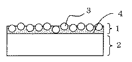
【図1】本発明の半導体モールド用離型シートの断面図である。
【符号の説明】
1 剥離層
2 基材層
3 樹脂製粒子
4 粘着剤(剥離層主成分)[0001]
TECHNICAL FIELD OF THE INVENTION
The present invention relates to a release sheet, and more particularly, to a release sheet for facilitating peeling of a semiconductor package during molding.
[0002]
[Prior art]
A semiconductor chip is usually sealed with a resin for blocking and protecting from outside air and mounted on a substrate as a molded product called a package. Conventionally, a molded product is molded as a package molded product for each chip connected via a runner which is a flow path of a sealing resin. In this case, the release is performed by a mold structure such as a protruding pin or the like, a release agent added to the sealing resin, or the like. On the other hand, in recent years, mounting of the BGA method has been used due to demands for downsizing of packages and increasing the number of pins. In this method, unlike the lead frame method where the terminals are arranged on the side of the package, the ball grid, which is the terminal, is installed on the bottom of the package, so the batch molding method that forms many packages with the sides connected to each other Can be applied. In the case of a QFN (Quad Flat Non-Leaded Package) even in the lead frame method, the lead type terminals are arranged on the bottom surface of the package, so that the collective molding method can be applied. There are two main problems in using the conventional release method in the batch molding method. One is that when using a mold structure such as a protruding pin, the versatility of the mold, which is a feature of the batch molding method, is impaired.If the package shape changes, it becomes necessary to manufacture a new mold. The problem is that a low heat shrinkable sealing material used to suppress warpage caused by an increase in the size of a molded article is difficult to sufficiently obtain releasability even by adding a release agent. Therefore, as a countermeasure, it has been practiced to mount a resin sheet in a mold to facilitate release. (For example, refer to
[0003]
[Patent Document 1]
Japanese Patent Application Laid-Open No. 2002-158242
[Problems to be solved by the invention]
An object of the present invention is to provide a method for facilitating separation of a release sheet and a package after a semiconductor package is molded.
[0005]
[Means for Solving the Problems]
The present invention relates to the following.
(1) A release sheet for a semiconductor mold, comprising a base layer and a release layer, wherein the release layer contains resin particles having an average particle diameter of 1 to 30 μm.
(2) The release sheet for a semiconductor mold according to the above (1), wherein the amount of the resin particles contained in the release layer is 0.1 to 20 parts by weight based on 100 parts by weight of the release layer.
(3) The release sheet for a semiconductor mold according to (1) or (2), wherein the main component of the resin particles is a silicone resin.
(4) The release sheet for a semiconductor mold according to (1) or (2), wherein the main component of the resin particles is an acrylic resin. (5) The above (1), wherein the main component of the resin particles is a polyethylene resin. 2) The release sheet for a semiconductor mold described in [0006]
BEST MODE FOR CARRYING OUT THE INVENTION
In order to achieve the above object, the present invention has the following configuration. That is, the present invention is a release sheet for a semiconductor mold, which is a sheet comprising a base layer and a release layer, wherein the release layer contains resin particles having an average particle diameter of 1 to 30 μm. By mounting the release layer surface of the release sheet so as to be in contact with the molded article, the sheet can be easily detached from the molded article (package) in the peeling process after molding.
As the resin particles used in the present invention, silicone particles, acrylate particles, polyethylene particles and the like are used. The average particle diameter of the resin particles is preferably 1 to 30 μm. When the average particle diameter of the particles used is smaller than 1 μm, it is difficult to sufficiently form the irregularities on the surface of the release layer, so that the effect of easily releasing the sheet from the molded package cannot be sufficiently obtained. When the average particle size of the particles used is larger than 30 μm, it is necessary to increase the thickness of the release layer in order to fix the resin particles in the release layer, which is not preferable in terms of cost. Since fixing becomes difficult, a release sheet containing resin particles cannot be stably produced. The amount of the resin particles contained in the release layer is preferably from 0.1 to 20 parts by weight based on 100 parts by weight of the release layer. If the content is less than 0.1 part by weight, it is difficult to sufficiently form irregularities on the surface of the release layer, so that it is difficult to release the sheet from the package after molding. On the other hand, if the content is more than 20 parts by weight, fixing with the release layer resin becomes difficult, and it is economically disadvantageous.
[0007]
As a main component of the release layer of the present invention, an acrylic resin or a silicone resin is used from the viewpoint of releasability from a package and heat resistance, and more preferably, a cross-linkable acrylic pressure-sensitive adhesive is used. This cross-linked acrylic pressure-sensitive adhesive has a low Tg monomer such as butyl acrylate, ethyl acrylate, and 2-ethylhexyl acrylate as a main monomer, and has a functional group such as acrylic acid, methacrylic acid, hydroxyethyl methacrylate, hydroxyethyl acrylate, acrylamide, and acrylonitrile. It is obtained by copolymerizing with a base monomer, and can be crosslinked with a crosslinking agent. Known crosslinking agents such as isocyanate-based, melamine-based, and epoxy-based crosslinking agents can be used as the crosslinking agent to be added to the acrylic copolymer. Further, as this cross-linking agent, a polyfunctional cross-linking agent such as trifunctional or tetrafunctional is more preferably used in order to form a network structure which is gradually spread in the resin.
[0008]
In the substrate layer of the present invention, from the viewpoint of heat resistance and elasticity at high temperatures, polyethylene terephthalate resin, polyethylene naphthalate resin, 6-nylon, 6,6-nylon, polyvinylidene chloride resin, 4-methylpentene, A sheet made of a syndiotactic polystyrene resin, a triacetyl cellulose resin, or the like is preferably used.
[0009]
【Example】
Hereinafter, the present invention will be described based on examples, but the scope of the present invention is not limited by these examples.
[0010]
Example 1
Mixing of 85 parts by weight: 10 parts by weight: 5 parts by weight of butyl acrylate, ethyl acrylate and 2-hydroxyethyl acrylate, using hydrogen peroxide as an initiator, and using a nonionic surfactant as an emulsifier After performing emulsion polymerization, washing with water and drying were performed to obtain an acrylic acid copolymer. Then, this copolymer was dissolved in toluene, 10 parts by weight of an isocyanate-based crosslinking agent (manufactured by Nippon Polyurethane Industry Co., Ltd., Coronate L) was used as a crosslinking agent with respect to 100 parts by weight of the solid content of this solution, and the average particle diameter was 2 μm as resin particles. 5 parts by weight of silicone particles (Toray Dow Corning, Trefil E-600) were added to prepare a varnish. This was applied to a biaxially stretched modified polyethylene terephthalate sheet (S-38 manufactured by Unitika) so as to have a solid content of 5 μm in thickness, and dried by heating at 100 ° C. for 3 minutes to obtain a release sheet. The sheet was mounted on an upper mold of a transfer mold and subjected to transfer molding, and then the releasability between the molded product and the sheet was observed. The results are shown in Table 1.
[0011]
Example 2
A release sheet was prepared in the same manner as in Example 1, except that 5 parts by weight of acrylic resin particles (manufactured by Soken Chemical Co., Ltd., MR-20G) having an average particle diameter of 20 μm were used as the resin particles to be added. The results are shown in Table 1.
[0012]
Example 3
A release sheet was prepared in the same manner as in Example 1 except that 5 parts by weight of polyethylene resin particles having an average particle diameter of 15 μm (manufactured by Sumitomo Seika Co., Ltd., Flowsen UF-1.5) were used as the resin particles to be added. Table 1 shows the results.
[0013]
Comparative Example 1
A release sheet was prepared in the same manner as in Example 1 except that no resin particles were added to the varnish in Example 1, and the results are shown in Table 1.
[0014]
Comparative Example 2
A release sheet was prepared in the same manner as in Example 1 except that 5 parts by weight of acrylic resin particles (Staphyroid IM-601, manufactured by Takeda Pharmaceutical Co., Ltd.) having an average particle diameter of 0.3 μm were used as the resin particles to be added. The results are shown in Table 1.
[0015]
Comparative Example 3
A release sheet was prepared in the same manner as in Example 1, except that 0.01 parts by weight of silicone resin particles (Toray Dow Corning, Trefil E-600) having an average particle diameter of 2 μm were used as the resin particles to be added. Table 1 shows the results.
[0016]
[Table 1]
X: The peeling layer has adhered by visual observation.
[0017]
【The invention's effect】
The following effects can be expected by using the release sheet of the present invention at the time of manufacturing a semiconductor package. That is, it is possible to prevent a peeling trouble (a temporary stop of a line due to difficulty in peeling, a decrease in production tact, etc.) in a peeling step of the package and the release sheet, and it is possible to improve a production efficiency of a non-defective package.
[Brief description of the drawings]
FIG. 1 is a cross-sectional view of a release sheet for a semiconductor mold of the present invention.
[Explanation of symbols]
REFERENCE SIGNS
Claims (5)
Priority Applications (1)
| Application Number | Priority Date | Filing Date | Title |
|---|---|---|---|
| JP2002368100A JP2004200467A (en) | 2002-12-19 | 2002-12-19 | Release sheet for semiconductor mould |
Applications Claiming Priority (1)
| Application Number | Priority Date | Filing Date | Title |
|---|---|---|---|
| JP2002368100A JP2004200467A (en) | 2002-12-19 | 2002-12-19 | Release sheet for semiconductor mould |
Publications (1)
| Publication Number | Publication Date |
|---|---|
| JP2004200467A true JP2004200467A (en) | 2004-07-15 |
Family
ID=32764776
Family Applications (1)
| Application Number | Title | Priority Date | Filing Date |
|---|---|---|---|
| JP2002368100A Pending JP2004200467A (en) | 2002-12-19 | 2002-12-19 | Release sheet for semiconductor mould |
Country Status (1)
| Country | Link |
|---|---|
| JP (1) | JP2004200467A (en) |
Cited By (12)
| Publication number | Priority date | Publication date | Assignee | Title |
|---|---|---|---|---|
| JP2014063971A (en) * | 2012-09-21 | 2014-04-10 | Toray Advanced Materials Korea Inc | Adhesive composition for masking tape in mold underfill process, and masking tape using the same |
| CN104112693A (en) * | 2013-04-19 | 2014-10-22 | 株式会社巴川制纸所 | Release film for mold forming |
| JP2016092272A (en) * | 2014-11-06 | 2016-05-23 | 日立化成株式会社 | Release sheet for semiconductor compression molding, and semiconductor package molded by use thereof |
| JP2016192433A (en) * | 2015-03-30 | 2016-11-10 | 株式会社巴川製紙所 | Process sheet for manufacturing semiconductor device |
| JP2016192503A (en) * | 2015-03-31 | 2016-11-10 | 株式会社巴川製紙所 | Process sheet for semiconductor device manufacturing |
| WO2017200102A1 (en) * | 2016-05-20 | 2017-11-23 | 日立化成株式会社 | Mold release film |
| JP2018037558A (en) * | 2016-08-31 | 2018-03-08 | 富士フイルム株式会社 | Method for manufacturing laminate, composition for temporary adhesion, and temporary adhesive film |
| CN109155257A (en) * | 2016-05-20 | 2019-01-04 | 日立化成株式会社 | Semiconductor compression forming release sheet and the semiconductor packages being molded with using it |
| JP2019029423A (en) * | 2017-07-26 | 2019-02-21 | リンテック株式会社 | Release film |
| JP2019153804A (en) * | 2019-04-26 | 2019-09-12 | 日立化成株式会社 | Release sheet for semiconductor compression molding, and semiconductor package molded by use thereof |
| TWI697406B (en) * | 2016-05-20 | 2020-07-01 | 日商日立化成股份有限公司 | Release sheet for compression molding of a semiconductor, and semiconductor package molded using the same |
| JP2021061437A (en) * | 2021-01-04 | 2021-04-15 | 昭和電工マテリアルズ株式会社 | Release sheet for semiconductor compression molding, and semiconductor package molded by use thereof |
-
2002
- 2002-12-19 JP JP2002368100A patent/JP2004200467A/en active Pending
Cited By (19)
| Publication number | Priority date | Publication date | Assignee | Title |
|---|---|---|---|---|
| JP2014063971A (en) * | 2012-09-21 | 2014-04-10 | Toray Advanced Materials Korea Inc | Adhesive composition for masking tape in mold underfill process, and masking tape using the same |
| CN104112693A (en) * | 2013-04-19 | 2014-10-22 | 株式会社巴川制纸所 | Release film for mold forming |
| JP2014212239A (en) * | 2013-04-19 | 2014-11-13 | 株式会社巴川製紙所 | Release sheet for molding |
| JP2016092272A (en) * | 2014-11-06 | 2016-05-23 | 日立化成株式会社 | Release sheet for semiconductor compression molding, and semiconductor package molded by use thereof |
| JP2016192433A (en) * | 2015-03-30 | 2016-11-10 | 株式会社巴川製紙所 | Process sheet for manufacturing semiconductor device |
| JP2016192503A (en) * | 2015-03-31 | 2016-11-10 | 株式会社巴川製紙所 | Process sheet for semiconductor device manufacturing |
| JPWO2017200102A1 (en) * | 2016-05-20 | 2018-05-31 | 日立化成株式会社 | Release film |
| WO2017200102A1 (en) * | 2016-05-20 | 2017-11-23 | 日立化成株式会社 | Mold release film |
| CN109153155A (en) * | 2016-05-20 | 2019-01-04 | 日立化成株式会社 | Mold release film |
| CN109155257A (en) * | 2016-05-20 | 2019-01-04 | 日立化成株式会社 | Semiconductor compression forming release sheet and the semiconductor packages being molded with using it |
| JPWO2017199440A1 (en) * | 2016-05-20 | 2019-04-04 | 日立化成株式会社 | Release sheet for semiconductor compression molding and semiconductor package molded using the same |
| TWI697406B (en) * | 2016-05-20 | 2020-07-01 | 日商日立化成股份有限公司 | Release sheet for compression molding of a semiconductor, and semiconductor package molded using the same |
| CN109153155B (en) * | 2016-05-20 | 2020-11-10 | 昭和电工材料株式会社 | release film |
| CN109155257B (en) * | 2016-05-20 | 2023-09-15 | 株式会社力森诺科 | Release sheet for semiconductor compression molding and semiconductor package molded using the same |
| JP2018037558A (en) * | 2016-08-31 | 2018-03-08 | 富士フイルム株式会社 | Method for manufacturing laminate, composition for temporary adhesion, and temporary adhesive film |
| JP2019029423A (en) * | 2017-07-26 | 2019-02-21 | リンテック株式会社 | Release film |
| JP2019153804A (en) * | 2019-04-26 | 2019-09-12 | 日立化成株式会社 | Release sheet for semiconductor compression molding, and semiconductor package molded by use thereof |
| JP2021061437A (en) * | 2021-01-04 | 2021-04-15 | 昭和電工マテリアルズ株式会社 | Release sheet for semiconductor compression molding, and semiconductor package molded by use thereof |
| JP7052891B2 (en) | 2021-01-04 | 2022-04-12 | 昭和電工マテリアルズ株式会社 | Release sheet for semiconductor compression molding and semiconductor package molded using this |
Similar Documents
| Publication | Publication Date | Title |
|---|---|---|
| JP5718005B2 (en) | A heat-resistant adhesive tape for manufacturing a semiconductor device and a method for manufacturing a semiconductor device using the tape. | |
| JP2004200467A (en) | Release sheet for semiconductor mould | |
| JP5552404B2 (en) | A heat-resistant adhesive tape for manufacturing a semiconductor device and a method for manufacturing a semiconductor device using the tape. | |
| JP6414345B2 (en) | Release film | |
| CN1320619C (en) | Method for producing semiconductor and heat-resisting pressure-sensitive adhesive tape | |
| TW201900801A (en) | Temporary protective film for semiconductor sealing molding | |
| KR20060056362A (en) | Heat resistant masking tape | |
| CN103305140A (en) | Heat-resistance pressure-sensitive adhesive tape for semiconductor device production and method for producing semiconductor device by using heat-resistance pressure-sensitive adhesive tape | |
| US20130244377A1 (en) | Heat-resistant pressure-sensitive adhesive tape for production of semiconductor device and method for producing semiconductor device using the tape | |
| US20190275763A1 (en) | Mold release sheet for semiconductor compression molding and semiconductor package which is molded using same | |
| CN112055734B (en) | Adhesive tape and method for manufacturing semiconductor device using the same | |
| JP7593326B2 (en) | Release film and method for manufacturing semiconductor package | |
| JP6547408B2 (en) | Method for producing ground substrate, and film-like pressure-sensitive adhesive and laminate used therefor | |
| JP5659408B2 (en) | Adhesive masking tape for mold underfill process of die exposed flip chip package (DEFCP) | |
| TWI759029B (en) | Adhesive tape | |
| JP7052891B2 (en) | Release sheet for semiconductor compression molding and semiconductor package molded using this | |
| JP4096659B2 (en) | Release sheet for semiconductor package and manufacturing method of resin-encapsulated semiconductor device | |
| JP2004074713A (en) | Release sheet for semiconductor mold | |
| JP2003313518A (en) | Heat resistant adhesive tape | |
| CN103305139A (en) | Heat-resistance pressure-sensitive adhesive tape for semiconductor device production and method for producing semiconductor device by using heat-resistance pressure-sensitive adhesive tape | |
| JP5160575B2 (en) | Semiconductor device manufacturing method and heat-resistant adhesive tape used therefor | |
| KR102960522B1 (en) | Method for manufacturing release film and semiconductor package | |
| TWI697406B (en) | Release sheet for compression molding of a semiconductor, and semiconductor package molded using the same | |
| JP7815867B2 (en) | Release film for semiconductor molding and method for manufacturing semiconductor device | |
| JP4086322B2 (en) | Thermally conductive pressure sensitive adhesive and its adhesive sheets |
Legal Events
| Date | Code | Title | Description |
|---|---|---|---|
| A621 | Written request for application examination |
Free format text: JAPANESE INTERMEDIATE CODE: A621 Effective date: 20051202 |
|
| A977 | Report on retrieval |
Free format text: JAPANESE INTERMEDIATE CODE: A971007 Effective date: 20071004 |
|
| A131 | Notification of reasons for refusal |
Free format text: JAPANESE INTERMEDIATE CODE: A131 Effective date: 20071009 |
|
| A02 | Decision of refusal |
Free format text: JAPANESE INTERMEDIATE CODE: A02 Effective date: 20080228 |