JP2004200680A - 検査方法およびデバイス製造方法 - Google Patents
検査方法およびデバイス製造方法 Download PDFInfo
- Publication number
- JP2004200680A JP2004200680A JP2003408154A JP2003408154A JP2004200680A JP 2004200680 A JP2004200680 A JP 2004200680A JP 2003408154 A JP2003408154 A JP 2003408154A JP 2003408154 A JP2003408154 A JP 2003408154A JP 2004200680 A JP2004200680 A JP 2004200680A
- Authority
- JP
- Japan
- Prior art keywords
- aberration
- test pattern
- lithographic apparatus
- inspection method
- radiation
- Prior art date
- Legal status (The legal status is an assumption and is not a legal conclusion. Google has not performed a legal analysis and makes no representation as to the accuracy of the status listed.)
- Granted
Links
Images


Classifications
-
- G—PHYSICS
- G03—PHOTOGRAPHY; CINEMATOGRAPHY; ANALOGOUS TECHNIQUES USING WAVES OTHER THAN OPTICAL WAVES; ELECTROGRAPHY; HOLOGRAPHY
- G03F—PHOTOMECHANICAL PRODUCTION OF TEXTURED OR PATTERNED SURFACES, e.g. FOR PRINTING, FOR PROCESSING OF SEMICONDUCTOR DEVICES; MATERIALS THEREFOR; ORIGINALS THEREFOR; APPARATUS SPECIALLY ADAPTED THEREFOR
- G03F7/00—Photomechanical, e.g. photolithographic, production of textured or patterned surfaces, e.g. printing surfaces; Materials therefor, e.g. comprising photoresists; Apparatus specially adapted therefor
- G03F7/70—Microphotolithographic exposure; Apparatus therefor
- G03F7/70483—Information management; Active and passive control; Testing; Wafer monitoring, e.g. pattern monitoring
- G03F7/70591—Testing optical components
- G03F7/706—Aberration measurement
-
- H—ELECTRICITY
- H10—SEMICONDUCTOR DEVICES; ELECTRIC SOLID-STATE DEVICES NOT OTHERWISE PROVIDED FOR
- H10P—GENERIC PROCESSES OR APPARATUS FOR THE MANUFACTURE OR TREATMENT OF DEVICES COVERED BY CLASS H10
- H10P76/00—Manufacture or treatment of masks on semiconductor bodies, e.g. by lithography or photolithography
Landscapes
- Physics & Mathematics (AREA)
- General Physics & Mathematics (AREA)
- Exposure And Positioning Against Photoresist Photosensitive Materials (AREA)
- Testing Of Optical Devices Or Fibers (AREA)
- Exposure Of Semiconductors, Excluding Electron Or Ion Beam Exposure (AREA)
Abstract
【解決手段】検査方法は、少なくとも多少の対称性を有し、装置における特定の収差に感応するテスト・パターン基板に焼き付け、スキャテロメータを使用してその収差に関する情報を導き出すことで、リトグラフの収差を検出する。テスト構造には二本棒格子が含まれ、これによればコマ収差を示す情報を導き出すために、内側および外側の衝撃係数を再現することができる。これに代えて、六角形配列構造を使用することもでき、この場合にはスキャテロメトリ・データは三波収差を示す点の直径を再現するために使用できる。
【選択図】図4
Description
放射装置を使用して放射光の投影ビームを形成する段階と、
断面にパターンを有する投影ビームを与えるために、パターン形成手段を使用する段階と、
放射光感応物質の層の対象箇所上に放射光のパターン形成したビームを投影する段階とを含むデバイス製造方法において、
前記パターンが、処理層を表すパターンと、少なくとも一つの対称性を有するテスト・パターンとを含み、テスト・パターンが、リトグラフ装置に存在し得る少なくとも1つの他の種類の収差に感応し、また、
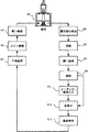
スキャテロメータを使用して前記テスト・パターンの反射スペクトルを測定する段階と、
前記反射スペクトルから、前記リトグラフ装置に存在する前記少なくとも一つの種類の収差の大きさを示す情報を導き出す段階とをさらに含むことを特徴とするデバイス製造方法が提供される。
図面において、同じ符号は同じ部分を示す。
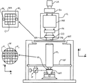
図1は本発明による方法で使用できるリトグラフ投影装置を模式的に示している。この装置は、
放射光(例えばDUV放射光)の投影ビームPBを供給する放射装置Ex,ILであって、特別の場合には放射光源LAも含む放射装置Ex,ILと、
マスクMA(例えばレチクル)を保持するマスク保持具を備え、部材PLに対してマスクを正確に位置決めするための第一の位置決め手段に連結された第一の物品テーブル(マスク・テーブル)MTと、
基板W(例えばレジスト被覆シリコン・ウェーハ)を保持する基板保持具を備え、部材PLに対して基板を正確に位置決めするための第二の位置決め手段に連結された第二の物品テーブル(基板テーブル)WTと、
基板Wの対象箇所C(例えば一以上のダイスを含む)にマスクMAの照射部分を像形成する投影装置(「レンズ」)PL(例えば屈折式レンズ装置)とを含む。
1.ステップ態様では、マスク・テーブルMTおよび基板テーブルWTは基本的に静止状態に保持される一方、投影ビームに与えられた全パターンが一回の移動(すなわち一回の静止露光)で対象箇所Cに投影される。基板テーブルWTはその後にXおよび/またはY方向へ移動され、異なる対象箇所Cが露光できるようにされる。ステップ態様では、露光領域の最大寸法が、一回の静止露光で像形成される対象箇所Cの寸法を制限する。
前記の使用態様の組合せおよび/または変形例、または全く異なる使用態様も使用することができる。
S1 −S2 = 0 (1)
w1 ’= w1 + w
w2 ’= w2 − w (2)
S1 −S2 = 2dS/dW × Δw (3)
dS/dW = (S3 −S2 )/d (4)
Δw = ((S1 −S2 )/(S3 −S2 )) × d/2 (5)
Claims (10)
- リトグラフ装置を使用して、該リトグラフ装置に存在し得る少なくとも1種類の収差に感応し、少なくとも1つの対称性を有するテスト・パターンを基板に焼き付ける段階と、
スキャテロメータを使用して、前記テスト・パターンの反射スペクトルを測定する段階と、
前記反射スペクトルから、前記リトグラフ装置に存在する前記少なくとも1種類の収差の大きさを示す情報を導き出す段階とを含む検査方法。 - 前記テスト・パターンが二本棒格子を含む請求項1に記載された検査方法。
- 前記収差の大きさを示す情報を導き出す段階が、前記リトグラフ装置のコマ収差を示す情報を導き出すために、パラメータとして内側および外側の衝撃係数を有する二本棒格子を再現する段階を含む請求項2に記載された検査方法。
- 前記テスト・パターンが六角形の点配列を含む請求項1から請求項3までのいずれか1項に記載された検査方法。
- 前記収差の大きさを示す情報を導き出す段階が、スポット直径を再現する段階を含み、配列の各単位セルにおける前記スポット直径の差がリトグラフ装置の三波収差を示す請求項4に記載された検査方法。
- 前記テスト・パターンが、同じ基本的対称形状の第一、第二および第三の構造を含み、前記第一および第二の構造が、同一であるが反対方向の前記基本的対称形状からの非対称の偏りを有しており、前記第三の構造は前記第二の構造に比較して付加された非対称の偏りを有している請求項1に記載された検査方法。
- 前記収差の大きさを示す情報を導き出す段階が、前記第一および第二の構造から得たスキャテロメトリ信号の差を、前記第三および第二の構造から得たスキャテロメトリ信号の差で割る段階を含む請求項6に記載された検査方法。
- 前記第一、第二および第三の構造が二本棒格子であり、前記第一の構造は棒部の幅w1および w2 を有し、w1 はw2 よりも大きく、前記第二の構造は前記第一の構造の鏡像であり、また第三の構造はw1 −w2 よりも小さいdで加算および減算した棒部の幅w2 +dおよびw1 −dを有している請求項7または請求項8に記載された検査方法。
- 前記スキャテロメータが垂直入射スキャテロメータである請求項1から請求項8までのいずれか1項に記載された検査方法。
- 放射光感応物質の層で少なくとも部分的に覆われた基板を形成する段階と、
放射装置を使用して放射光の投影ビームを形成する段階と、
断面にパターンを有する投影ビームを与えるためにパターン形成手段を使用する段階と、
放射光感応物質の層の対象部分にパターン形成した放射光のビームを投影する段階とを含むデバイス製造方法において、
前記パターンが、処理層を表すパターンと、少なくとも一つの対称性を有するテスト・パターンとを含み、該テスト・パターンが、リトグラフ装置に存在し得る少なくとも一つの他の種類の収差に感応し、また
スキャテロメータを使用して前記テスト・パターンの反射スペクトルを測定する段階と、
前記反射スペクトルから、前記リトグラフ装置に存在する前記少なくとも一つの種類の収差の大きさを示す情報を導き出す段階とをさらに含むことを特徴とするデバイス製造方法。
Applications Claiming Priority (1)
| Application Number | Priority Date | Filing Date | Title |
|---|---|---|---|
| EP02257609 | 2002-11-01 |
Publications (2)
| Publication Number | Publication Date |
|---|---|
| JP2004200680A true JP2004200680A (ja) | 2004-07-15 |
| JP3981664B2 JP3981664B2 (ja) | 2007-09-26 |
Family
ID=32479814
Family Applications (1)
| Application Number | Title | Priority Date | Filing Date |
|---|---|---|---|
| JP2003408154A Expired - Fee Related JP3981664B2 (ja) | 2002-11-01 | 2003-10-31 | 検査方法およびデバイス製造方法 |
Country Status (6)
| Country | Link |
|---|---|
| US (2) | US7151594B2 (ja) |
| JP (1) | JP3981664B2 (ja) |
| KR (1) | KR100592583B1 (ja) |
| CN (1) | CN100568099C (ja) |
| SG (1) | SG125926A1 (ja) |
| TW (1) | TWI237742B (ja) |
Cited By (6)
| Publication number | Priority date | Publication date | Assignee | Title |
|---|---|---|---|---|
| WO2006054496A1 (ja) * | 2004-11-16 | 2006-05-26 | Tokyo Electron Limited | 同期精度検出方法およびシステム、収差検出方法およびシステム、ならびにコンピュータプログラム |
| WO2007029828A1 (ja) * | 2005-09-09 | 2007-03-15 | Nikon Corporation | 解析方法、露光方法及びデバイス製造方法 |
| JP2007305971A (ja) * | 2006-03-27 | 2007-11-22 | Jordan Valley Semiconductors Ltd | X線を用いるオーバレイ計測 |
| JP2008098636A (ja) * | 2006-10-13 | 2008-04-24 | Asml Netherlands Bv | 検査方法および装置、リソグラフィ装置、リソグラフィ処理セルおよびデバイス製造方法 |
| JP2008311645A (ja) * | 2007-06-13 | 2008-12-25 | Asml Netherlands Bv | インスペクション方法および装置、リソグラフィ装置、リソグラフィ処理セル、ならびにデバイス製造方法 |
| US8111374B2 (en) | 2005-09-09 | 2012-02-07 | Nikon Corporation | Analysis method, exposure method, and device manufacturing method |
Families Citing this family (16)
| Publication number | Priority date | Publication date | Assignee | Title |
|---|---|---|---|---|
| US7352453B2 (en) * | 2003-01-17 | 2008-04-01 | Kla-Tencor Technologies Corporation | Method for process optimization and control by comparison between 2 or more measured scatterometry signals |
| EP1612605A1 (de) * | 2004-07-03 | 2006-01-04 | Technomedica AG | Laserbelichtung |
| US20070002336A1 (en) * | 2005-06-30 | 2007-01-04 | Asml Netherlands B.V. | Metrology apparatus, lithographic apparatus, process apparatus, metrology method and device manufacturing method |
| US7532307B2 (en) * | 2005-06-30 | 2009-05-12 | Asml Netherlands B.V. | Focus determination method, device manufacturing method, and mask |
| US7916284B2 (en) * | 2006-07-18 | 2011-03-29 | Asml Netherlands B.V. | Inspection method and apparatus, lithographic apparatus, lithographic processing cell and device manufacturing method |
| US7892442B2 (en) * | 2007-03-08 | 2011-02-22 | Tdk Corporation | Method of manufacturing a thin-film magnetic head, thin-film magnetic head manufacturing apparatus, and thin-film magnetic head manufacturing system |
| US7716003B1 (en) | 2007-07-16 | 2010-05-11 | Kla-Tencor Technologies Corporation | Model-based measurement of semiconductor device features with feed forward use of data for dimensionality reduction |
| US7826072B1 (en) | 2007-08-16 | 2010-11-02 | Kla-Tencor Technologies Corporation | Method for optimizing the configuration of a scatterometry measurement system |
| NL1036597A1 (nl) * | 2008-02-29 | 2009-09-01 | Asml Netherlands Bv | Metrology method and apparatus, lithographic apparatus, and device manufacturing method. |
| WO2010049348A2 (en) * | 2008-10-31 | 2010-05-06 | Asml Netherlands B.V. | Inspection method and apparatus, lithographic apparatus, lithographic processing cell and device manufacturing method for determining a property of a substrate |
| SG172294A1 (en) | 2008-12-30 | 2011-07-28 | Asml Netherlands Bv | Inspection method and apparatus, lithographic apparatus, lithographic processing cell and device manufacturing method |
| FR2942070B1 (fr) * | 2009-02-11 | 2011-03-11 | Commissariat Energie Atomique | Procede de correction d'astigmatisme en imagerie par spectromicroscopie a emission d'electrons |
| EP2430498B1 (en) * | 2009-05-12 | 2018-01-31 | ASML Netherlands BV | Inspection method for lithography |
| JP5391055B2 (ja) * | 2009-12-25 | 2014-01-15 | 東京エレクトロン株式会社 | 半導体装置の製造方法及び半導体装置の製造システム |
| WO2017108395A1 (en) | 2015-12-21 | 2017-06-29 | Asml Netherlands B.V. | Methods and patterning devices and apparatuses for measuring focus performance of a lithographic apparatus, device manufacturing method |
| JP6808684B2 (ja) * | 2018-06-14 | 2021-01-06 | キヤノン株式会社 | 情報処理装置、判定方法、プログラム、リソグラフィシステム、および物品の製造方法 |
Citations (6)
| Publication number | Priority date | Publication date | Assignee | Title |
|---|---|---|---|---|
| JP2002131185A (ja) * | 2000-10-20 | 2002-05-09 | Nec Corp | コマ収差の測定用マスク及びコマ収差の測定方法 |
| JP2002198303A (ja) * | 2000-12-27 | 2002-07-12 | Nikon Corp | 露光装置、光学特性計測方法、及びデバイス製造方法 |
| WO2002070985A1 (en) * | 2001-03-02 | 2002-09-12 | Accent Optical Technologies, Inc. | Line profile asymmetry measurement using scatterometry |
| JP2002260994A (ja) * | 2001-03-05 | 2002-09-13 | Tokyo Electron Ltd | 基板処理装置 |
| JP2002311564A (ja) * | 2001-01-29 | 2002-10-23 | Tanbaa Technologies Inc | 散乱測定を用いてマスクルールを求めるための方法および装置 |
| JP2005513757A (ja) * | 2001-06-26 | 2005-05-12 | ケーエルエー−テンカー・コーポレーション | リソグラフィのフォーカスおよび露光を決定する方法 |
Family Cites Families (8)
| Publication number | Priority date | Publication date | Assignee | Title |
|---|---|---|---|---|
| EP0985977A1 (en) | 1998-09-11 | 2000-03-15 | Lucent Technologies Inc. | Integrated circuit device fabrication utilizing latent imagery |
| JP3801809B2 (ja) * | 1999-04-27 | 2006-07-26 | 株式会社ジェイテクト | 軸とヨークの結合構造 |
| US6429930B1 (en) * | 2000-09-06 | 2002-08-06 | Accent Optical Technologies, Inc. | Determination of center of focus by diffraction signature analysis |
| US6819426B2 (en) | 2001-02-12 | 2004-11-16 | Therma-Wave, Inc. | Overlay alignment metrology using diffraction gratings |
| US6650422B2 (en) | 2001-03-26 | 2003-11-18 | Advanced Micro Devices, Inc. | Scatterometry techniques to ascertain asymmetry profile of features and generate a feedback or feedforward process control data associated therewith |
| US7382447B2 (en) * | 2001-06-26 | 2008-06-03 | Kla-Tencor Technologies Corporation | Method for determining lithographic focus and exposure |
| WO2003001297A2 (en) | 2001-06-26 | 2003-01-03 | Kla-Tencor Corporation | Method for determining lithographic focus and exposure |
| US6458605B1 (en) * | 2001-06-28 | 2002-10-01 | Advanced Micro Devices, Inc. | Method and apparatus for controlling photolithography overlay registration |
-
2003
- 2003-10-30 SG SG200306440A patent/SG125926A1/en unknown
- 2003-10-30 US US10/696,742 patent/US7151594B2/en not_active Expired - Lifetime
- 2003-10-31 JP JP2003408154A patent/JP3981664B2/ja not_active Expired - Fee Related
- 2003-10-31 KR KR1020030077068A patent/KR100592583B1/ko not_active Expired - Fee Related
- 2003-10-31 TW TW092130516A patent/TWI237742B/zh not_active IP Right Cessation
- 2003-11-01 CN CNB2003101203429A patent/CN100568099C/zh not_active Expired - Fee Related
-
2006
- 2006-11-08 US US11/594,075 patent/US7312860B2/en not_active Expired - Lifetime
Patent Citations (6)
| Publication number | Priority date | Publication date | Assignee | Title |
|---|---|---|---|---|
| JP2002131185A (ja) * | 2000-10-20 | 2002-05-09 | Nec Corp | コマ収差の測定用マスク及びコマ収差の測定方法 |
| JP2002198303A (ja) * | 2000-12-27 | 2002-07-12 | Nikon Corp | 露光装置、光学特性計測方法、及びデバイス製造方法 |
| JP2002311564A (ja) * | 2001-01-29 | 2002-10-23 | Tanbaa Technologies Inc | 散乱測定を用いてマスクルールを求めるための方法および装置 |
| WO2002070985A1 (en) * | 2001-03-02 | 2002-09-12 | Accent Optical Technologies, Inc. | Line profile asymmetry measurement using scatterometry |
| JP2002260994A (ja) * | 2001-03-05 | 2002-09-13 | Tokyo Electron Ltd | 基板処理装置 |
| JP2005513757A (ja) * | 2001-06-26 | 2005-05-12 | ケーエルエー−テンカー・コーポレーション | リソグラフィのフォーカスおよび露光を決定する方法 |
Cited By (9)
| Publication number | Priority date | Publication date | Assignee | Title |
|---|---|---|---|---|
| WO2006054496A1 (ja) * | 2004-11-16 | 2006-05-26 | Tokyo Electron Limited | 同期精度検出方法およびシステム、収差検出方法およびシステム、ならびにコンピュータプログラム |
| WO2007029828A1 (ja) * | 2005-09-09 | 2007-03-15 | Nikon Corporation | 解析方法、露光方法及びデバイス製造方法 |
| US8111374B2 (en) | 2005-09-09 | 2012-02-07 | Nikon Corporation | Analysis method, exposure method, and device manufacturing method |
| JP4992718B2 (ja) * | 2005-09-09 | 2012-08-08 | 株式会社ニコン | 解析方法、露光方法及びデバイス製造方法 |
| JP2007305971A (ja) * | 2006-03-27 | 2007-11-22 | Jordan Valley Semiconductors Ltd | X線を用いるオーバレイ計測 |
| JP2008098636A (ja) * | 2006-10-13 | 2008-04-24 | Asml Netherlands Bv | 検査方法および装置、リソグラフィ装置、リソグラフィ処理セルおよびデバイス製造方法 |
| US8294907B2 (en) | 2006-10-13 | 2012-10-23 | Asml Netherlands B.V. | Inspection method and apparatus, lithographic apparatus, lithographic processing cell and device manufacturing method |
| JP2008311645A (ja) * | 2007-06-13 | 2008-12-25 | Asml Netherlands Bv | インスペクション方法および装置、リソグラフィ装置、リソグラフィ処理セル、ならびにデバイス製造方法 |
| US7911612B2 (en) | 2007-06-13 | 2011-03-22 | Asml Netherlands B.V. | Inspection method and apparatus, lithographic apparatus, lithographic processing cell and device manufacturing method |
Also Published As
| Publication number | Publication date |
|---|---|
| KR20040038884A (ko) | 2004-05-08 |
| TW200424786A (en) | 2004-11-16 |
| US20070052948A1 (en) | 2007-03-08 |
| US7312860B2 (en) | 2007-12-25 |
| US20040114132A1 (en) | 2004-06-17 |
| JP3981664B2 (ja) | 2007-09-26 |
| US7151594B2 (en) | 2006-12-19 |
| CN1499292A (zh) | 2004-05-26 |
| SG125926A1 (en) | 2006-10-30 |
| KR100592583B1 (ko) | 2006-06-26 |
| CN100568099C (zh) | 2009-12-09 |
| TWI237742B (en) | 2005-08-11 |
Similar Documents
| Publication | Publication Date | Title |
|---|---|---|
| JP3972035B2 (ja) | 検査方法とデバイス製造方法 | |
| JP3981664B2 (ja) | 検査方法およびデバイス製造方法 | |
| JP5412528B2 (ja) | 検査方法、検査システム、基板、およびマスク | |
| JP5100887B2 (ja) | 基板のモデルを評価する方法 | |
| JP4912241B2 (ja) | インスペクション方法およびインスペクション装置、リソグラフィ装置、リソグラフィ処理セルならびにデバイス製造方法 | |
| JP5288808B2 (ja) | 測定方法、検査装置およびリソグラフィ装置 | |
| KR101037411B1 (ko) | 메트롤로지 툴을 캘리브레이션하는데 사용하기 위한 기판을 형성하는 방법, 캘리브레이션 기판 및 메트롤로지 툴 캘리브레이션 방법 | |
| JP4812712B2 (ja) | 基板の特性を測定する方法及びデバイス測定方法 | |
| US9798250B2 (en) | Lithographic apparatus for measuring overlay error and a device manufacturing method | |
| JP4578495B2 (ja) | オーバーレイ測定品質表示を使用するリソグラフィ装置およびデバイス製造方法 | |
| JP4861363B2 (ja) | 角度分解スキャトロメータおよび検査方法 | |
| JP2008042200A (ja) | 角度分解分光リソグラフィの特徴付けのための方法および装置 | |
| JP2003022968A (ja) | リソグラフィ装置の較正方法、リソグラフィ装置の較正に使用するマスク、リソグラフィ装置、デバイス製造方法、該デバイス製造方法により製造されたデバイス | |
| US7177010B2 (en) | Lithographic apparatus and device manufacturing method | |
| JP2009081436A (ja) | オーバレイエラーの測定方法、検査装置及びリソグラフィ装置 | |
| US20100328636A1 (en) | Producing a Marker Pattern and Measurement of an Exposure-Related Property of an Exposure Apparatus | |
| NL2005044A (en) | Inspection method and apparatus, lithographic apparatus, lithographic processing cell and device manufacturing method. | |
| JP5204062B2 (ja) | 球状色収差を補正する半導体検査装置、及び球状色収差の補正方法 | |
| US20100227280A1 (en) | Method of Measuring a Characteristic | |
| US20100315613A1 (en) | Inspection Method and Apparatus, Lithographic Apparatus, Lithographic Processing Cell and Device Manufacturing Method | |
| EP1416328A2 (en) | Inspection method and device manufacturing method |
Legal Events
| Date | Code | Title | Description |
|---|---|---|---|
| RD03 | Notification of appointment of power of attorney |
Free format text: JAPANESE INTERMEDIATE CODE: A7423 Effective date: 20060904 |
|
| A977 | Report on retrieval |
Free format text: JAPANESE INTERMEDIATE CODE: A971007 Effective date: 20061019 |
|
| A131 | Notification of reasons for refusal |
Free format text: JAPANESE INTERMEDIATE CODE: A131 Effective date: 20061023 |
|
| A521 | Request for written amendment filed |
Free format text: JAPANESE INTERMEDIATE CODE: A523 Effective date: 20070123 |
|
| RD05 | Notification of revocation of power of attorney |
Free format text: JAPANESE INTERMEDIATE CODE: A7425 Effective date: 20070314 |
|
| A521 | Request for written amendment filed |
Free format text: JAPANESE INTERMEDIATE CODE: A523 Effective date: 20070515 |
|
| TRDD | Decision of grant or rejection written | ||
| A01 | Written decision to grant a patent or to grant a registration (utility model) |
Free format text: JAPANESE INTERMEDIATE CODE: A01 Effective date: 20070613 |
|
| A61 | First payment of annual fees (during grant procedure) |
Free format text: JAPANESE INTERMEDIATE CODE: A61 Effective date: 20070702 |
|
| R150 | Certificate of patent or registration of utility model |
Free format text: JAPANESE INTERMEDIATE CODE: R150 |
|
| FPAY | Renewal fee payment (event date is renewal date of database) |
Free format text: PAYMENT UNTIL: 20100706 Year of fee payment: 3 |
|
| FPAY | Renewal fee payment (event date is renewal date of database) |
Free format text: PAYMENT UNTIL: 20110706 Year of fee payment: 4 |
|
| FPAY | Renewal fee payment (event date is renewal date of database) |
Free format text: PAYMENT UNTIL: 20110706 Year of fee payment: 4 |
|
| FPAY | Renewal fee payment (event date is renewal date of database) |
Free format text: PAYMENT UNTIL: 20120706 Year of fee payment: 5 |
|
| FPAY | Renewal fee payment (event date is renewal date of database) |
Free format text: PAYMENT UNTIL: 20120706 Year of fee payment: 5 |
|
| FPAY | Renewal fee payment (event date is renewal date of database) |
Free format text: PAYMENT UNTIL: 20130706 Year of fee payment: 6 |
|
| LAPS | Cancellation because of no payment of annual fees |