JP2004200914A - Piezoelectric device, mobile phone device and electronic device using piezoelectric device - Google Patents
Piezoelectric device, mobile phone device and electronic device using piezoelectric device Download PDFInfo
- Publication number
- JP2004200914A JP2004200914A JP2002365528A JP2002365528A JP2004200914A JP 2004200914 A JP2004200914 A JP 2004200914A JP 2002365528 A JP2002365528 A JP 2002365528A JP 2002365528 A JP2002365528 A JP 2002365528A JP 2004200914 A JP2004200914 A JP 2004200914A
- Authority
- JP
- Japan
- Prior art keywords
- piezoelectric
- base
- vibrating
- hole
- piezoelectric device
- Prior art date
- Legal status (The legal status is an assumption and is not a legal conclusion. Google has not performed a legal analysis and makes no representation as to the accuracy of the status listed.)
- Withdrawn
Links
- 239000000853 adhesive Substances 0.000 claims abstract description 56
- 230000001070 adhesive effect Effects 0.000 claims abstract description 56
- 235000014676 Phragmites communis Nutrition 0.000 claims abstract description 54
- 230000001413 cellular effect Effects 0.000 claims description 4
- 238000010586 diagram Methods 0.000 abstract description 9
- 239000000758 substrate Substances 0.000 description 8
- 239000013078 crystal Substances 0.000 description 5
- 238000000605 extraction Methods 0.000 description 5
- 230000004048 modification Effects 0.000 description 5
- 238000012986 modification Methods 0.000 description 5
- 230000000694 effects Effects 0.000 description 4
- 230000000149 penetrating effect Effects 0.000 description 4
- 239000012141 concentrate Substances 0.000 description 3
- 239000010453 quartz Substances 0.000 description 3
- VYPSYNLAJGMNEJ-UHFFFAOYSA-N silicon dioxide Inorganic materials O=[Si]=O VYPSYNLAJGMNEJ-UHFFFAOYSA-N 0.000 description 3
- 230000005540 biological transmission Effects 0.000 description 2
- 239000003795 chemical substances by application Substances 0.000 description 2
- 230000005684 electric field Effects 0.000 description 2
- 230000005284 excitation Effects 0.000 description 2
- 239000000463 material Substances 0.000 description 2
- WSMQKESQZFQMFW-UHFFFAOYSA-N 5-methyl-pyrazole-3-carboxylic acid Chemical compound CC1=CC(C(O)=O)=NN1 WSMQKESQZFQMFW-UHFFFAOYSA-N 0.000 description 1
- 239000004593 Epoxy Substances 0.000 description 1
- 244000089486 Phragmites australis subsp australis Species 0.000 description 1
- 239000004642 Polyimide Substances 0.000 description 1
- BQCADISMDOOEFD-UHFFFAOYSA-N Silver Chemical compound [Ag] BQCADISMDOOEFD-UHFFFAOYSA-N 0.000 description 1
- 230000002411 adverse Effects 0.000 description 1
- 238000005219 brazing Methods 0.000 description 1
- 239000004020 conductor Substances 0.000 description 1
- 230000007423 decrease Effects 0.000 description 1
- 230000007613 environmental effect Effects 0.000 description 1
- 238000005530 etching Methods 0.000 description 1
- 230000001747 exhibiting effect Effects 0.000 description 1
- 239000010419 fine particle Substances 0.000 description 1
- 239000011521 glass Substances 0.000 description 1
- 229910052737 gold Inorganic materials 0.000 description 1
- 239000011810 insulating material Substances 0.000 description 1
- GQYHUHYESMUTHG-UHFFFAOYSA-N lithium niobate Chemical compound [Li+].[O-][Nb](=O)=O GQYHUHYESMUTHG-UHFFFAOYSA-N 0.000 description 1
- 238000002844 melting Methods 0.000 description 1
- 238000000465 moulding Methods 0.000 description 1
- 229910052759 nickel Inorganic materials 0.000 description 1
- 239000011224 oxide ceramic Substances 0.000 description 1
- 229910052574 oxide ceramic Inorganic materials 0.000 description 1
- TWNQGVIAIRXVLR-UHFFFAOYSA-N oxo(oxoalumanyloxy)alumane Chemical compound O=[Al]O[Al]=O TWNQGVIAIRXVLR-UHFFFAOYSA-N 0.000 description 1
- 239000002245 particle Substances 0.000 description 1
- 229920001721 polyimide Polymers 0.000 description 1
- 229920001296 polysiloxane Polymers 0.000 description 1
- 229910052709 silver Inorganic materials 0.000 description 1
- 239000004332 silver Substances 0.000 description 1
- 238000005245 sintering Methods 0.000 description 1
- 229920003002 synthetic resin Polymers 0.000 description 1
- 239000000057 synthetic resin Substances 0.000 description 1
Images












Landscapes
- Piezo-Electric Or Mechanical Vibrators, Or Delay Or Filter Circuits (AREA)
- Telephone Set Structure (AREA)
Abstract
【課題】小型に形成しても、圧電振動片の振動漏れを防止することにより、製品のばらつきを抑え、優れた振動特性を備えた圧電デバイス、及び圧電デバイスを利用した携帯電話装置、電子機器を提供すること。
【解決手段】基部51から平行に延びる一対の振動腕34,35を有し、この一対の振動腕のそれぞれに長手方向に沿って延びる長溝90,90が形成されている圧電振動片32と、基部51の一部を接着剤43を介して支持固定するようにして、圧電振動片32を内部に収容するパッケージ36とを備える圧電デバイスであって、基部51は、厚みが均一であって、接着剤43により固定された箇所と振動腕34,35との間の領域に孔60が設けられていることを特徴とする。
【選択図】 図1A piezoelectric device having excellent vibration characteristics by suppressing vibration leakage of a piezoelectric vibrating reed even when formed in a small size, and a mobile phone device and an electronic apparatus using the piezoelectric device. To provide.
A piezoelectric vibrating reed 32 having a pair of vibrating arms 34, 35 extending in parallel from a base 51, and having a pair of vibrating arms formed with long grooves 90, 90 extending in the longitudinal direction, respectively; A piezoelectric device including a package 36 for accommodating the piezoelectric vibrating reed 32 by supporting and fixing a part of the base 51 via an adhesive 43. The base 51 has a uniform thickness. A hole 60 is provided in a region between the portion fixed by the adhesive 43 and the vibrating arms 34 and 35.
[Selection diagram] Fig. 1
Description
【0001】
【発明の属する技術分野】
本発明は、圧電デバイス、及び圧電デバイスを利用した携帯電話装置、電子機器に関するものである。
【0002】
【従来の技術】
図21は、従来の圧電デバイスである例えば圧電振動子100の平面図であり、図22は、図21のA−A線切断断面図、図23は、図21のB−B線切断端面図である。
これらの図において、圧電デバイスである例えば圧電振動子100は、パッケージ110に圧電振動片120が収容されている。
【0003】
パッケージ110は、上部の開放端面に蓋体118が載置されて、所定の内部空間Sを有し、この内部空間Sに面する底面には、圧電振動片120に駆動電圧を印加するための電極112,112が設けられている。そして、この電極112,112の上には、例えば導電性接着剤114,114が塗布され、この導電性接着剤114,114の上に、圧電振動片120の基部120aが載置されている。このようにして、圧電振動子100は、圧電振動片120の基部120aの一部を、導電性接着剤114,114を介して、パッケージ110に支持固定している。
【0004】
圧電振動片120は、例えば水晶基板により形成され、この場合、基部120aから平行に延びる一対の振動腕122,124を有し、振動腕122,124には、それぞれ長手方向に沿って延びる長溝130,130が形成されている所謂音叉型圧電振動片となっている。
この圧電振動片120の基部120aであり、導電性接着剤114,114と触れる部分には、駆動電圧を伝えるための引出電極116,116が形成され、この引出電極116,116は、振動腕122,124のそれぞれに設けられた励振電極(図示せず)と電気的に接続されている。
【0005】
このようにして、圧電振動子100は、電極112,112、導電性接着剤114,114、引出電極116,116、及び励振電極(図示せず)を介して、振動腕122,124のそれぞれに所定の駆動電圧を交互に印加し、振動腕122,124が、水平方向(図21に示すx,y方向)に振動するようになっている。そして、圧電振動片120から所定の振動周波数の信号を取り出すようになっている。
【0006】
【特許文献1】特開2001−332952
【0007】
【発明が解決しようとする課題】
ところで、振動腕122,124に印加される電圧は、それぞれ図24(a)と図24(b)に示されているように、逆位相となっている。従って、理想的な形状を有していれば、少なくとも、振動腕122,124からそれぞれ等距離にある基部120aの短手方向の中心CLにおいては、振動腕122の振動と、振動腕124の振動とが打ち消し合い、振動漏れは生じない。
【0008】
ところが、上述した圧電振動片120は、例えばエッチングすることにより製造され、各振動腕122,124は極めて小さく細いため、図23に示すように、振動腕122と振動腕124の形状、さらに振動腕122,124に設ける長溝130,130を精度よく形成することは極めて困難である。このため、振動腕122,124は、水平方向に理想的な振動をさせることが難しく、垂直方向(図21に示すz方向)の振動が加って、振動腕122,124は複雑な振動をしてしまう。
【0009】
したがって、振動腕122,124の振動は、基部120aの導電性接着剤114,114により固定された箇所に伝達され、所謂振動漏れが発生してしまう。そして、この振動漏れは、圧電振動片120の振動特性に大きな影響を与える。すなわち、振動漏れがあると、基部120aの導電性接着剤114,114により固定された箇所にも振動が発生するため、クリスタルインピーダンス値(以下、「CI値」と云う。)が高くなるという問題がおきる。
【0010】
また、基部120aを長くすれば、このような弊害を防止できるが、基部120aを長くすると、圧電振動片120を小型化することができなくなる。
また、圧電振動片120の小型化に伴い、振動腕122,124の形状を、各製品毎に同一に形成することは極めて困難であり、このため、上述のような振動漏れの状況も製品毎に異なり、CI値が、製造した各圧電振動片120毎にばらついてしまうことにもなる。
【0011】
本発明の目的は、上述の課題を解決するためのものであり、小型に形成しても、圧電振動片の振動漏れを防止することにより、製品のCI値品質などのばらつきを抑え、優れた振動特性を備えた圧電デバイス、及び圧電デバイスを利用した携帯電話装置、電子機器を提供することを目的とする。
【0012】
【課題を解決するための手段】
上記目的は、第1の発明によれば、基部から平行に延びる一対の振動腕を有し、この一対の振動腕のそれぞれに長手方向に沿って延びる長溝が形成されている圧電振動片と、前記基部の一部を接着剤を介して支持固定するようにして、前記圧電振動片を内部に収容するパッケージとを備える圧電デバイスであって、前記基部は、厚みが均一であって、前記接着剤により固定された箇所と前記振動腕との間の領域に孔が設けられていることを特徴とする圧電デバイスにより達成される。
【0013】
第1の発明の構成によれば、圧電デバイスは、基部から平行に延びる一対の振動腕を有し、この一対の振動腕のそれぞれに長手方向に沿って延びる長溝が形成されている圧電振動片と、基部の一部を接着剤を介して支持固定するようにして、圧電振動片を内部に収容するパッケージとを備えている。このため、パッケージに固定されていない一対の振動腕は、所定の電圧を印加されることで振動し、この振動は基部に伝達される。
ところが、基部は、厚みが均一であって、接着剤により固定された箇所と振動腕との間の領域に孔が設けられている。そうすると、孔の周辺は構造的に弱い部分となり、振動腕から伝達された振動により生じる基部の応力は、孔の周辺に集中し、基部の接着剤により固定された箇所については、応力が小さくなる。このため、振動が基部の接着剤により固定された箇所に漏れ込むことを有効に防止できる。
したがって、小型に形成しても、圧電振動片の振動漏れを防止することにより、製品のCI値品質などのばらつきを抑え、優れた振動特性を備えた圧電デバイス、及び圧電デバイスを利用した携帯電話装置、電子機器を提供できる。
【0014】
第2の発明は、第1の発明の構成において、前記孔は、前記複数の振動腕のそれぞれの根元付近に形成されていることを特徴とする。
第2の発明の構成によれば、孔は、複数の振動腕のそれぞれの根元付近に形成されている。このため、振動腕の振動は、複数の振動腕の各々の根元を通って基部に伝達されるので、振動腕の振動により生じた応力を、より孔の周辺に集中させ易く、基部の孔以外の部位に振動が逃げてしまうことを有効に防止できる。
【0015】
第3の発明は、第1の発明の構成において、前記孔は、前記圧電振動片の短手方向の両側壁側に細枠を残すようにして、前記短手方向に沿って設けた長孔により形成されていることを特徴とする。
このため、第1の発明と同様に、基部のうち細枠の部分が構造的に弱い部分となり、この細枠の周辺に、より応力が集中することになる。したがって、第1の発明に比べて、より振動が基部の接着剤により固定された箇所に漏れることを防止できる。
【0016】
第4の発明は、第3の発明の構成において、前記長孔は、複数形成されていることを特徴とする。
そうすると、振動腕の振動により生ずる基部の応力は、第3の発明に比べて、複数の長孔の周辺により集中する。このため、基部全体における応力は一定であるため、接着剤により固定された箇所における応力は相対的に小さくなる。したがって、第3の発明に比べて、基部から接着剤により固定された箇所に振動が漏れることをより有効に防止できる。
【0017】
第5の発明は、第1ないし第4の発明のいずれかの構成において、前記孔は、前記基部の厚み方向に貫通していることを特徴とする。
このため、第1ないし第4の発明の構成に比べて、孔の周辺は、より構造的に弱い部分となり、振動腕の振動により生じた応力は、より孔の周辺に集中する。したがって、基部の接着剤により固定された箇所に、振動が漏れることをより有効に防止できる。
【0018】
第6の発明は、第1ないし第4の発明のいずれかの構成において、前記孔が有底の孔であることを特徴とする。
このため、第5の発明に比べて、基部の剛性を上げることができる。したがって、例えば圧電デバイスの落下によって圧電振動片の基部が振れてしまうことを有効に防止し、振動腕の振動特性に対する影響を小さくできる。
【0019】
第7の発明は、第6の発明の構成において、前記有底の孔は、前記基部の表面および裏面に設けられていることを特徴とする。
このため、振動腕の振動により生じた応力は、基部の表面および裏面に設けられた有底の孔の周辺に集中し、第6の発明に比べて、基部の接着剤により固定された箇所に振動が伝達され難くなる。
【0020】
また、上記目的は、第9の発明によれば、基部から平行に延びる一対の振動腕を有し、この一対の振動腕のそれぞれに長手方向に沿って延びる長溝が形成されている圧電振動片と、前記基部の一部を接着剤を介して支持固定するようにして、前記圧電振動片を内部に収容するパッケージとを備える圧電デバイスにより、制御用のクロック信号を得るようにした携帯電話装置であって、前記圧電デバイスの前記基部は、厚みが均一であって、前記接着剤により固定された箇所と前記振動腕との間の領域に孔が設けられている携帯電話装置により達成される。
【0021】
また、上記目的は、第10の発明によれば、基部から平行に延びる一対の振動腕を有し、この一対の振動腕のそれぞれに長手方向に沿って延びる長溝が形成されている圧電振動片と、前記基部の一部を接着剤を介して支持固定するようにして、前記圧電振動片を内部に収容するパッケージとを備える圧電デバイスにより制御用のクロック信号を得るようにした電子機器であって、前記圧電デバイスの前記基部は、厚みが均一であって、前記接着剤により固定された箇所と前記振動腕との間の領域に孔が設けられている電子機器により達成される。
【0022】
【発明の実施の形態】
以下、本発明の好適な実施の形態を添付図面に基づいて詳細に説明する。
なお、以下に述べる実施の形態は、本発明の好適な具体例であるから、技術的に好ましい種々の限定が付されているが、本発明の範囲は、以下の説明において特に本発明を限定する旨の記載がない限り、これらの形態に限られるものではない。
【0023】
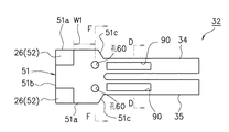
図1は、本発明の第1の実施形態にかかる圧電デバイスである例えば圧電振動子30の概略斜視図であり、図2は、この圧電振動子30のC−C線切断断面図である。また、図3は圧電振動片32の平面図、図4は図3のD−D線切断端面図、図5は図3のF−F線切断端面図である。
これらの図において、圧電振動子30は、パッケージ36内に圧電振動片32を収容している。
【0024】
パッケージ36は、例えば、絶縁材料として、酸化アルミニウム質のセラミックグリーンシートを成型して形成される複数の基板を積層した後に、焼結して形成されている。すなわち、図2に示されるように、この実施形態では、パッケージ36は、下から第1の積層基板36a、第2の積層基板36bを重ねて形成されている。そして、第2の積層基板36bの内側に所定の孔を形成することで、第2の積層基板36bを第1の積層基板36aに積層した場合に、圧電振動片32を収容する所定の内部空間S1を形成するようにされている。
また、パッケージ36の開放された上端にある開放端面36cに、例えば、低融点ガラス等のロウ材38を介して、蓋体39が接合されることにより、封止されている。
【0025】
パッケージ36の内部空間S1内の図2における左端部付近において、内部空間S1に露出して底部を構成するベースとなる第1の積層基板36aには、AuまたはNiメッキが施された電極部31,31が形成されている。この電極部31,31は、外部と接続されて、駆動電圧を供給するものであり、図1に示すように、内部空間S1内の長手方向の側面に接して、所定の間隔を隔てて形成されている。
【0026】
この所定の間隔を隔てた電極部31,31の上には、接着剤である例えば導電性接着剤43,43が塗布されている。導電性接着剤43,43としては、接合力を発揮する接着剤成分としての合成樹脂剤に、銀製の細粒等の導電性の粒子を含有させたエポキシ系またはポリイミド系、またはシリコーン系導電性接着剤等を利用することができる。
【0027】
そして、この導電性接着剤43,43の上に、基部51の振動腕34,35と反対側の端部(図2において左端部)51bであって、基部51の幅方向両端付近が対向するようにして、圧電振動片32が載置されている。
このようにして、圧電振動片32の基部51の一部は、導電性接着剤43,43を介してパッケージ36に支持固定され、また、パッケージ36に設けた電極部31,31が、圧電振動片32に駆動電圧を供給するようになっている。
【0028】
圧電振動片32は、例えば水晶で形成されており、水晶以外にもタンタル酸リチウム、ニオブ酸リチウム等の圧電材料を利用することができる。本実施形態の場合、圧電振動片32は、小型に形成して、必要な性能を得るために、特に図示する形状とされている。
すなわち、圧電振動片32は、導電性接着剤43,43によりパッケージ36と固定される基部51から、図3において右方に向けて、二股に別れて平行に延びる一対の振動腕34,35を備えており、全体が音叉のような形状とされた、所謂、音叉型圧電振動片が利用されている。
【0029】
振動腕34,35は、図1ないし図3に示すように、それぞれに圧電振動片32の長手方向に沿って延びる長溝90,90が設けられている。この長溝90,90は、図4に示すように、振動腕34,35の上面および下面に設けられており、長溝90,90を設けた振動腕34,35の断面形状を略H型としている。このような長溝90,90を設けることで、図4に示すように、振動腕34,35に厚みが薄い箇所が形成され、振動腕34,35内の電界が厚み方向Eに沿って、効率よく発生するため、圧電振動片32の電界効率を高めることができる。このため、長溝90,90を設けることで、圧電振動片32のクリスタルインピーダンス値(以下、「CI値」と云う。)を低く抑えることができる。したがって、このような圧電振動片32のCI値を、従来の圧電振動片と同様のCI値となるように形成して、振動腕34,35の長さを短くして、圧電振動片32を小型化できる。
【0030】
基部51は、図1および図2に示すように、表面と裏面(図2において、導電性接着剤43,43と主に接触している面)とが平行に形成されて、厚みが均一になっている。また、基部51は、図3に示すように、圧電振動片32の短手方向の端面51a,51aが対称となっており、この端面51a,51aと、圧電振動片32の長手方向であって振動腕34,35と反対側の端面51bとが交わる部分は垂直となっている。また、端面51a,51aと振動腕34,35とが交わる付近51cは、基部51の幅が振動腕34,35に向かうにつれて狭まっている。
このような基部51において、圧電振動片32に導電性接着剤43,43により固定された箇所52,52(図2において斜線で示された箇所)には、駆動電圧を伝えるための引出電極26,26が設けられている。
【0031】
ここで、基部51は、導電性接着剤43,43により固定された箇所52,52、すなわち引出電極26,26と振動腕34,35との間の領域に、図1ないし図3に示すように、複数の孔60,60が形成されている。
この孔60,60は、振動腕34,35の振動が、基部51の導電性接着剤43,43により固定された箇所52,52に伝達することを有効に防止するための孔である。
【0032】
具体的には、孔60,60は、図3に示すように、均一な厚みを有する基部51のうち、一対の振動腕34,35のそれぞれの根元付近に形成されている。この孔60,60は、丸孔であり、図5に示すように、基部51の厚み方向に貫通した貫通孔で形成されている。
すなわち、基部51に設けられた孔60,60の周辺は、基部51が構造的に弱い部分となる。このため、振動腕34,35から伝達された振動により生じる基部の応力は、孔60,60の周辺に集中し、基部51の導電性接着剤43,43により固定された箇所52,52については、応力が小さくなる。
【0033】
また、この孔60,60は、振動腕34,35の根元に形成されているため、孔60,60と、基部51の振動腕34,35とは反対側の端部51bの付近にある導電性接着剤43,43により固定された箇所52,52との距離W1は離れている。そうすると、応力が集中した箇所から遠くなるにつれて、応力は小さくなるので、基部51の導電性接着剤43,43により固定された箇所52,52の応力を小さくできる。
【0034】
しかも、振動腕34,35の振動は、それぞれの根元を通って基部51に伝達されるため、孔60,60が、振動腕34,35の根元付近に形成されていることで、振動をより孔60,60の周辺に集中させ易く、基部51の孔60,60以外の部位に振動が逃げてしまうことを有効に防止できる。
【0035】
図6は、従来の圧電振動子について、製造した複数の圧電振動子のCI値を測定した図であり、図7は、複数の圧電振動子30について、上述のように振動腕34,35のそれぞれの根元付近に、貫通した丸孔60,60を形成して、CI値を測定した図である。
図6で示されるように、従来における複数の圧電振動子のCI値を測定したところ、70kΩを中心にした各製品毎にばらついたCI値が測定され、標準偏差は18.0kΩであった。このようにCI値がばらつく要因は、圧電振動子の小型化に伴い、各製品を同一に形成することは困難であり、さらに、基部の導電性接着剤により固定された箇所の大きさにもばらつきが生ずるため、振動漏れの状態が製品毎に異なってしまうからである。
【0036】
ところが、図7で示されるように、本実施形態のように振動腕34,35のそれぞれの根元付近に、貫通した丸孔60,60を形成した複数の圧電振動子30のCI値を測定したところ、40kΩを中心にした比較的ばらつきの少ないCI値が測定され、標準偏差は1.6kΩであることが確認された。すなわち、たとえ各製品毎の形状が異なり、基部51の導電性接着剤43,43により固定された箇所52,52の大きさにばらつきが有ったとしても、振動腕34,35からの振動が、基部51の導電性接着剤43,43により固定された箇所52,52に漏れないため、CI値のばらつきを抑制できた。
【0037】
本発明の第1の実施形態は以上のように構成されている。このため、たとえ圧電振動子30を小型に形成し、振動腕34,35の形状が製品毎にばらついていても、振動腕34,35からの振動が、基部51の導電性接着剤43,43により固定された箇所52,52に漏れることを有効に防止して、製品毎にCI値のばらつきの少ない、優れた振動特性を備えた圧電デバイス30を実現できる。
なお、孔60,60は、振動腕34,35の根元に丸孔で形成されているが、基部51の導電性接着剤43,43により固定された箇所52,52と振動腕34,35との間の領域に、応力を集中できる孔であれば、これに限らず、例えば、図8に示すように多角形の貫通孔であってもよい。
【0038】
図9および図10は、本発明の第1の実施形態にかかる第1の変形例であって、図9は、圧電デバイスの特徴的部分である圧電振動片70の平面図であり、図10は、図9のG−G線切断端面図である。
これらの図において、図1ないし図8の圧電振動子30と同一の構成には、共通する符号を付して重複する説明は省略し、相違点を中心に説明する。
【0039】
この圧電振動片70において、第1の実施形態と異なるのは、基部51に設けた孔の形状等を変えた点のみである。
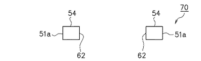
すなわち、基部51に設けた孔は、圧電振動片70の短手方向の両側壁51a,51a側に細枠54,54を残すようにして、短手方向に沿って設けた長孔62により形成されている。また、この長孔62は、図10に示されるように貫通孔となっている。
【0040】
本第1の実施形態にかかる第1の変形例は、以上のように構成され、このため、第1の実施形態と同様の作用効果を発揮する。さらに、第1の実施形態比べて、細枠54,54は、より基部51の構造的に弱い部分となるため、細枠54,54の周辺に、より応力が集中することになる。したがって、第1の発明に比べて、より振動が基部51の導電性接着剤43,43により固定された箇所52,52に漏れることを防止できる。
【0041】
図11および図12は、本発明の第2の実施形態であって、図11は、圧電デバイスの特徴的な部分である圧電振動片72の平面図であり、図12は、図11のH−H線切断端面図である。
これらの図において、図1ないし図10の圧電振動子30と同一の構成には、共通する符号を付して重複する説明は省略し、相違点を中心に説明する。
この圧電振動片72において、第1の実施形態と異なるのは、基部51に設けた孔の形状等を変えた点のみである。
【0042】
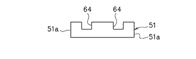
すなわち、図11で示すように、圧電振動片72の基部51であって、振動腕34,35の根元付近には、複数の孔64,64が形成されている。この孔64,64は、図12においては、貫通しておらず、有底となっている。なお、この有底の孔64,64は、図11および図12においては、表面側(導電性接着剤43,43が付着しない面)に設けられているが、裏面側に設けられていても勿論よい。
【0043】
本第2の実施形態は以上のように構成され、このため、第1の実施形態と同様の作用効果を発揮し、さらに、基部51の剛性を上げることができる。これにより、圧電デバイス30の落下によって圧電振動片72の基部51が振れてしまうことを有効に防止できる。したがって、基部51が不必要に振動してしまうことによる振動腕34,35の振動特性への影響を小さくできる。
【0044】
なお、第1の実施形態の第1の変形例で示した、基部51の両側壁51a、51a側に細枠54,54を残すようにして、短手方向に沿って設けた長孔62(図9参照)についても、基部51を長孔62の部分で幅方向に切断した図13に示すように、有底に形成してもよい。
【0045】
図14および図15は、本発明の第2の実施形態の第1の変形例であって、図14は、圧電デバイスの特徴的な部分である圧電振動片74の平面図であり、図15は、図14のJ−J線切断端面図である。
これらの図において、図11および図12の圧電振動片72と同一の構成には、共通する符号を付して重複する説明は省略し、相違点を中心に説明する。
この圧電振動片74において、第2の実施形態と異なるのは、基部51に設けた孔の形状等を変えた点のみである。
【0046】
すなわち、図14および図15で示すように、圧電振動片74の基部51であって、振動腕34,35の根元付近には、表面に複数の有底の孔66a,66aが、裏面(導電性接着剤43,43が主に付着している面)に複数の有底の孔66b,66bが、それぞれ対向するように形成されている。この各有底の孔66a,66a,66b,66bは、第2の実施形態における孔64と同様の深さ及び開口面積を有し、表面側の有底の孔66a,66aの底面と、裏面側の有底の孔66b,66bの底面との間53,53は、基部51に一定の強度が保持できるように、一定の間隔が形成されている。
【0047】
本発明の第2の実施形態の第1の変形例は以上のように構成されており、このため、表面側の有底の孔66a,66aの底面と、裏面側の有底の孔66b,66bの底面との間53,53に構造的に弱い部分をつくることができる。したがって、第1の実施形態と比べると、基部51の剛性を高めることができ、第2の実施形態と比べると、より振動が基部51の導電性接着剤43,43により固定された箇所52,52に漏れることを防止できる。
【0048】
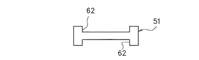
なお、第1の実施形態の第1の変形例で示した、基部51の両側壁51a、51a側に細枠54,54を残すようにして、短手方向に沿って設けた長孔62(図9参照)についても、基部51を長孔62の部分で幅方向に切断した図16に示すように、表面および裏面に有底の孔62を設けるように形成してもよい。
【0049】
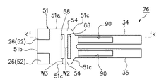
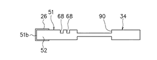
図17および図18は、本発明の第3の実施形態であって、図17は、圧電デバイスの特徴的な部分である圧電振動片76の平面図であり、図18は、図17のK−K線切断端面図である。
これらの図において、図1ないし図16の圧電振動子30と同一の構成には、共通する符号を付して重複する説明は省略し、相違点を中心に説明する。
この圧電振動片76において、他の実施形態と異なるのは、基部51に設けた孔の形状等を変えた点のみである。
【0050】
すなわち、図17で示すように、基部51には、圧電振動片76の短手方向の両側壁51a,51a側に細枠54,54を残すようにして、短手方向に沿って設けた複数の長孔68,68が形成されている。この複数の長孔68,68は、図17においては、長孔68と長孔68との間隔W2が、細枠54,54の幅W3と同等若しくはそれ以下になるように形成されている。また、長孔68,68は、図18に示されるように、貫通しておらず、有底に形成されている。
【0051】
本第3の実施形態は以上のように構成され、これにより、振動腕34,35の振動により生ずる基部の応力は、基部51の構造的に弱い部分である細枠54,54に集中すると共に、この細枠54,54と同等以下の構造的に弱い部分である長孔68,68間に集中する。したがって、例えば、図13に示す有底の長孔62が一箇所に設けられた圧電振動子に比べて、基部51の導電性接着剤43,43により固定された箇所52,52に振動が漏れることをより有効に防止できる。
なお、図19に示すように、有底の長孔68,68は、基部51の表面および裏面(導電性接着剤43,43が主に付着している面)に設けられていても勿論よい。
【0052】
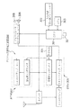
図20は、本発明の上述した実施形態に係る圧電デバイスを利用した電子機器の一例としてのデジタル式携帯電話装置300の概略構成を示す図である。
図において、送信者の音声を受信するマイクロフォン308及び受信内容を音声出力とするためのスピーカ309を備えており、さらに、送受信信号の変調及び復調部に接続された制御部としての集積回路等であるコントローラ301を備えている。
コントローラ301は、送受信信号の変調及び復調の他に画像表示部としてのLCDや情報入力のための操作キー等でなる情報の入出力部302や、RAM、ROM等でなる情報記憶手段303の制御を行なうようになっている。このため、コントローラ301には、例えば、圧電デバイス30が取り付けられて、この出力周波数をコントローラ301に内蔵された所定の分周回路(図示せず)等により、制御内容に適合したクロック信号として利用するようにされている。このコントローラ301に取り付けられる圧電デバイス30は、圧電デバイス30単体でなくても、圧電デバイス30と、所定の分周回路等を組み合わせた発振器であってもよい。
コントローラ301は、さらに、温度補償水晶発振器(TCXO)305と接続され、温度補償水晶発振器305は、送信部307と受信部306に接続されている。これにより、コントローラ301からの基本クロックが、環境温度が変化した場合に変動しても、温度補償水晶発振器305により修正されて、送信部307及び受信部306に与えられるようになっている。
【0053】
このように、デジタル式携帯電話装置300のような電子機器に、上述した実施形態に係る圧電振動子30を利用することにより、圧電振動片の振動漏れを防止して、優れた振動特性を備えた圧電デバイスを小型にしても得ることができ、デジタル式携帯電話装置300全体の小型化に寄与できる。
【0054】
本発明は上述の実施形態に限定されない。各実施形態の各構成はこれらを適宜相互に組み合わせたり、省略し、図示しない他の構成と組み合わせることができる。
この発明の圧電デバイスは、パッケージ内に圧電振動子と、これに接続される電子部品を含むものであれば、圧電発信器、圧電振動子、フィルタ等その名称を問わずに適用できるものである。
【図面の簡単な説明】
【図1】本発明の第1の実施形態にかかる圧電デバイスである例えば圧電振動子の概略斜視図。
【図2】図1のC−C線切断断面図。
【図3】本発明の第1の実施形態にかかる圧電振動片の平面図。
【図4】図3のD−D線切断端面図。
【図5】図3のF−F線切断端面図。
【図6】従来の圧電振動子について、製造した複数の圧電振動子のCI値を測定した図。
【図7】複数の圧電振動子について、各振動腕のそれぞれの根元付近に、貫通した丸孔を形成して、CI値を測定した図。
【図8】圧電振動片に設けた貫通孔を多角形にした図。
【図9】本発明の第1の実施形態にかかる第1の変形例であって、圧電デバイスの特徴的部分である圧電振動片の平面図。
【図10】図9のG−G線切断端面図。
【図11】本発明の第2の実施形態であって、圧電デバイスの特徴的な部分である圧電振動片の平面図。
【図12】図11のH−H線切断端面図。
【図13】基部の両側壁側に細枠を残すようにして、短手方向に沿って設けた長孔について、基部を長孔の部分で幅方向に切断した図。
【図14】本発明の第2の実施形態の第1の変形例であって、圧電デバイスの特徴的な部分である圧電振動片の平面図。
【図15】図14のJ−J線切断端面図。
【図16】基部の両側壁側に細枠を残すようにして、短手方向に沿って設けた長孔について、基部を長孔の部分で幅方向に切断した図。
【図17】本発明の第3の実施形態であって、圧電デバイスの特徴的な部分である圧電振動片の平面図。
【図18】図17のK−K線切断端面図。
【図19】図18の孔を表面および裏面に設けた図。
【図20】本発明の各実施形態に係る圧電デバイスを利用した電子機器の一例としてのデジタル式携帯電話装置の概略構成を示す図。
【図21】従来の圧電デバイスである例えば圧電振動子の平面図。
【図22】図21のA−A線切断断面図。
【図23】各振動腕に印加される電圧を示すグラフ。
【図24】図21のB−B線切断端面図。
【符号の説明】
30・・・圧電振動子、36・・・パッケージ、31・・・電極部、43・・・導電性接着剤、32,70,72,74,76・・・・・圧電振動片、34,35・・・振動腕、51・・・基部、60,62,64,66a,66b,68・・・孔、26・・・引出電極。[0001]
TECHNICAL FIELD OF THE INVENTION
The present invention relates to a piezoelectric device, a mobile phone device using the piezoelectric device, and an electronic apparatus.
[0002]
[Prior art]
21 is a plan view of a conventional piezoelectric device, for example, a
In these drawings, for example, a
[0003]
The
[0004]
The piezoelectric
At the
[0005]
In this way, the
[0006]
[Patent Document 1] JP-A-2001-329552
[0007]
[Problems to be solved by the invention]
Incidentally, the voltages applied to the vibrating
[0008]
However, the above-described piezoelectric vibrating
[0009]
Therefore, the vibrations of the vibrating
[0010]
Further, if the
In addition, with the miniaturization of the piezoelectric vibrating
[0011]
An object of the present invention is to solve the above-described problems. Even when the piezoelectric vibrating piece is formed in a small size, by preventing vibration leakage of the piezoelectric vibrating reed, it is possible to suppress variations in the CI value quality and the like of the product, and provide an excellent It is an object of the present invention to provide a piezoelectric device having vibration characteristics, a mobile phone device and an electronic device using the piezoelectric device.
[0012]
[Means for Solving the Problems]
According to a first aspect of the present invention, there is provided a piezoelectric vibrating reed having a pair of vibrating arms extending in parallel from a base, and each of the pair of vibrating arms having a long groove extending along a longitudinal direction, A package accommodating the piezoelectric vibrating reed therein by supporting and fixing a part of the base via an adhesive, wherein the base has a uniform thickness, and This is achieved by a piezoelectric device in which a hole is provided in a region between a portion fixed by an agent and the vibrating arm.
[0013]
According to the configuration of the first aspect, the piezoelectric device has a pair of vibrating arms extending in parallel from the base, and each of the pair of vibrating arms is formed with a long groove extending in the longitudinal direction. And a package for accommodating the piezoelectric vibrating reed therein by supporting and fixing a part of the base via an adhesive. Therefore, the pair of vibrating arms that are not fixed to the package vibrate when a predetermined voltage is applied, and the vibration is transmitted to the base.
However, the base has a uniform thickness, and a hole is provided in a region between the portion fixed by the adhesive and the vibrating arm. Then, the periphery of the hole becomes a structurally weak portion, and the stress of the base generated by the vibration transmitted from the resonating arm concentrates on the periphery of the hole, and the stress is reduced at the portion fixed by the adhesive of the base. . For this reason, it is possible to effectively prevent the vibration from leaking into a portion fixed by the adhesive at the base.
Therefore, even if the piezoelectric device is formed in a small size, by preventing the vibration leakage of the piezoelectric vibrating reed, the variation in the CI value quality of the product is suppressed, and a piezoelectric device having excellent vibration characteristics and a mobile phone using the piezoelectric device are provided. Equipment and electronic equipment can be provided.
[0014]
A second invention is characterized in that, in the configuration of the first invention, the hole is formed near a base of each of the plurality of vibrating arms.
According to the configuration of the second aspect, the hole is formed near the base of each of the plurality of vibrating arms. For this reason, since the vibration of the vibrating arm is transmitted to the base through the base of each of the plurality of vibrating arms, the stress generated by the vibration of the vibrating arm can be more easily concentrated around the hole, and the vibration other than the hole in the base can be easily achieved. It is possible to effectively prevent the vibration from escaping to the part.
[0015]
In a third aspect based on the configuration of the first aspect, the hole is provided along the short direction so as to leave a narrow frame on both side walls in the short direction of the piezoelectric vibrating piece. Characterized by the following.
For this reason, similarly to the first invention, the thin frame portion of the base becomes a structurally weak portion, and stress is more concentrated around the thin frame. Therefore, compared to the first aspect, it is possible to prevent the vibration from leaking to a portion fixed by the adhesive at the base.
[0016]
A fourth invention is characterized in that, in the constitution of the third invention, a plurality of the long holes are formed.
Then, the stress at the base caused by the vibration of the vibrating arm is more concentrated around the plurality of slots than in the third aspect. For this reason, since the stress in the entire base is constant, the stress in the portion fixed by the adhesive becomes relatively small. Therefore, compared to the third aspect, it is possible to more effectively prevent the vibration from leaking from the base to the portion fixed by the adhesive.
[0017]
A fifth invention is characterized in that, in the configuration according to any one of the first to fourth inventions, the hole penetrates in a thickness direction of the base.
For this reason, the periphery of the hole is a structurally weaker portion than in the first to fourth aspects of the invention, and the stress generated by the vibration of the vibrating arm is more concentrated around the hole. Therefore, it is possible to more effectively prevent the vibration from leaking to the portion fixed by the adhesive at the base.
[0018]
A sixth invention is characterized in that, in the configuration according to any one of the first to fourth inventions, the hole is a bottomed hole.
Therefore, the rigidity of the base can be increased as compared with the fifth aspect. Therefore, it is possible to effectively prevent the base of the piezoelectric vibrating piece from swinging due to, for example, a drop of the piezoelectric device, and to reduce the influence on the vibration characteristics of the vibrating arm.
[0019]
A seventh invention is characterized in that, in the configuration of the sixth invention, the bottomed hole is provided on a front surface and a back surface of the base.
For this reason, the stress generated by the vibration of the vibrating arm is concentrated around the bottomed holes provided on the front surface and the back surface of the base, and compared with the sixth invention, the stress is fixed to the portion of the base fixed by the adhesive. Vibration is hardly transmitted.
[0020]
According to a ninth aspect of the present invention, there is provided a piezoelectric vibrating reed having a pair of vibrating arms extending in parallel from a base, and each of the pair of vibrating arms being formed with a long groove extending in a longitudinal direction. A cellular phone device which obtains a control clock signal by a piezoelectric device comprising: a package for accommodating the piezoelectric vibrating reed by supporting and fixing a part of the base via an adhesive. Wherein the base portion of the piezoelectric device has a uniform thickness, and is achieved by a mobile phone device in which a hole is provided in a region between the portion fixed by the adhesive and the vibrating arm. .
[0021]
According to a tenth aspect of the present invention, there is provided a piezoelectric vibrating reed having a pair of vibrating arms extending in parallel from a base, and each of the pair of vibrating arms being formed with a long groove extending in a longitudinal direction. And a package in which a part of the base is supported and fixed via an adhesive, and a package for accommodating the piezoelectric vibrating reed is provided to obtain a control clock signal by a piezoelectric device. The base of the piezoelectric device is achieved by an electronic device having a uniform thickness and a hole provided in a region between the portion fixed by the adhesive and the vibrating arm.
[0022]
BEST MODE FOR CARRYING OUT THE INVENTION
Hereinafter, preferred embodiments of the present invention will be described in detail with reference to the accompanying drawings.
Note that the embodiments described below are preferred specific examples of the present invention, and therefore, various technically preferable limitations are given. However, the scope of the present invention particularly limits the present invention in the following description. It is not limited to these forms unless otherwise stated.
[0023]
FIG. 1 is a schematic perspective view of, for example, a
In these drawings, the
[0024]
The
Further, a
[0025]
In the inner space S1 of the
[0026]
An adhesive, for example, a
[0027]
An end (left end in FIG. 2) 51b of the base 51 on the side opposite to the vibrating
In this manner, a part of the
[0028]
The piezoelectric vibrating
That is, the piezoelectric vibrating
[0029]
As shown in FIGS. 1 to 3, the vibrating
[0030]
As shown in FIGS. 1 and 2, the
In such a
[0031]
Here, as shown in FIGS. 1 to 3, the
The
[0032]
Specifically, as shown in FIG. 3, the
That is, around the
[0033]
Further, since the
[0034]
In addition, since the vibrations of the vibrating
[0035]
FIG. 6 is a diagram showing the measured values of CI of a plurality of manufactured piezoelectric vibrators for a conventional piezoelectric vibrator. FIG. 7 shows the results of measuring the
As shown in FIG. 6, when the CI value of a plurality of conventional piezoelectric vibrators was measured, the CI value varied for each product centering on 70 kΩ was measured, and the standard deviation was 18.0 kΩ. The reason why the CI value varies as described above is that it is difficult to form each product identically with the downsizing of the piezoelectric vibrator, and furthermore, the size of the portion fixed by the conductive adhesive at the base is also limited. This is because the state of vibration leakage differs from product to product due to variation.
[0036]
However, as shown in FIG. 7, the CI values of the plurality of
[0037]
The first embodiment of the present invention is configured as described above. Therefore, even if the
The
[0038]
FIGS. 9 and 10 show a first modified example according to the first embodiment of the present invention. FIG. 9 is a plan view of a piezoelectric vibrating
In these drawings, the same components as those of the
[0039]
The piezoelectric vibrating
That is, the holes provided in the
[0040]
The first modified example according to the first embodiment is configured as described above, and therefore exhibits the same operation and effect as the first embodiment. Furthermore, compared to the first embodiment, the
[0041]
FIGS. 11 and 12 show a second embodiment of the present invention. FIG. 11 is a plan view of a piezoelectric vibrating
In these drawings, the same components as those of the
The piezoelectric vibrating
[0042]
That is, as shown in FIG. 11, a plurality of
[0043]
The second embodiment is configured as described above. Therefore, the same operation and effect as those of the first embodiment can be exhibited, and the rigidity of the base 51 can be increased. Accordingly, it is possible to effectively prevent the
[0044]
In addition, the long holes 62 (provided along the lateral direction so as to leave the
[0045]
FIGS. 14 and 15 show a first modification of the second embodiment of the present invention. FIG. 14 is a plan view of a piezoelectric vibrating
In these drawings, the same components as those of the piezoelectric vibrating
The piezoelectric vibrating
[0046]
That is, as shown in FIGS. 14 and 15, a plurality of bottomed
[0047]
The first modification of the second embodiment of the present invention is configured as described above. Therefore, the bottom surfaces of the bottomed
[0048]
In addition, the long holes 62 (provided along the lateral direction so as to leave the
[0049]
17 and 18 show a third embodiment of the present invention. FIG. 17 is a plan view of a piezoelectric vibrating
In these drawings, the same components as those of the
This piezoelectric vibrating
[0050]
That is, as shown in FIG. 17, the
[0051]
The third embodiment is configured as described above, whereby the stress at the base caused by the vibration of the vibrating
As shown in FIG. 19, the
[0052]
FIG. 20 is a diagram illustrating a schematic configuration of a digital mobile phone device 300 as an example of an electronic apparatus using the piezoelectric device according to the above-described embodiment of the present invention.
In the figure, a
The controller 301 controls an information input /
The controller 301 is further connected to a temperature-compensated crystal oscillator (TCXO) 305, and the temperature-compensated
[0053]
As described above, by using the
[0054]
The invention is not limited to the embodiments described above. Each configuration of each embodiment can be appropriately combined with each other or omitted, and can be combined with another configuration (not shown).
The piezoelectric device of the present invention can be applied to any device including a piezoelectric oscillator, a piezoelectric oscillator, a filter, and the like, regardless of their names, as long as the package includes a piezoelectric oscillator and electronic components connected thereto. .
[Brief description of the drawings]
FIG. 1 is a schematic perspective view of, for example, a piezoelectric vibrator which is a piezoelectric device according to a first embodiment of the present invention.
FIG. 2 is a sectional view taken along line CC of FIG. 1;
FIG. 3 is a plan view of the piezoelectric vibrating reed according to the first embodiment of the present invention.
FIG. 4 is a sectional view taken along line DD of FIG. 3;
FIG. 5 is a sectional view taken along line FF of FIG. 3;
FIG. 6 is a diagram showing CI values of a plurality of manufactured piezoelectric vibrators measured for a conventional piezoelectric vibrator.
FIG. 7 is a diagram in which, for a plurality of piezoelectric vibrators, a penetrating round hole is formed near the base of each vibrating arm, and a CI value is measured.
FIG. 8 is a diagram in which a through hole provided in a piezoelectric vibrating piece is polygonal.
FIG. 9 is a first modified example according to the first embodiment of the present invention, and is a plan view of a piezoelectric vibrating reed that is a characteristic part of the piezoelectric device.
FIG. 10 is a sectional view taken along the line GG of FIG. 9;
FIG. 11 is a plan view of a piezoelectric vibrating reed which is a characteristic part of the piezoelectric device according to the second embodiment of the present invention.
FIG. 12 is a sectional view taken along line HH of FIG. 11;
FIG. 13 is a diagram in which a base is cut in a width direction at a portion of a long hole provided along a short direction so as to leave a thin frame on both side walls of the base.
FIG. 14 is a plan view of a piezoelectric vibrating reed, which is a first modification of the second embodiment of the present invention and is a characteristic part of a piezoelectric device.
FIG. 15 is a sectional view taken along line JJ of FIG. 14;
FIG. 16 is a view in which a base is cut in a width direction at a portion of a long hole provided along a short direction so as to leave a narrow frame on both side walls of the base.
FIG. 17 is a plan view of a piezoelectric vibrating reed which is a characteristic part of a piezoelectric device according to a third embodiment of the present invention.
18 is a sectional view taken along the line KK of FIG.
FIG. 19 is a diagram in which the holes of FIG. 18 are provided on the front surface and the back surface.
FIG. 20 is a diagram showing a schematic configuration of a digital mobile phone device as an example of an electronic apparatus using the piezoelectric device according to each embodiment of the present invention.
FIG. 21 is a plan view of a conventional piezoelectric device, for example, a piezoelectric vibrator.
FIG. 22 is a sectional view taken along line AA of FIG. 21;
FIG. 23 is a graph showing a voltage applied to each vibrating arm.
FIG. 24 is a sectional view taken along the line BB of FIG. 21;
[Explanation of symbols]
Claims (9)
前記基部は、厚みが均一であって、前記接着剤により固定された箇所と前記振動腕との間の領域に孔が設けられている
ことを特徴とする圧電デバイス。A piezoelectric vibrating reed having a pair of vibrating arms extending in parallel from the base, each of which has a long groove extending in the longitudinal direction, and supporting a part of the base via an adhesive; A piezoelectric device comprising: a package for fixing the piezoelectric vibrating reed therein so as to be fixed,
The piezoelectric device according to claim 1, wherein the base has a uniform thickness, and a hole is provided in a region between the portion fixed by the adhesive and the vibrating arm.
前記圧電デバイスの前記基部は、
厚みが均一であって、前記接着剤により固定された箇所と前記振動腕との間の領域に孔が設けられている
ことを特徴とする携帯電話装置。A piezoelectric vibrating reed having a pair of vibrating arms extending in parallel from the base, each of which has a long groove extending in the longitudinal direction, and supporting a part of the base via an adhesive; A cellular phone device configured to obtain a control clock signal by a piezoelectric device including a package that fixes the piezoelectric vibrating reed therein so as to be fixed,
The base of the piezoelectric device,
A mobile phone device having a uniform thickness, wherein a hole is provided in a region between the portion fixed by the adhesive and the vibrating arm.
前記圧電デバイスの前記基部は、
厚みが均一であって、前記接着剤により固定された箇所と前記振動腕との間の領域に孔が設けられている
ことを特徴とする電子機器。A piezoelectric vibrating reed having a pair of vibrating arms extending in parallel from the base, each of which has a long groove extending in the longitudinal direction, and supporting a part of the base via an adhesive; An electronic device configured to obtain a control clock signal by a piezoelectric device including a package that accommodates the piezoelectric vibrating reed therein, so as to be fixed,
The base of the piezoelectric device,
An electronic device having a uniform thickness, wherein a hole is provided in a region between the portion fixed by the adhesive and the vibrating arm.
Priority Applications (1)
| Application Number | Priority Date | Filing Date | Title |
|---|---|---|---|
| JP2002365528A JP2004200914A (en) | 2002-12-17 | 2002-12-17 | Piezoelectric device, mobile phone device and electronic device using piezoelectric device |
Applications Claiming Priority (1)
| Application Number | Priority Date | Filing Date | Title |
|---|---|---|---|
| JP2002365528A JP2004200914A (en) | 2002-12-17 | 2002-12-17 | Piezoelectric device, mobile phone device and electronic device using piezoelectric device |
Related Child Applications (1)
| Application Number | Title | Priority Date | Filing Date |
|---|---|---|---|
| JP2005256027A Division JP2006005970A (en) | 2005-09-05 | 2005-09-05 | Piezoelectric device, and mobile phone device and electronic apparatus using the piezoelectric device |
Publications (1)
| Publication Number | Publication Date |
|---|---|
| JP2004200914A true JP2004200914A (en) | 2004-07-15 |
Family
ID=32763063
Family Applications (1)
| Application Number | Title | Priority Date | Filing Date |
|---|---|---|---|
| JP2002365528A Withdrawn JP2004200914A (en) | 2002-12-17 | 2002-12-17 | Piezoelectric device, mobile phone device and electronic device using piezoelectric device |
Country Status (1)
| Country | Link |
|---|---|
| JP (1) | JP2004200914A (en) |
Cited By (13)
| Publication number | Priority date | Publication date | Assignee | Title |
|---|---|---|---|---|
| JP2006074793A (en) * | 2004-09-03 | 2006-03-16 | Eta Sa Manufacture Horlogere Suisse | Small crystal resonator |
| WO2007017992A1 (en) * | 2005-08-10 | 2007-02-15 | Daishinku Corporation | Piezoelectric vibration device and method for manufacturing same |
| JP2007049434A (en) * | 2005-08-10 | 2007-02-22 | Daishinku Corp | Piezoelectric vibrating piece and piezoelectric vibrating device |
| JP2007081698A (en) * | 2005-09-13 | 2007-03-29 | Daishinku Corp | Tuning fork type piezoelectric vibrating piece and piezoelectric vibrating device |
| JP2008249489A (en) * | 2007-03-30 | 2008-10-16 | Tdk Corp | Angular velocity sensor element and angular velocity sensor device |
| JP2009207022A (en) * | 2008-02-29 | 2009-09-10 | Nippon Dempa Kogyo Co Ltd | Piezoelectric vibration piece, piezoelectric device, and frequency adjusting method of tuning-fork piezoelectric vibrator |
| US7675224B2 (en) | 2005-04-27 | 2010-03-09 | Seiko Epson Corporation | Piezoelectric vibrating reed and piezoelectric device |
| JP2010157933A (en) * | 2008-12-27 | 2010-07-15 | Epson Toyocom Corp | Bending vibrating piece and electronic component |
| JP2010183540A (en) * | 2009-02-09 | 2010-08-19 | Seiko Instruments Inc | Piezoelectric vibration piece, piezoelectric vibrator, oscillator, and electronic equipment and radio wave clock |
| JP2010259023A (en) * | 2009-04-28 | 2010-11-11 | Kyocera Kinseki Corp | Crystal oscillator |
| WO2012108335A1 (en) * | 2011-02-07 | 2012-08-16 | 株式会社大真空 | Tuning-fork type piezoelectric vibrating reed and tuning-fork type piezoelectric vibrator |
| CN113556099A (en) * | 2021-06-11 | 2021-10-26 | 成都泰美克晶体技术有限公司 | Piezoelectric quartz crystal oscillation piece, resonator and oscillator |
| US11290082B2 (en) | 2017-03-30 | 2022-03-29 | Daishtnku Corporation | Tuning fork-type piezoelectric vibration piece and tuning fork-type piezoelectric vibrator using the vibration piece |
-
2002
- 2002-12-17 JP JP2002365528A patent/JP2004200914A/en not_active Withdrawn
Cited By (21)
| Publication number | Priority date | Publication date | Assignee | Title |
|---|---|---|---|---|
| US7253554B2 (en) | 2004-09-03 | 2007-08-07 | Eta Sa Manufacture Horlogere Suisse | Quartz resonator of small dimensions |
| EP1633042B1 (en) * | 2004-09-03 | 2010-05-05 | ETA SA Manufacture Horlogère Suisse | Quartz resonator of very small dimensions |
| JP2006074793A (en) * | 2004-09-03 | 2006-03-16 | Eta Sa Manufacture Horlogere Suisse | Small crystal resonator |
| US7675224B2 (en) | 2005-04-27 | 2010-03-09 | Seiko Epson Corporation | Piezoelectric vibrating reed and piezoelectric device |
| US7902731B2 (en) | 2005-08-10 | 2011-03-08 | Daishinku Corporation | Piezoelectric resonator device and method for manufacturing the same |
| WO2007017992A1 (en) * | 2005-08-10 | 2007-02-15 | Daishinku Corporation | Piezoelectric vibration device and method for manufacturing same |
| JP2007049434A (en) * | 2005-08-10 | 2007-02-22 | Daishinku Corp | Piezoelectric vibrating piece and piezoelectric vibrating device |
| JPWO2007017992A1 (en) * | 2005-08-10 | 2009-02-19 | 株式会社大真空 | Piezoelectric vibration device and manufacturing method thereof |
| JP2007081698A (en) * | 2005-09-13 | 2007-03-29 | Daishinku Corp | Tuning fork type piezoelectric vibrating piece and piezoelectric vibrating device |
| JP2008249489A (en) * | 2007-03-30 | 2008-10-16 | Tdk Corp | Angular velocity sensor element and angular velocity sensor device |
| JP2009207022A (en) * | 2008-02-29 | 2009-09-10 | Nippon Dempa Kogyo Co Ltd | Piezoelectric vibration piece, piezoelectric device, and frequency adjusting method of tuning-fork piezoelectric vibrator |
| JP2010157933A (en) * | 2008-12-27 | 2010-07-15 | Epson Toyocom Corp | Bending vibrating piece and electronic component |
| JP2010183540A (en) * | 2009-02-09 | 2010-08-19 | Seiko Instruments Inc | Piezoelectric vibration piece, piezoelectric vibrator, oscillator, and electronic equipment and radio wave clock |
| JP2010259023A (en) * | 2009-04-28 | 2010-11-11 | Kyocera Kinseki Corp | Crystal oscillator |
| WO2012108335A1 (en) * | 2011-02-07 | 2012-08-16 | 株式会社大真空 | Tuning-fork type piezoelectric vibrating reed and tuning-fork type piezoelectric vibrator |
| CN103250349A (en) * | 2011-02-07 | 2013-08-14 | 株式会社大真空 | Tuning-fork type piezoelectric vibrating reed and tuning-ork type piezoelectric vibrator |
| JP5333668B2 (en) * | 2011-02-07 | 2013-11-06 | 株式会社大真空 | Tuning fork type piezoelectric resonator element and tuning fork type piezoelectric vibrator |
| US8928208B2 (en) | 2011-02-07 | 2015-01-06 | Daishinku Corporation | Tuning fork-type piezoelectric resonator plate and tuning fork-type piezoelectric resonator |
| CN103250349B (en) * | 2011-02-07 | 2015-09-02 | 株式会社大真空 | Tuning-fork type piezoelectric vibrating pieces and tuning-fork type piezoelectric unit |
| US11290082B2 (en) | 2017-03-30 | 2022-03-29 | Daishtnku Corporation | Tuning fork-type piezoelectric vibration piece and tuning fork-type piezoelectric vibrator using the vibration piece |
| CN113556099A (en) * | 2021-06-11 | 2021-10-26 | 成都泰美克晶体技术有限公司 | Piezoelectric quartz crystal oscillation piece, resonator and oscillator |
Similar Documents
| Publication | Publication Date | Title |
|---|---|---|
| JP4281348B2 (en) | Piezoelectric vibrating piece, piezoelectric device using the piezoelectric vibrating piece, mobile phone device using the piezoelectric device, and electronic equipment using the piezoelectric device | |
| CN100468967C (en) | Piezoelectric device and mobile phone device and electronic equipment using piezoelectric device | |
| US8987977B2 (en) | Piezoelectric vibration reed, piezoelectric vibrator, oscillator, electronic instrument, and radio timepiece | |
| US6897737B2 (en) | Vibrating reed, vibrator, oscillator, and electronic device | |
| US6590315B2 (en) | Surface mount quartz crystal resonators and methods for making same | |
| JP3812724B2 (en) | Vibrating piece, vibrator, oscillator and electronic device | |
| TWI555328B (en) | Piezoelectric vibrator, piezoelectric vibrator, oscillator, electronic machine and radio clock | |
| KR20120098491A (en) | Piezoelectric vibration element, piezoelectric device provided with same and electric apparatus | |
| JP6080486B2 (en) | Piezoelectric vibrating piece, piezoelectric vibrator, oscillator, electronic device and radio clock | |
| JP2004208237A (en) | Piezoelectric device and mobile phone device using piezoelectric device and electronic device using piezoelectric device | |
| JP5819151B2 (en) | Piezoelectric vibrator, piezoelectric vibrator, oscillator, electronic device and radio clock | |
| JP2003258589A (en) | Piezoelectric device, radio clock using piezoelectric device, mobile phone device using piezoelectric device, and electronic device using piezoelectric device | |
| JP2006005970A (en) | Piezoelectric device, and mobile phone device and electronic apparatus using the piezoelectric device | |
| JP6200636B2 (en) | Piezoelectric vibrating piece, piezoelectric vibrator, oscillator, electronic device, and radio timepiece | |
| JP3975927B2 (en) | Piezoelectric vibrating piece, piezoelectric device using the piezoelectric vibrating piece, mobile phone device using the piezoelectric device, and electronic equipment using the piezoelectric device | |
| JP2005123828A (en) | Tuning fork type piezoelectric vibrating piece and piezoelectric device | |
| JP4020010B2 (en) | Piezoelectric vibrating piece, piezoelectric device using the piezoelectric vibrating piece, mobile phone device using the piezoelectric device, and electronic equipment using the piezoelectric device | |
| JP4020031B2 (en) | Piezoelectric vibrating piece, piezoelectric device using the piezoelectric vibrating piece, mobile phone device using the piezoelectric device, and electronic equipment using the piezoelectric device | |
| JP5912051B2 (en) | Piezoelectric vibrator, piezoelectric vibrator, oscillator, electronic device and radio clock | |
| JP2004120802A (en) | Vibrating reed, vibrator, oscillator and electronic equipment | |
| JP2004336207A (en) | Piezoelectric vibrating reed, piezoelectric device using the piezoelectric vibrating reed, mobile phone device using the piezoelectric device, and electronic equipment using the piezoelectric device | |
| JP2004297769A (en) | Crystal vibrating piece, method of manufacturing crystal vibrating piece, crystal device containing this crystal vibrating piece in package, and electronic device using crystal device | |
| JP2004134852A (en) | Piezoelectric device, method of manufacturing the same, mobile phone device using piezoelectric device, and electronic device using piezoelectric device | |
| JP2004282498A (en) | Piezoelectric vibrating reed, piezoelectric device using the same, and electronic device using the piezoelectric device | |
| JP2006339701A (en) | Piezoelectric vibrator |
Legal Events
| Date | Code | Title | Description |
|---|---|---|---|
| A621 | Written request for application examination |
Free format text: JAPANESE INTERMEDIATE CODE: A621 Effective date: 20050905 |
|
| RD04 | Notification of resignation of power of attorney |
Effective date: 20070403 Free format text: JAPANESE INTERMEDIATE CODE: A7424 |
|
| A977 | Report on retrieval |
Effective date: 20080118 Free format text: JAPANESE INTERMEDIATE CODE: A971007 |
|
| A131 | Notification of reasons for refusal |
Effective date: 20080129 Free format text: JAPANESE INTERMEDIATE CODE: A131 |
|
| A761 | Written withdrawal of application |
Free format text: JAPANESE INTERMEDIATE CODE: A761 Effective date: 20080327 |