JP2004201326A - ハイブリッド・データ修復システム - Google Patents
ハイブリッド・データ修復システム Download PDFInfo
- Publication number
- JP2004201326A JP2004201326A JP2003420251A JP2003420251A JP2004201326A JP 2004201326 A JP2004201326 A JP 2004201326A JP 2003420251 A JP2003420251 A JP 2003420251A JP 2003420251 A JP2003420251 A JP 2003420251A JP 2004201326 A JP2004201326 A JP 2004201326A
- Authority
- JP
- Japan
- Prior art keywords
- slice
- center
- edge
- data signal
- received data
- Prior art date
- Legal status (The legal status is an assumption and is not a legal conclusion. Google has not performed a legal analysis and makes no representation as to the accuracy of the status listed.)
- Granted
Links
- 230000008439 repair process Effects 0.000 title abstract description 34
- 238000000034 method Methods 0.000 claims abstract description 32
- 238000013507 mapping Methods 0.000 claims description 23
- 230000008569 process Effects 0.000 claims description 5
- 230000000630 rising effect Effects 0.000 abstract description 10
- 238000010586 diagram Methods 0.000 description 17
- 238000011084 recovery Methods 0.000 description 16
- 238000005070 sampling Methods 0.000 description 16
- 230000007704 transition Effects 0.000 description 16
- 230000003287 optical effect Effects 0.000 description 7
- 238000004891 communication Methods 0.000 description 4
- 239000006185 dispersion Substances 0.000 description 4
- 230000001360 synchronised effect Effects 0.000 description 4
- 230000008901 benefit Effects 0.000 description 3
- 238000004364 calculation method Methods 0.000 description 3
- 230000002688 persistence Effects 0.000 description 3
- 230000010363 phase shift Effects 0.000 description 3
- 238000004458 analytical method Methods 0.000 description 2
- 238000001514 detection method Methods 0.000 description 2
- 230000006872 improvement Effects 0.000 description 2
- 238000012544 monitoring process Methods 0.000 description 2
- 238000012545 processing Methods 0.000 description 2
- 230000004044 response Effects 0.000 description 2
- 238000012360 testing method Methods 0.000 description 2
- 239000005711 Benzoic acid Substances 0.000 description 1
- 230000005540 biological transmission Effects 0.000 description 1
- 238000004422 calculation algorithm Methods 0.000 description 1
- 238000012512 characterization method Methods 0.000 description 1
- 230000007812 deficiency Effects 0.000 description 1
- 238000009795 derivation Methods 0.000 description 1
- 230000000694 effects Effects 0.000 description 1
- 239000000835 fiber Substances 0.000 description 1
- 238000002372 labelling Methods 0.000 description 1
- 230000014759 maintenance of location Effects 0.000 description 1
- 238000012986 modification Methods 0.000 description 1
- 230000004048 modification Effects 0.000 description 1
- 230000010287 polarization Effects 0.000 description 1
- 238000001228 spectrum Methods 0.000 description 1
- 230000003068 static effect Effects 0.000 description 1
Images


Classifications
-
- H—ELECTRICITY
- H04—ELECTRIC COMMUNICATION TECHNIQUE
- H04L—TRANSMISSION OF DIGITAL INFORMATION, e.g. TELEGRAPHIC COMMUNICATION
- H04L7/00—Arrangements for synchronising receiver with transmitter
- H04L7/02—Speed or phase control by the received code signals, the signals containing no special synchronisation information
- H04L7/033—Speed or phase control by the received code signals, the signals containing no special synchronisation information using the transitions of the received signal to control the phase of the synchronising-signal-generating means, e.g. using a phase-locked loop
-
- H—ELECTRICITY
- H04—ELECTRIC COMMUNICATION TECHNIQUE
- H04L—TRANSMISSION OF DIGITAL INFORMATION, e.g. TELEGRAPHIC COMMUNICATION
- H04L25/00—Baseband systems
- H04L25/02—Details ; arrangements for supplying electrical power along data transmission lines
- H04L25/06—DC level restoring means; Bias distortion correction ; Decision circuits providing symbol by symbol detection
- H04L25/061—DC level restoring means; Bias distortion correction ; Decision circuits providing symbol by symbol detection providing hard decisions only; arrangements for tracking or suppressing unwanted low frequency components, e.g. removal of DC offset
Landscapes
- Engineering & Computer Science (AREA)
- Computer Networks & Wireless Communication (AREA)
- Signal Processing (AREA)
- Power Engineering (AREA)
- Dc Digital Transmission (AREA)
- Detection And Prevention Of Errors In Transmission (AREA)
Abstract
【解決手段】データ修復回路では、各データ・ビットに対する着信データの複数のスライス回路の出力、たとえば、アイの中心で、またはその近くで取られた1つまたは複数のスライス回路の出力と、アイの立ち上がりおよび/または立下りで、またはそれらの近くで取られた1つまたは複数のスライス回路の出力が、従来技術と比較してビット誤り率を抑える方法で処理される。クロックおよびデータ修復(CDR)回路を改善するために、データ修復回路を最新技術のクロック修復回路と組み合わせることができる。
【選択図】図1
Description
Alexander,J.D.H.、「Clock Recovery From Random Binay Signals」、Electronic Letters、第11巻、541〜542頁、1975
図1は、本発明の一実施形態による高速データ受信器のデータ修復回路(DRC)を示すブロック図である。図から分かるように、DRC 102は、シリアル・データ入力(SDI)104と受信クロック(RCLK)106の両方から供給され、シリアル・データ・アウト(SDO)108を出力する。特定の実施態様に基づいて、DRC 102を出入りする信号は、差動または非差動であってよく、いかなる所与の論理系統(たとえば、CMOS、TTL、ECL)にでも対応することができるということに留意されたい。同期システムでは典型的なことであるが、RCLK 106は、SDI 104と共に送信器によって供給することができる。別法として、非同期実施態様では、RCLK 106は、クロック修復回路によってSDI04から局所的に導出することができる。上述のように、図1に示すデータ修復機能を実施するには複数の手法がある。本発明のある実施形態によれば、次節で説明するように、着信データの別個のスライス回路の組合せが使用される。
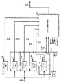
図2のデータ修復のブロック図は、本発明の一実施形態を示している。図から分かるように、この実施形態は、5つの別個のスライス回路(すなわち、電圧比較器)を使用する。具体的には、SDI 104は202から210までの5つのスライス回路すべてに平行に供給する。RCLK 106は、第1の3つのスライス回路202〜206と、スライス回路論理212と、フェーズ・シフト回路214とを供給する。フェーズ・シフト回路214は、RCLKP 216を生成するためにRCLK 106を180度(すなわち、RCLK 106の1/2の期間だけ)フェーズ・シフトし、このRCLKP 216は最後の2つのスライス回路208および210とスライス回路論理212とに供給する。スライス回路論理212は、5つのスライス回路の出力、すなわちSOA 218、SOB 220、SOC 222、SOD 224、およびSOE 226を追加的に受信し、出力SDO 108を生成するためにそれらを使用する。これらの要素のそれぞれに関して次節でより詳細に検討する。
202から210のスライス回路のそれぞれは、シリアル・データ入力信号SDI 104とスライス回路固有の電圧しきい値の間の電圧比較を実行する。スライス回路が信号SDIをサンプリングする時点で、信号SDIに関連する電圧がスライス回路固有のしきい値電圧よりも大きい場合、スライス回路は論理「1」を出力する。そうでない場合、スライス回路は論理「0」を出力する。
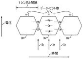
雑音がない場合、電圧しきい値Cmを使用して時間Smで取られるようなミッドデータまたは一時的な「アイの中心」しきい値比較は、SDI 104(図3の3つのアイダイヤグラムの中心のアイ302によって表される)のビットnのデータ情報を修復するために十分であるべきである。

ある種の通信システムは、アイのエッジよりもアイの中心で、信号の雑音破損からより多く影響を受ける。したがって、たとえば、受信器で観察されるアイダイヤグラムが「閉じている」ように見えるほど雑音が多いシステムは、アイのエッジはまだ比較的クリーンな場合がある。このようなシステムでは、アイの中心だけでサンプリングすることによってデータを修復することは困難な場合がある。しかし、アイのエッジで特定の方法でサンプリングすることによって、データ修復性能を改善することができる。
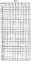
他の行は、表2に関して既に検討した解釈を考慮する同様の方法で完了される。
(アイの中心のスライス回路とアイのエッジのスライス回路の組合せ)
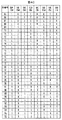
図2および3、ならびに図5の表4によって表される本発明の一実施形態では、表4のSDO(n)に対する値を導出するために一組の工程が行われる。まず、次式(1)に従って表1の8つの順列のそれぞれに対して重み付けされたアイの中心の推定値nw(Sm)iが計算される。
nw(Sm)i=(2*n1i−1)*CW1i (1)
上式で、CW1iは表1の列7、行iの数値の「信頼値」であり(ここで、高=1、中=0.5、低=0である)、n1iは表1の列4、行iのnの値である。次に、次式(2)に従って表3の16の順列のそれぞれに対して重み付けされた遷移の推定値nw(Sab)jが計算される。
nw(Sab)j=(2*n3j−1)*CW3j (2)
上式で、CW3jは表3の列10、行jの「信頼値」であり(ここで、一貫した結果は数値による信頼値1にマッピングされ、不整合な結果は数値による信頼値0にマッピングされる)、n3jは表3の列7、行jの値である。最後に、表4のSDO(n)に対する値nkが図6のプロシージャに従って計算される。
nw(Sm)1=(2*n11−1)*CW11=(2*0−1)*1=−1
である。式(2)に従うと、
nw(Sab)4=(2*n34−1)*CW34=(2*0−1)*0=0
である。図6の行4に従うと、
n4=nw(Sm)1+nw(Sab)4=−1+0=−1
である。図6の行5を適用すると、−1は0よりも大きくないのでn4=0である。
ここまで説明した実施形態は、対象のデータ・ビット(すなわち、ビットn)に関してアイの中心から得られるスライス回路の結果とアイの前後のエッジから得られるスライス回路の結果とを組み合わせることに焦点を合わせた。一般に、データ・ビットを推定するために使用される論理の対象データ・ビットの前および/または後の異なる時間のうちいくつかで取られたスライス回路情報の異なる組合せをいくつでも含むことができる。この情報は、限定はしないが、(1)ビットn−1に対して計算された値、(2)サンプル時間Sbで取られたアイのエッジのスライス回路出力SOD(Sb)とSOE(Sb)、(3)サンプル時間Smで取られたアイの中心のスライス回路出力SOA(Sm)、SOB(Sm)、およびSOC(Sm)、(4)サンプル時間Saで取られたアイのエッジのスライス回路出力SOD(Sa)およびSOE(Sa)、および(5)ビットn+1に対して計算された値を含む。別の実施態様では、ビットnに対する値を決定するためにこの情報の別の対象を組み合わせることができる。さらに、本発明の別の実施形態は、1つまたは複数のマルチビットのスライス回路(すなわち、高位ADC)を含めて異なる数のアイの中心のスライス回路とアイのエッジのスライス回路を有することができる。ある実施態様では、アイの中心の情報だけが計算されたデータ・ビットnの指定の信頼水準よりも少ない結果を生じる場合にだけアイのエッジの情報が使用される。別法として、他の実施態様では、アイのエッジの情報だけが計算されたデータ・ビットnの指定の信頼水準よりも少ない結果を生じる場合にだけアイの中心の情報が使用される。
図7の3つのアイダイヤグラムは、本発明の別の例示の実施形態を示している。このダイヤグラムでは、さまざまなスライス回路に対するしきい値、実現可能な結果、およびスライシング時間が示されている。これらのしきい値は、周期ごとに再利用される5つの固有のスライス回路のしきい値に対応する。ブロック702は、周期n中に適用されるような5つのスライス回路のしきい値を図示している。最初の2つのスライス回路は、時間T1(n)でn番目の周期の先頭のエッジでのしきい値704および706を使用し、一方、他の3つのスライス回路は、時間T2(n)でn番目の周期のアイの中心でのしきい値708、710、および712を使用する。これらのスライス回路の出力は、矛盾する結果を排除し、T1(n)およびT2(n)に対応する2タプルの値{V1(n)、V2a(n)}を得るように処理される。ここで、V1(n)は、「Hi」、「Mid」、または「Lo」の値を有し、V2a(n)は、「Hi」、「Mid−Hi」、「Mid−Lo」、または「Lo」の値を有する。V2a(n)はV2b(n)を得るよう処理される。ここで、V2b(n)は、次の関係に従って「Hi」または「Lo」の値に割り当てられる。
V2a(n)が「Hi」または「Mid−Hi」であれば、V2b(n)=「Hi」であり、
V2a(n)が「Mid−Lo」または「Lo」であれば、V2b(n)=「Lo」である。
本発明の一実施形態は、図8に示すようなクロックおよびデータ修復回路(CDR)を改善するために、最新技術のクロック修復回路を図2のデータ修復回路と組み合わせる。
Claims (10)
- 受信したデータ信号からデータを修復するための装置において、
(a)(1)エッジ・サンプルを生成するために、受信したデータ信号を、1つまたは複数のスライス回路しきい値の第1の組を使用して実質的にシンボル間隔のエッジでスライスし、
(2)中心サンプルを生成するために、受信したデータ信号を、1つまたは複数のスライス回路しきい値の第2の組を使用して実質的にシンボル間隔の中心でスライスする
ように構成された1組のスライス回路と、
(b)エッジ・サンプルと中心サンプルに基づいて、受信したデータ信号のデータ・ビットに対する値を決定するように構成された論理ブロックとを含む装置。 - エッジ・サンプルは、実質的に各シンボル間隔の前のエッジで取られた2つのスライス回路の出力と、実質的に各シンボル間隔の後のエッジで取られた2つのスライス回路の出力とを含み、
中心サンプルは、実質的に各シンボル間隔の中心で取られた3つのスライス回路の出力を含む請求項1に記載の発明。 - シンボル間隔nに対して、中心サンプルが、実質的にシンボル間隔n−1の中心で取られたスライス回路の出力と、実質的にシンボル間隔n+1の中心で取られたスライス回路の出力とをさらに含む請求項2に記載の発明。
- データ・ビットに対する値が、エッジのサンプル値と中心のサンプル値の異なる組合せを対応するデータ・ビット値にマッピングする論理ブロックへの入力としてエッジ・サンプルと中心サンプルを使用して決定される請求項1に記載の発明。
- 異なるマッピングが、データを修復する際に使用するために動的に選択される請求項4に記載の発明。
- 受信したデータ信号の各スライシングが指定したしきい値レベルに基づく請求項1に記載の発明。
- スライス回路のしきい値の第1と第2の組が同一でない請求項1に記載の発明。
- 受信したデータ信号を処理するために使用される局所的に生成されたクロックのフェーズと周波数との少なくとも一方がエッジ・サンプルと中心サンプルに基づいて調整される請求項1に記載の発明。
- 受信したデータ信号を処理するために使用される局所的に生成されたクロックを同期する方法において、
エッジ・サンプルを生成するために、受信したデータ信号を、1つまたは複数のスライス回路しきい値の第1の組を使用して実質的にシンボル間隔のエッジでスライスする工程と、
中心サンプルを生成するために、受信したデータ信号を、1つまたは複数のスライス回路しきい値の第2の組を使用して実質的にシンボル間隔の中心でスライスする工程と、
エッジ・サンプルと中心サンプルとに基づいて、局所的に生成されたクロックのフェーズと周波数との少なくとも一方を調整する工程と
を含み、
スライス回路しきい値の第1と第2の組は同一でなく、
現在のシンボル間隔に対して局所的に生成されたクロックを調整するために、
エッジ・サンプルが、実質的に現在のシンボル間隔の前のエッジで取られた単一スライス回路の出力を含み、
中心サンプルが、現在のシンボル間隔と前のシンボル間隔とに対するスライス回路の出力を含む方法。 - 受信したデータ信号からデータを修復する方法において、
エッジ・サンプルを生成するために、受信したデータ信号を、1つまたは複数のスライス回路しきい値の第1の組を使用して実質的にシンボル間隔のエッジでスライスする工程と、
中心サンプルを生成するために、受信したデータ信号を、1つまたは複数のスライス回路しきい値の第2の組を使用して実質的にシンボル間隔の中心でスライスする工程と、
エッジ・サンプルと中心サンプルとに基づいて、受信したデータ信号のデータ・ビットに対する値を決定する工程とを含む方法。
Applications Claiming Priority (1)
| Application Number | Priority Date | Filing Date | Title |
|---|---|---|---|
| US10/323,103 US7356095B2 (en) | 2002-12-18 | 2002-12-18 | Hybrid data recovery system |
Publications (2)
| Publication Number | Publication Date |
|---|---|
| JP2004201326A true JP2004201326A (ja) | 2004-07-15 |
| JP4309754B2 JP4309754B2 (ja) | 2009-08-05 |
Family
ID=30443978
Family Applications (1)
| Application Number | Title | Priority Date | Filing Date |
|---|---|---|---|
| JP2003420251A Expired - Fee Related JP4309754B2 (ja) | 2002-12-18 | 2003-12-18 | ハイブリッド・データ修復システム |
Country Status (3)
| Country | Link |
|---|---|
| US (1) | US7356095B2 (ja) |
| JP (1) | JP4309754B2 (ja) |
| GB (1) | GB2396536B (ja) |
Cited By (5)
| Publication number | Priority date | Publication date | Assignee | Title |
|---|---|---|---|---|
| WO2006129349A1 (ja) * | 2005-05-31 | 2006-12-07 | Fujitsu Limited | データ受信装置 |
| JP2013225821A (ja) * | 2012-04-23 | 2013-10-31 | Fujitsu Ltd | 補間回路および受信回路 |
| JP2013258681A (ja) * | 2012-05-14 | 2013-12-26 | Ricoh Co Ltd | データ受信装置及びデータ通信システム |
| JP2016001872A (ja) * | 2014-05-22 | 2016-01-07 | パナソニックIpマネジメント株式会社 | 受信装置 |
| JP2018125791A (ja) * | 2017-02-03 | 2018-08-09 | 富士通株式会社 | Cdr回路及び受信回路 |
Families Citing this family (20)
| Publication number | Priority date | Publication date | Assignee | Title |
|---|---|---|---|---|
| GB2397982B (en) * | 2003-01-28 | 2005-11-23 | Phyworks Ltd | Receiver |
| GB2401291B (en) * | 2003-05-01 | 2005-12-28 | Phyworks Ltd | Receiver |
| US7263122B2 (en) * | 2003-07-29 | 2007-08-28 | Synopsys, Inc. | Receiver based decision feedback equalization circuitry and techniques |
| US7366942B2 (en) * | 2004-08-12 | 2008-04-29 | Micron Technology, Inc. | Method and apparatus for high-speed input sampling |
| US7573967B2 (en) * | 2005-07-01 | 2009-08-11 | Slt Logic Llc | Input threshold adjustment in a synchronous data sampling circuit |
| US7813460B2 (en) * | 2005-09-30 | 2010-10-12 | Slt Logic, Llc | High-speed data sampler with input threshold adjustment |
| US7477850B2 (en) * | 2005-10-31 | 2009-01-13 | Agere Systems Inc. | Optical signal jitter reduction via electrical equalization in optical transmission systems |
| GB2446513B (en) * | 2007-02-09 | 2011-09-28 | Texas Instruments Ltd | Clock and data recovery which selects between over-sampling and baud-rate recovery |
| GB0806157D0 (en) * | 2008-04-04 | 2008-05-14 | Nxp Bv | Improved clock recovery of serial data signal |
| US8249199B2 (en) * | 2008-12-23 | 2012-08-21 | Oracle America, Inc. | Low jitter and high bandwidth clock data recovery |
| US9025702B2 (en) * | 2011-08-26 | 2015-05-05 | Fujitsu Limited | Method and apparatus for implementing slice-level adjustment |
| US8566761B2 (en) | 2011-11-21 | 2013-10-22 | International Business Machines Corporation | Network flow based datapath bit slicing |
| GB2504110A (en) * | 2012-07-18 | 2014-01-22 | Texas Instruments Inc | Data slicing level and timing adjustment |
| KR101786543B1 (ko) * | 2013-12-13 | 2017-10-18 | 인텔 코포레이션 | 오프셋 에지 샘플러들을 갖는 데이터 수신기 회로 |
| US9148235B1 (en) * | 2014-09-15 | 2015-09-29 | Global Unichip Corporation | Eye diagram measuring circuit and measuring method thereof |
| US9755866B2 (en) * | 2015-01-26 | 2017-09-05 | 9011579 Canada Incorporee | Direct digital sequence detector and equalizer based on analog-to-sequence conversion |
| US10069654B2 (en) * | 2015-11-10 | 2018-09-04 | Huawei Technologies Co., Ltd. | Methods to minimize the recovered clock jitter |
| US9917713B2 (en) | 2016-04-27 | 2018-03-13 | Hewlett Packard Enterprise Development Lp | Offset tunable edge slicer for sampling phase amplitude modulation signals |
| US10250418B2 (en) * | 2016-08-02 | 2019-04-02 | Keyssa Systems, Inc. | EHF receiver architecture with dynamically adjustable discrimination threshold |
| US11546127B2 (en) | 2021-03-18 | 2023-01-03 | Samsung Display Co., Ltd. | Systems and methods for symbol-spaced pattern-adaptable dual loop clock recovery for high speed serial links |
Family Cites Families (12)
| Publication number | Priority date | Publication date | Assignee | Title |
|---|---|---|---|---|
| US3479598A (en) | 1967-01-20 | 1969-11-18 | Bell Telephone Labor Inc | System for phase locking two pulse trains |
| US4339823A (en) * | 1980-08-15 | 1982-07-13 | Motorola, Inc. | Phase corrected clock signal recovery circuit |
| US4509180A (en) | 1982-03-15 | 1985-04-02 | Lgz Landis & Gyr Zug Ag | Method and an apparatus for correcting distortion of binary received signals |
| GB9102936D0 (en) * | 1991-02-12 | 1991-03-27 | Shaye Communications Ltd | Digital communications systems |
| US6570916B1 (en) * | 1997-03-04 | 2003-05-27 | Semiconductor Components Industries Llc | Adaptive equalization circuit and method |
| US6055436A (en) * | 1998-01-20 | 2000-04-25 | Motorola | Method and apparatus for detecting simulcast channel conditions |
| KR19990084784A (ko) | 1998-05-11 | 1999-12-06 | 윤종용 | 피.지.에이, 협대역 잡음제거 장치 및 이들을 구비한 초고속 디지털 가입자 회선 수신기 |
| CA2249800C (en) | 1998-10-06 | 2003-12-09 | Northern Telecom Limited | Eye quality monitor for a 2r regenerator |
| US6980586B1 (en) * | 1999-05-24 | 2005-12-27 | Intel Corporation | Pseudo-noise encoded digital data clock recovery |
| US6472918B1 (en) | 1999-08-23 | 2002-10-29 | Level One Communications, Inc. | Self-referencing slicer method and apparatus for high-accuracy clock duty cycle generation |
| US6349121B1 (en) | 2000-03-15 | 2002-02-19 | Memorylink, Inc. | Baseband data slicing method and apparatus |
| US7061995B2 (en) * | 2001-10-31 | 2006-06-13 | Intel Corporation | Apparatus and method to generate an adaptive slicer threshold for binary data |
-
2002
- 2002-12-18 US US10/323,103 patent/US7356095B2/en not_active Expired - Lifetime
-
2003
- 2003-12-10 GB GB0328624A patent/GB2396536B/en not_active Expired - Fee Related
- 2003-12-18 JP JP2003420251A patent/JP4309754B2/ja not_active Expired - Fee Related
Cited By (5)
| Publication number | Priority date | Publication date | Assignee | Title |
|---|---|---|---|---|
| WO2006129349A1 (ja) * | 2005-05-31 | 2006-12-07 | Fujitsu Limited | データ受信装置 |
| JP2013225821A (ja) * | 2012-04-23 | 2013-10-31 | Fujitsu Ltd | 補間回路および受信回路 |
| JP2013258681A (ja) * | 2012-05-14 | 2013-12-26 | Ricoh Co Ltd | データ受信装置及びデータ通信システム |
| JP2016001872A (ja) * | 2014-05-22 | 2016-01-07 | パナソニックIpマネジメント株式会社 | 受信装置 |
| JP2018125791A (ja) * | 2017-02-03 | 2018-08-09 | 富士通株式会社 | Cdr回路及び受信回路 |
Also Published As
| Publication number | Publication date |
|---|---|
| GB2396536B (en) | 2006-10-11 |
| GB2396536A (en) | 2004-06-23 |
| US7356095B2 (en) | 2008-04-08 |
| JP4309754B2 (ja) | 2009-08-05 |
| GB0328624D0 (en) | 2004-01-14 |
| US20040120426A1 (en) | 2004-06-24 |
Similar Documents
| Publication | Publication Date | Title |
|---|---|---|
| JP4309754B2 (ja) | ハイブリッド・データ修復システム | |
| US9049075B2 (en) | Adaptive modal PAM2/PAM4 in-phase (I) quadrature (Q) phase detector for a receiver | |
| US8249207B1 (en) | Clock and data recovery sampler calibration | |
| CN101202614B (zh) | 用于产生时钟采样信号的方法、设备和系统 | |
| CN114710254B (zh) | 多线路时偏的测量和校正方法及装置 | |
| US7038510B2 (en) | Phase adjustment method and circuit for DLL-based serial data link transceivers | |
| US20090224806A1 (en) | Analog baud rate clock and data recovery | |
| US20180278405A1 (en) | Baud-rate clock data recovery with improved tracking performance | |
| KR102240293B1 (ko) | 고속 통신을 유지하기 위한 시스템 및 방법 | |
| JP2007514388A (ja) | デターミニスティックジッターイコライザ | |
| US9584346B2 (en) | Decision-feedback equalizer | |
| US20110096884A1 (en) | System and method for implementing a phase detector to support a data transmission procedure | |
| US6701466B1 (en) | Serial data communication receiver having adaptively minimized capture latch offset voltage | |
| JPH08509580A (ja) | データバスのための遅延線分離装置 | |
| US7929654B2 (en) | Data sampling circuit and method for clock and data recovery | |
| US11368341B2 (en) | Signal processing method and system, and non-transitory computer-readable recording medium | |
| KR100315965B1 (ko) | 듀티 사이클 왜곡의 어댑티브 이퀄라이징을 위한 장치 및 방법 | |
| US6895062B1 (en) | High speed serial interface | |
| US20030061564A1 (en) | Serial data extraction using two cycles of edge information | |
| US20210160043A1 (en) | Quarter-rate serial-link receiver with low-aperture-delay samplers | |
| CN119226215B (zh) | 时钟数据恢复装置及方法 | |
| JPWO2010150624A1 (ja) | 等化装置、等化方法及びプログラム | |
| WO2010039108A1 (en) | Data sampling circuit and method for clock and data recovery | |
| US20060132116A1 (en) | Waveform analyzer | |
| US20060039513A1 (en) | Clock and data recovery systems and methods |
Legal Events
| Date | Code | Title | Description |
|---|---|---|---|
| A621 | Written request for application examination |
Free format text: JAPANESE INTERMEDIATE CODE: A621 Effective date: 20060210 |
|
| A977 | Report on retrieval |
Free format text: JAPANESE INTERMEDIATE CODE: A971007 Effective date: 20080602 |
|
| A131 | Notification of reasons for refusal |
Free format text: JAPANESE INTERMEDIATE CODE: A131 Effective date: 20080604 |
|
| A601 | Written request for extension of time |
Free format text: JAPANESE INTERMEDIATE CODE: A601 Effective date: 20080904 |
|
| A602 | Written permission of extension of time |
Free format text: JAPANESE INTERMEDIATE CODE: A602 Effective date: 20080909 |
|
| A521 | Request for written amendment filed |
Free format text: JAPANESE INTERMEDIATE CODE: A523 Effective date: 20081204 |
|
| TRDD | Decision of grant or rejection written | ||
| A01 | Written decision to grant a patent or to grant a registration (utility model) |
Free format text: JAPANESE INTERMEDIATE CODE: A01 Effective date: 20090415 |
|
| A01 | Written decision to grant a patent or to grant a registration (utility model) |
Free format text: JAPANESE INTERMEDIATE CODE: A01 |
|
| A61 | First payment of annual fees (during grant procedure) |
Free format text: JAPANESE INTERMEDIATE CODE: A61 Effective date: 20090508 |
|
| R150 | Certificate of patent or registration of utility model |
Free format text: JAPANESE INTERMEDIATE CODE: R150 |
|
| FPAY | Renewal fee payment (event date is renewal date of database) |
Free format text: PAYMENT UNTIL: 20120515 Year of fee payment: 3 |
|
| FPAY | Renewal fee payment (event date is renewal date of database) |
Free format text: PAYMENT UNTIL: 20130515 Year of fee payment: 4 |
|
| FPAY | Renewal fee payment (event date is renewal date of database) |
Free format text: PAYMENT UNTIL: 20130515 Year of fee payment: 4 |
|
| R250 | Receipt of annual fees |
Free format text: JAPANESE INTERMEDIATE CODE: R250 |
|
| R250 | Receipt of annual fees |
Free format text: JAPANESE INTERMEDIATE CODE: R250 |
|
| LAPS | Cancellation because of no payment of annual fees |