JP2004226237A - Sample surface observation device - Google Patents
Sample surface observation device Download PDFInfo
- Publication number
- JP2004226237A JP2004226237A JP2003014467A JP2003014467A JP2004226237A JP 2004226237 A JP2004226237 A JP 2004226237A JP 2003014467 A JP2003014467 A JP 2003014467A JP 2003014467 A JP2003014467 A JP 2003014467A JP 2004226237 A JP2004226237 A JP 2004226237A
- Authority
- JP
- Japan
- Prior art keywords
- cantilever
- sample
- frequency
- probe
- signal
- Prior art date
- Legal status (The legal status is an assumption and is not a legal conclusion. Google has not performed a legal analysis and makes no representation as to the accuracy of the status listed.)
- Granted
Links
Images
Classifications
-
- G—PHYSICS
- G01—MEASURING; TESTING
- G01Q—SCANNING-PROBE TECHNIQUES OR APPARATUS; APPLICATIONS OF SCANNING-PROBE TECHNIQUES, e.g. SCANNING PROBE MICROSCOPY [SPM]
- G01Q10/00—Scanning or positioning arrangements, i.e. arrangements for actively controlling the movement or position of the probe
- G01Q10/04—Fine scanning or positioning
- G01Q10/06—Circuits or algorithms therefor
- G01Q10/065—Feedback mechanisms, i.e. wherein the signal for driving the probe is modified by a signal coming from the probe itself
-
- G—PHYSICS
- G01—MEASURING; TESTING
- G01Q—SCANNING-PROBE TECHNIQUES OR APPARATUS; APPLICATIONS OF SCANNING-PROBE TECHNIQUES, e.g. SCANNING PROBE MICROSCOPY [SPM]
- G01Q60/00—Particular types of SPM [Scanning Probe Microscopy] or microscopes; Essential components thereof
- G01Q60/24—AFM [Atomic Force Microscopy] or apparatus therefor, e.g. AFM probes
- G01Q60/32—AC mode
Landscapes
- Physics & Mathematics (AREA)
- Health & Medical Sciences (AREA)
- General Health & Medical Sciences (AREA)
- General Physics & Mathematics (AREA)
- Nuclear Medicine, Radiotherapy & Molecular Imaging (AREA)
- Radiology & Medical Imaging (AREA)
- Measurement Of Length, Angles, Or The Like Using Electric Or Magnetic Means (AREA)
- Length Measuring Devices With Unspecified Measuring Means (AREA)
Abstract
【課題】NC−AFM像と電位像の同時観察において高感度での周波数の変化の検出と検出利得の向上を図る。
【解決手段】NC−AFMの画像信号であるカンチレバー1の固有振動数の周波数シフト信号に重畳させ、その後段でロックイン検出していた静電気力等によりNC−AFM像と電位像を観察できるようにした試料表面観察装置において、位相比較器を有し周波数シフトを電圧に変換して周波数がカンチレバーの固有振動数より一定量シフトするようにZ動駆動する第1のフィードバック手段7〜10と、第1のフィードバック手段の位相比較器の出力を直接取り出してフィルタを介してロックイン検出しカンチレバー1の探針・試料間の静電気力が最小となるようにカンチレバー1の電位にフィードバックする第2のフィードバック手段15〜18とを備える。
【選択図】 図1An object of the present invention is to detect a change in frequency with high sensitivity and improve a detection gain in simultaneous observation of an NC-AFM image and a potential image.
An NC-AFM image and a potential image are superimposed on a frequency shift signal of a natural frequency of the cantilever 1 which is an image signal of the NC-AFM, and an electrostatic force or the like which is lock-in detected in a subsequent stage allows observation. A first feedback means 7 to 10 having a phase comparator, converting a frequency shift into a voltage, and Z-driving the frequency so that the frequency shifts by a certain amount from the natural frequency of the cantilever, The output of the phase comparator of the first feedback means is directly taken out, lock-in is detected through a filter, and the output is fed back to the potential of the cantilever 1 so that the electrostatic force between the probe and the sample of the cantilever 1 is minimized. Feedback means 15 to 18 are provided.
[Selection diagram] Fig. 1
Description
【0001】
【発明の属する技術分野】
本発明は、探針を先端に有し該探針が試料の表面に近接配置されるカンチレバーと、試料と探針とを相対的にX,Yスキャンするスキャン手段と、試料と探針との距離を相対的に変化させるZ動駆動手段と、カンチレバーの振動変位を検出する変位検出手段と、該変位検出手段の検出信号によりカンチレバーを固有振動数で正帰還発振させる加振手段とを備え、変位検出手段の検出信号をZ動駆動手段にフィードバックすると共にカンチレバーと試料との間の電位値としてフィードバックすることにより、非接触原子間力顕微鏡像と電位像を観察できるようにした試料表面観察装置に関する。
【0002】
【従来の技術】
SPM(Scanning Probe Microscope:走査プローブ顕微鏡)の1つでありその中のNC−AFM(Noncontact Atomic Force Microscope: 非接触原子間力顕微鏡)技術を応用したSKPM(Scanning Kelvin Probe Force Microscope: 走査ケルビンプローブフォース顕微鏡)等に関するものとして、試料表面の電位分布等を観察する表面観察装置がある(例えば、特許文献1参照)。SKPM等は、メイン信号であるNC−AFMのフィードバック信号に同時に検出する静電気力等の信号を重畳させており、その検出において大気中ではSlope検出法を用いるが、真空中ではFM検出法を用いるのが一般的である。
【0003】
図3は従来の試料表面観察装置の構成例を示す図、図4はFMデモジュレータとして用いるPLLの構成例を示す図である。
【0004】
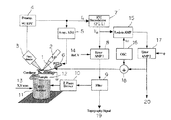
図3において、カンチレバー1の背面には、光源2からのレーザー光が照射され、その反射光は、光検出器3により検出される。この光てこ方式によりカンチレバー1の振動変位が検出され、バンドパスフィルタが内蔵されたプリアンプ4により電気的に増幅される。電気信号に変換されたカンチレバー1の変位信号は、アッテネータ5を介して加振用PZT6に入力されるループが組まれている。
図示していないが、このループには、フェーズシフタも組み込まれており、カンチレバー1の固有振動数で正帰還発振するように設定されている。アッテネータ5では、AGC等によりカンチレバー1の振動振幅、あるいは加振用PZT6に入力される電圧振幅が一定になるように制御されている。
【0005】
発振波形は途中分岐されて、PLL(Phased Lock Loop) で構成されているFMデモジュレータ7に入力され、その発振周波数f0 に相当する電圧Vf0に変換して出力する(f/V変換;f0 からVf0に変換)。探針・試料間に作用する力の勾配Fとバネ定数kのカンチレバー1の固有振動数f0 には、
f0 ∝√(k−F)
の関係があり、f0 の変化(周波数シフト)はほぼFに相当する。f/V変換された周波数に相当する信号は、誤差増幅器8によりその周波数が固有振動数からある一定量シフトするようにフィルタ9、Zピエゾドライバ10を介してPZTスキャナ11のZ動が制御される(フィードバック1)。
【0006】
一定に保持される周波数シフトは、基準電圧(Ref.V)14によって設定される。この時のZ動を制御している信号(フィルタ9の出力)が表面の凹凸(トポグラフィ信号)に相当し、スキャン信号(X,Yスキャン13)によりPZTスキャナ11が2次元的にスキャンされ、その時のZ動を輝度信号とすることでTopo像が得られる。
【0007】
カンチレバー1の固有振動数f0 は、探針・試料間の静電気力によってもシフトする。導電性のカンチレバー1にオシレータ16及び誤差増幅器17からの電圧[VDC+VACsin(ωt)]を印加した場合、接地された試料12と探針(カンチレバー1)との間に電位差が生じ静電気力が作用する。印加電圧の交流成分の周波数がFMデモジュレータ7の動作帯域より小さく、且つフィードバック1の帯域を越えた値(追従できない値)に設定されれば、FMデモジュレータ7の出力Vf0にその交流成分による変調が現れる。この信号をロックインアンプ15で、ωを参照信号として検出すると、ω成分の振幅に相当する出力が得られる。この出力がゼロのときカンチレバー(探針)・試料間の静電気力が最小となり、この状態を維持するように直流電圧VDCが誤差増幅器17から加算器18を経て、カンチレバー(探針)1の電位としてフィードバックされる(フィードバック2)。このVDCが探針に対する試料表面のCPDであり、試料表面のTopo信号と同時に表示することで、NC−AFM像19と電位像20が同時観察される。
【0008】
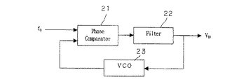
FMデモジュレータ7であるPLLは、図4に示すように位相比較器21とフィルタ22とVCO(Voltage Control Oscilator)23から構成されている。カンチレバー1の固有周波数付近の発振信号を制御できるように設定されているVCO23からの発振波形と、カンチレバー1の固有振動数で発振している信号f0 は、位相比較器21に入力され、その位相信号は、フィルタ効果が大きい(時定数が大きい)フィルタ22を介してVCO23の制御信号となる。このループは、常に位相差がゼロとなるようなフィードバックループとなる。フィルタ22の出力が一般にNC−AFMでの周波数シフト信号として用いられるため、周波数の変化をより高感度に検出でき、且つこのフィードバックループを安定に働かせるためにフィルタ22は、フィルタ効果が大きい(時定数が大きい)定数を選ぶ必要がある。
【0009】
【特許文献1】
特開平11−23588号公報
【0010】
【発明が解決しようとする課題】
f/V変換に使用されているPLL内のフィルタ22は、周波数の変化をより高感度で検出でき、且つこのフィードバックループを安定に働かせるために、比較的時定数の大きなフィルタが用いられているので、結果としてf/V変換の帯域を数kHzまで落とすことになる。そのため、SKPMによる静電気力等のNC−AFMのフィードバック信号に重畳させTopo像と同時に他の物理量をロックインアンプを用いて検出する場合、その変調周波数がf/V変換の帯域に制限され、より利得を稼ぐための高周波数変調ができない。
【0011】
【課題を解決するための手段】
本発明は、上記課題を解決するものであって、NC−AFM像と電位像の同時観察において高感度での周波数の変化の検出と検出利得の向上を図るものである。
【0012】
そのために本発明は、探針を先端に有し該探針が試料の表面に近接配置されるカンチレバーと、前記試料と前記探針とを相対的にX,Yスキャンするスキャン手段と、前記試料と前記探針との距離を相対的に変化させるZ動駆動手段と、前記カンチレバーの振動変位を検出する変位検出手段と、該変位検出手段の検出信号により前記カンチレバーを固有振動数で正帰還発振させる加振手段とを備え、前記変位検出手段の検出信号をZ動駆動手段にフィードバックすると共に前記カンチレバーと試料との間の電位値としてフィードバックすることにより、非接触原子間力顕微鏡像と電位像を観察できるようにした試料表面観察装置において、前記変位検出手段の検出信号を入力とする位相比較器を有し周波数シフトを電圧に変換して周波数が前記カンチレバーの固有振動数より一定量シフトするように前記Z動駆動手段をZ動駆動する第1のフィードバック手段と、前記第1のフィードバック手段の位相比較器の出力を直接取り出してフィルタを介してロックイン検出し前記カンチレバーと試料との間の電位差としてフィードバックする第2のフィードバック手段とを備えたことを特徴とするものである。
【0013】
【発明の実施の形態】
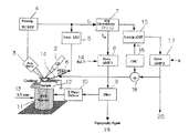
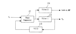
以下、本発明の実施の形態を図面を参照しつつ説明する。図1は本発明に係る試料表面観察装置の実施の形態を示す図、図2は本発明に係る試料表面観察装置のFMデモジュレータを構成するPLLの実施の形態を示す図である。図中、1はカンチレバー、2は光源、3は光検出器、4はプリアンプ、5はアッテネータ、6は加振用PZT、7はFMデモジュレータ、8、17は誤差増幅器、9、22、24はフィルタ、10はピエゾドライバ、11はPZTスキャナ、12は試料、13はX,Yスキャン、14は基準電圧、15はロックインアンプ、16はオシレータ、18は加算器、19はNC−AFM像、20は電位像、21は位相比較器、23はVCOを示す。
【0014】
図1において、カンチレバー1は、探針を先端に有しその探針が試料12の表面に近接配置され、その背面には、光源(LD)2からのレーザー光が照射され、その反射光は、光検出器(PD)3により検出される。この光てこ方式の振動変位検出手段によりカンチレバー1の振動変位が検出され、バンドパスフィルタが内蔵されたプリアンプ4により電気的に増幅される。電気信号に変換されたカンチレバー1の変位信号は、アッテネータ5を介して加振用PZT6に入力されるループが組まれている。図示していないが、このループには、フェーズシフタも組み込まれており、カンチレバー1の固有振動数で正帰還発振するように設定されている。アッテネータ5では、AGC等によりカンチレバー1の振動振幅、あるいは加振用PZT6に入力される電圧振幅が一定になるように制御されている。
【0015】
電気信号に変換されたカンチレバー1の発振波形は途中分岐されて、PLLで構成されているFMデモジュレータ7に入力され、その発振周波数f0 に相当する電圧Vf0に変換して出力する。探針・試料間に作用する力の勾配Fとバネ定数kのカンチレバー1の固有振動数f0 には、
f0 ∝√(k−F)
の関係があり、f0 の変化(周波数シフト)はほぼFに相当する。f/V変換された周波数に相当する信号は、誤差増幅器8によりその周波数が固有振動数からある一定量シフトするようにフィルタ9、Zピエゾドライバ10を介してPZTスキャナ11のZ動が制御される(第1のフィードバック手段)。
【0016】
一定に保持される周波数シフトは、基準電圧(Ref.V)14によって設定される。この時のZ動を制御している信号(フィルタ9の出力)が表面の凹凸(トポグラフィ信号)に相当し、スキャン信号(X,Yスキャン13)によりPZTスキャナ11が2次元的にスキャンされ、その時のZ動を輝度信号とすることでTopo像が得られる。PZTスキャナ11は、接地された試料12をX,Yスキャン及びZ動駆動するスキャン手段である。
【0017】
カンチレバー1の固有振動数f0 は、探針・試料間の静電気力によってもシフトする。導電性のカンチレバー1にオシレータ16及び誤差増幅器17からの電圧[VDC+VACsin(ωt)]を印加した場合、試料12と探針(カンチレバー1)との間に電位差が生じ静電気力が作用する。FMデモジュレータ7の位相比較器21の動作帯域は、カンチレバー1の固有振動数(数100kHz)より十分大きいため、印加電圧の交流成分の周波数は、カンチレバー1の固有振動数より小さく、且つフィードバック1の帯域を越えた値(追従できない値)に設定されれば、位相比較器21の出力Vf0にその交流成分による変調が含まれる。この信号をロックインアンプ15で、ωを参照信号として検出すると、ω成分の振幅に相当する出力が得られる。この出力がゼロのときカンチレバー1の探針・試料間の静電気力が最小となり、この状態を維持するように直流電圧VDCが誤差増幅器17から加算器18を経て、カンチレバー1の探針の電位としてフィードバックされる(第2のフィードバック手段)。このVDCが探針に対する試料表面のCPDであり、試料表面のTopo信号と同時に表示することで、NC−AFM像19と電位像20が同時観察される。
【0018】
本実施形態におけるPLLは、図2に示すように位相比較器21、フィルタ22、VCO23からなるPLLとしてのフィードバックループは従来のものと同じであるが、位相比較器21の出力から重畳信号検出用の出力を取り出している。その出力には、必要に応じてフィルタ24を設ける。この出力を図1に示すロックインアンプ15の入力に接続することにより、従来より高利得で電位信号が検出でき、その結果電位分解能が向上したNC−AFM像19と電位像20が同時観察できるようにしている。
【0019】
本実施形態では、このようにFMデモジュレータ7、誤差増幅器8、フィルタ8、Zピエゾドライバ10からなる第1のフィードバック手段において、変位検出手段(2〜4)の検出信号を入力とするFMデモジュレータ7の位相比較器21、フィルタ22で周波数シフトを電圧に変換して周波数がカンチレバー1の固有振動数より一定量シフトするようにスキャン手段のPZTスキャナ11をZ動制御している。そして、ロックインアンプ15、オシレータ16、誤差増幅器17、加算器18からなる第2のフィードバック手段において、第1のフィードバック手段の位相比較器21の出力を直接取り出してフィルタ24を介してロックイン検出しカンチレバー1の電位にフィードバックしている。
【0020】
なお、本発明は、上記実施の形態に限定されるものではなく、種々の変形が可能である。例えば上記実施の形態では、PZTスキャナにより2次元的にX,Yスキャンすると共に、Z動駆動を行うようにしたが、スキャン手段により試料と探針とを相対的にX,Yスキャンし、別に試料と探針との距離を相対的に変化させるZ動駆動手段を設ける構成としてもよい。
【0021】
【発明の効果】
以上の説明から明らかなように、本発明によれば、NC−AFMの画像信号であるカンチレバーの固有振動数の周波数シフト信号に重畳させ、その後段でロックイン検出していた静電気力等の信号検出において、周波数シフトを電圧変換するPLL内でその帯域を制限していたフィルタを通さない信号、すなわち位相比較器の出力を直接ロックイン検出することで重畳信号の変調周波数を高くすることができ、その検出利得を向上させることができる。また、位相比較器の出力を直接取り出しPLL内のフィルタよりフィルタ効果の小さいフィルタを介してロックイン検出することで重畳信号の変調周波数を高くすることができ、その検出利得の向上を図ることができる。
【図面の簡単な説明】
【図1】本発明に係る試料表面観察装置の実施の形態を示す図である。
【図2】本発明に係る試料表面観察装置のFMデモジュレータを構成するPLLの実施の形態を示す図である。
【図3】従来の試料表面観察装置の構成例を示す図である。
【図4】FMデモジュレータとして用いるPLLの構成例を示す図である。
【符号の説明】
1…カンチレバー、2…光源、3…光検出器、4…プリアンプ、5…アッテネータ、6…加振用PZT、7…FMデモジュレータ、8、17…誤差増幅器、9、22、24…フィルタ、10…ピエゾドライバ、11…PZTスキャナ、12…試料、13…X,Yスキャン、14…基準電圧、15…ロックインアンプ、16…オシレータ、18…加算器、19…NC−AFM像、20…電位像、21…位相比較器、23…VCO[0001]
TECHNICAL FIELD OF THE INVENTION
According to the present invention, there is provided a cantilever having a probe at a tip thereof, the probe being disposed close to the surface of a sample, a scanning unit for performing X and Y scans relative to the sample and the probe, Z movement drive means for relatively changing the distance, displacement detection means for detecting the vibration displacement of the cantilever, and vibration means for positively oscillating the cantilever at a natural frequency by a detection signal of the displacement detection means, A sample surface observing apparatus that enables a non-contact atomic force microscope image and an electric potential image to be observed by feeding back a detection signal of the displacement detecting means to the Z-motion driving means and feeding back a potential value between the cantilever and the sample. About.
[0002]
[Prior art]
One of SPM (Scanning Probe Microscope: Scanning Probe Microscope), in which NC-AFM (Noncontact Atomic Force Microscope: Non-Contact Atomic Force Microscope) technology is applied, and SKPM (Scanning Kelvin Probe Kombin Probe Micro Force Probe Microscope) As a device related to a microscope, etc., there is a surface observation device for observing a potential distribution or the like on a sample surface (for example, see Patent Document 1). In SKPM and the like, signals such as electrostatic force to be simultaneously detected are superimposed on an NC-AFM feedback signal which is a main signal. In the detection, a Slope detection method is used in the atmosphere, but an FM detection method is used in a vacuum. It is common.
[0003]
FIG. 3 is a diagram illustrating a configuration example of a conventional sample surface observation device, and FIG. 4 is a diagram illustrating a configuration example of a PLL used as an FM demodulator.
[0004]
3, the back surface of the
Although not shown, a phase shifter is also incorporated in this loop, and the loop is set so as to perform positive feedback oscillation at the natural frequency of the
[0005]
Oscillation waveform is branched midway, PLL is input to the FM demodulator 7 which is composed of (Phased Lock Loop), the oscillation frequency f 0 is converted into a voltage V f0 corresponding to outputting (f / V conversion; conversion from f 0 to V f0). The natural frequency f 0 of the
f 0 ∝√ (k-F)
The change of f 0 (frequency shift) substantially corresponds to F. The Z-movement of the
[0006]
The frequency shift kept constant is set by the reference voltage (Ref. V) 14. The signal controlling the Z movement (output of the filter 9) at this time corresponds to the surface unevenness (topography signal), and the
[0007]
Natural frequency f 0 of the
[0008]
The PLL as the FM demodulator 7 includes a
[0009]
[Patent Document 1]
JP-A-11-23588
[Problems to be solved by the invention]
As the
[0011]
[Means for Solving the Problems]
The present invention solves the above-described problems, and aims to detect a change in frequency with high sensitivity and improve a detection gain in simultaneous observation of an NC-AFM image and a potential image.
[0012]
For this purpose, the present invention provides a cantilever having a probe at a tip thereof, the probe being disposed close to the surface of a sample, a scanning unit for performing X and Y scans relative to the sample and the probe, Driving means for relatively changing the distance between the cantilever and the probe, displacement detecting means for detecting a vibration displacement of the cantilever, and positive feedback oscillation of the cantilever at a natural frequency by a detection signal of the displacement detecting means. And a feedback signal as a potential value between the cantilever and the sample by feeding back the detection signal of the displacement detecting means to the Z-motion driving means, thereby providing a non-contact atomic force microscope image and a potential image. In the sample surface observation apparatus which can observe the frequency, the apparatus has a phase comparator which receives the detection signal of the displacement detecting means as an input, and converts the frequency shift into a voltage so that the frequency is First feedback means for Z-moving the Z-movement driving means so as to shift by a certain amount from the natural frequency of the cantilever, and the output of the phase comparator of the first feedback means is directly taken out and locked via a filter. Second feedback means for detecting in-feed and feeding back as a potential difference between the cantilever and the sample.
[0013]
BEST MODE FOR CARRYING OUT THE INVENTION
Hereinafter, embodiments of the present invention will be described with reference to the drawings. FIG. 1 is a diagram showing an embodiment of a sample surface observation device according to the present invention, and FIG. 2 is a diagram showing an embodiment of a PLL constituting an FM demodulator of the sample surface observation device according to the present invention. In the figure, 1 is a cantilever, 2 is a light source, 3 is a photodetector, 4 is a preamplifier, 5 is an attenuator, 6 is a PZT for excitation, 7 is an FM demodulator, 8, 17 are error amplifiers, 9, 22, and 24. Is a filter, 10 is a piezo driver, 11 is a PZT scanner, 12 is a sample, 13 is an X and Y scan, 14 is a reference voltage, 15 is a lock-in amplifier, 16 is an oscillator, 18 is an adder, and 19 is an NC-AFM image. , 20 are potential images, 21 is a phase comparator, and 23 is a VCO.
[0014]
In FIG. 1, a
[0015]
The oscillation waveform of the
f 0 ∝√ (k-F)
The change of f 0 (frequency shift) substantially corresponds to F. The Z-movement of the
[0016]
The frequency shift kept constant is set by the reference voltage (Ref. V) 14. The signal controlling the Z movement (output of the filter 9) at this time corresponds to the surface unevenness (topography signal), and the
[0017]
Natural frequency f 0 of the
[0018]
The PLL in the present embodiment has the same feedback loop as a conventional PLL including a
[0019]
In the present embodiment, in the first feedback means including the FM demodulator 7, the error amplifier 8, the filter 8, and the Z
[0020]
Note that the present invention is not limited to the above embodiment, and various modifications are possible. For example, in the above-described embodiment, the X and Y scans are performed two-dimensionally by the PZT scanner, and the Z movement drive is performed. A configuration may be adopted in which a Z-motion drive unit that relatively changes the distance between the sample and the probe is provided.
[0021]
【The invention's effect】
As is clear from the above description, according to the present invention, the signal such as the electrostatic force which is superimposed on the frequency shift signal of the natural frequency of the cantilever, which is the image signal of the NC-AFM, and lock-in is detected in the subsequent stage. In the detection, the modulation frequency of the superimposed signal can be increased by directly performing lock-in detection of a signal that does not pass through a filter whose band has been limited in a PLL that converts a frequency shift into a voltage, that is, a phase comparator output. , The detection gain can be improved. Further, by directly taking out the output of the phase comparator and performing lock-in detection through a filter having a smaller filter effect than the filter in the PLL, the modulation frequency of the superimposed signal can be increased, and the detection gain can be improved. it can.
[Brief description of the drawings]
FIG. 1 is a diagram showing an embodiment of a sample surface observation device according to the present invention.
FIG. 2 is a diagram showing an embodiment of a PLL constituting an FM demodulator of the sample surface observation device according to the present invention.
FIG. 3 is a diagram showing a configuration example of a conventional sample surface observation device.
FIG. 4 is a diagram illustrating a configuration example of a PLL used as an FM demodulator;
[Explanation of symbols]
DESCRIPTION OF
Claims (1)
Priority Applications (1)
| Application Number | Priority Date | Filing Date | Title |
|---|---|---|---|
| JP2003014467A JP4146251B2 (en) | 2003-01-23 | 2003-01-23 | Sample surface observation equipment |
Applications Claiming Priority (1)
| Application Number | Priority Date | Filing Date | Title |
|---|---|---|---|
| JP2003014467A JP4146251B2 (en) | 2003-01-23 | 2003-01-23 | Sample surface observation equipment |
Publications (2)
| Publication Number | Publication Date |
|---|---|
| JP2004226237A true JP2004226237A (en) | 2004-08-12 |
| JP4146251B2 JP4146251B2 (en) | 2008-09-10 |
Family
ID=32902512
Family Applications (1)
| Application Number | Title | Priority Date | Filing Date |
|---|---|---|---|
| JP2003014467A Expired - Fee Related JP4146251B2 (en) | 2003-01-23 | 2003-01-23 | Sample surface observation equipment |
Country Status (1)
| Country | Link |
|---|---|
| JP (1) | JP4146251B2 (en) |
Cited By (5)
| Publication number | Priority date | Publication date | Assignee | Title |
|---|---|---|---|---|
| WO2008029562A1 (en) | 2006-09-04 | 2008-03-13 | National University Corporation Kanazawa University | Atomic force microscope |
| JP2008058107A (en) * | 2006-08-30 | 2008-03-13 | Seiko Instruments Inc | Potential difference detection method and scanning probe microscope |
| WO2010023811A1 (en) | 2008-08-28 | 2010-03-04 | 国立大学法人 金沢大学 | Scanning type probe microscope |
| JP2010066140A (en) * | 2008-09-11 | 2010-03-25 | Jeol Ltd | Scanning probe microscope |
| JP2011053018A (en) * | 2009-08-31 | 2011-03-17 | Tdk Corp | Method and device for measuring potential in liquid |
Families Citing this family (1)
| Publication number | Priority date | Publication date | Assignee | Title |
|---|---|---|---|---|
| JP6696570B2 (en) * | 2016-06-02 | 2020-05-20 | 株式会社島津製作所 | Scanning probe microscope |
-
2003
- 2003-01-23 JP JP2003014467A patent/JP4146251B2/en not_active Expired - Fee Related
Cited By (8)
| Publication number | Priority date | Publication date | Assignee | Title |
|---|---|---|---|---|
| JP2008058107A (en) * | 2006-08-30 | 2008-03-13 | Seiko Instruments Inc | Potential difference detection method and scanning probe microscope |
| US7861577B2 (en) | 2006-08-30 | 2011-01-04 | Seiko Instruments Inc. | Electric potential difference detection method and scanning probe microscope |
| WO2008029562A1 (en) | 2006-09-04 | 2008-03-13 | National University Corporation Kanazawa University | Atomic force microscope |
| US7975315B2 (en) | 2006-09-04 | 2011-07-05 | National University Corporation Kanazawa University | Atomic force microscope |
| WO2010023811A1 (en) | 2008-08-28 | 2010-03-04 | 国立大学法人 金沢大学 | Scanning type probe microscope |
| US8387159B2 (en) | 2008-08-28 | 2013-02-26 | National University Corporation | Scanning type probe microscope |
| JP2010066140A (en) * | 2008-09-11 | 2010-03-25 | Jeol Ltd | Scanning probe microscope |
| JP2011053018A (en) * | 2009-08-31 | 2011-03-17 | Tdk Corp | Method and device for measuring potential in liquid |
Also Published As
| Publication number | Publication date |
|---|---|
| JP4146251B2 (en) | 2008-09-10 |
Similar Documents
| Publication | Publication Date | Title |
|---|---|---|
| US6005246A (en) | Scanning probe microscope | |
| US8387159B2 (en) | Scanning type probe microscope | |
| JPH1130619A (en) | Scanning probe microscope | |
| JP2002107285A (en) | Magnetic force microscope | |
| US6845655B2 (en) | Heterodyne feedback system for scanning force microscopy and the like | |
| JP4851375B2 (en) | Phase feedback AFM control method and phase feedback AFM | |
| US8726409B2 (en) | Method for driving a scanning probe microscope at elevated scan frequencies | |
| JPH11160333A (en) | Scanning probe microscope | |
| JP4496350B2 (en) | Atomic force microscope | |
| JP4913242B2 (en) | Dynamic mode AFM device | |
| JP2002310882A (en) | Signal detection device using scanning probe, probe microscope using the device, signal detection method using scanning probe, observation method for observing sample surface using the method | |
| JP4146251B2 (en) | Sample surface observation equipment | |
| JP4474556B2 (en) | Scanning probe microscope | |
| JP4111867B2 (en) | Scanning probe microscope | |
| JP4027809B2 (en) | Sample surface shape observation equipment | |
| JP2003194699A (en) | Signal detector and non-contact atomic force microscope using the signal detector | |
| US8087289B2 (en) | High resolution surface potential microscope | |
| JP3453277B2 (en) | Scanning probe microscope | |
| JP2009092499A (en) | Atomic force microscope approach control method and apparatus | |
| JP2003185555A (en) | Frequency detection method and scanning probe microscope using the same | |
| WO2011040065A1 (en) | Scanning probe microscope | |
| JP4943822B2 (en) | Scanning probe microscope | |
| JP2000227436A (en) | Scanning probe microscope, and method for observating sample |
Legal Events
| Date | Code | Title | Description |
|---|---|---|---|
| A621 | Written request for application examination |
Free format text: JAPANESE INTERMEDIATE CODE: A621 Effective date: 20050712 |
|
| A977 | Report on retrieval |
Free format text: JAPANESE INTERMEDIATE CODE: A971007 Effective date: 20070312 |
|
| A131 | Notification of reasons for refusal |
Free format text: JAPANESE INTERMEDIATE CODE: A131 Effective date: 20080319 |
|
| A521 | Written amendment |
Free format text: JAPANESE INTERMEDIATE CODE: A523 Effective date: 20080519 |
|
| TRDD | Decision of grant or rejection written | ||
| A01 | Written decision to grant a patent or to grant a registration (utility model) |
Free format text: JAPANESE INTERMEDIATE CODE: A01 Effective date: 20080611 |
|
| A01 | Written decision to grant a patent or to grant a registration (utility model) |
Free format text: JAPANESE INTERMEDIATE CODE: A01 |
|
| A61 | First payment of annual fees (during grant procedure) |
Free format text: JAPANESE INTERMEDIATE CODE: A61 Effective date: 20080619 |
|
| R150 | Certificate of patent or registration of utility model |
Free format text: JAPANESE INTERMEDIATE CODE: R150 |
|
| FPAY | Renewal fee payment (event date is renewal date of database) |
Free format text: PAYMENT UNTIL: 20110627 Year of fee payment: 3 |
|
| FPAY | Renewal fee payment (event date is renewal date of database) |
Free format text: PAYMENT UNTIL: 20120627 Year of fee payment: 4 |
|
| FPAY | Renewal fee payment (event date is renewal date of database) |
Free format text: PAYMENT UNTIL: 20120627 Year of fee payment: 4 |
|
| FPAY | Renewal fee payment (event date is renewal date of database) |
Free format text: PAYMENT UNTIL: 20130627 Year of fee payment: 5 |
|
| FPAY | Renewal fee payment (event date is renewal date of database) |
Free format text: PAYMENT UNTIL: 20130627 Year of fee payment: 5 |
|
| LAPS | Cancellation because of no payment of annual fees |