JP2004228296A - Air core coil - Google Patents
Air core coil Download PDFInfo
- Publication number
- JP2004228296A JP2004228296A JP2003013517A JP2003013517A JP2004228296A JP 2004228296 A JP2004228296 A JP 2004228296A JP 2003013517 A JP2003013517 A JP 2003013517A JP 2003013517 A JP2003013517 A JP 2003013517A JP 2004228296 A JP2004228296 A JP 2004228296A
- Authority
- JP
- Japan
- Prior art keywords
- conductor
- coil
- substrate
- substrate opening
- insulating substrate
- Prior art date
- Legal status (The legal status is an assumption and is not a legal conclusion. Google has not performed a legal analysis and makes no representation as to the accuracy of the status listed.)
- Pending
Links
Images



Landscapes
- Coils Or Transformers For Communication (AREA)
Abstract
【課題】測定誤差が小さく、また作製が容易な空芯コイルを得ることを目的とする。
【解決手段】空芯コイルは、絶縁性基板2と、この絶縁性基板2に設けられたコイル本体3とを備えている。絶縁性基板2は基板開口部4を有している。コイル本体3は、絶縁性基板2に付着された導電膜である。絶縁性基板2の表面8及び裏面9には、溝部20が形成され、溝部20の内面に導電膜が付着されている。コイル本体3は、絶縁性基板2の全面に付着された導電膜をポリッシングにより一部除去して各溝部20内に残すことにより形成される。各溝部20間の仕切部21は、先端部22に形成された平面23の幅W1が基部24の幅W2よりも小さくなっている。
【選択図】 図4An object of the present invention is to obtain an air-core coil which has a small measurement error and is easy to manufacture.
An air-core coil includes an insulating substrate (2) and a coil body (3) provided on the insulating substrate (2). The insulating substrate 2 has a substrate opening 4. The coil main body 3 is a conductive film attached to the insulating substrate 2. A groove 20 is formed on the front surface 8 and the back surface 9 of the insulating substrate 2, and a conductive film is attached to the inner surface of the groove 20. The coil body 3 is formed by removing a part of the conductive film attached to the entire surface of the insulating substrate 2 by polishing and leaving the conductive film in each groove 20. In the partition 21 between the grooves 20, the width W1 of the plane 23 formed on the distal end 22 is smaller than the width W2 of the base 24.
[Selection diagram] Fig. 4
Description
【0001】
【発明の属する技術分野】
この発明は、例えば被測定導体を流れるインパルス大電流等を測定する電流センサに用いられる空芯コイルに関するものである。
【0002】
【従来の技術】
空芯コイルは、巻芯に鉄心等の強磁性体を有しないコイルであり、磁気飽和にならない性質がある。従って、空芯コイルを被測定導体に流れる電流測定のための電流センサに用いると、幅広い電流範囲の測定が可能となる。また、電流センサの空芯コイルには、外部電磁界による測定誤差を抑制するためにロゴスキーコイルが用いられる。ロゴスキーコイルは、導線がソレノイド状に巻き進められ、その巻き終わりから巻き始めまで戻されて構成されたコイルである。
【0003】
従来のロゴスキーコイルは、平面プリント回路板に金を堆積させて構成されている。このロゴスキーコイルは、平面プリント回路板に構成されているので、ほとんど完全に軸方向に対称に作製できる(例えば、特許文献1参照)。
【0004】
【特許文献1】
特開平6−176947号公報
【0005】
【発明が解決しようとする課題】
このように従来の空芯コイルを作製する場合、平面プリント回路板に金堆積物をパターン配置する必要があるので手間がかかる。
また、従来の空芯コイルを電流センサに用いる場合、被測定導体の軸周りに沿って見たときに、ロゴスキーコイルの巻き進みコイルによって囲まれる面積と巻き戻しコイルによって囲まれる面積とが異なっているので、それぞれに発生する誘導起電力の大きさに差が生じ、測定誤差が大きくなる。
【0006】
そこでこの発明は、上記のような問題点を解決することを課題とするもので、測定誤差が小さく、また作製が容易な空芯コイルを得ることを目的とする。
【0007】
【課題を解決するための手段】
この発明に係る空芯コイルは、表面と、裏面と、表面及び裏面を貫通し、被測定導体が通される基板開口部とを有する絶縁性基板、表面及び裏面での基板開口部の周囲で略放射状に設けられた複数の導体部と、表面の各導体部及び裏面の各導体部のそれぞれの端部に接続された複数の接続導体部とを有し、各導体部及び各接続導体部によりコイル状に構成されたコイル本体を備え、表面及び裏面の少なくとも一方には、基板開口部の周囲で略放射状に延びる複数の溝部と複数の仕切部とが交互に配列され、導体部が各溝部にそれぞれ設けられており、仕切部の先端部の幅は、仕切部の基部の幅よりも小さくなっている。
【0008】
【発明の実施の形態】
以下、この発明の実施の形態を図面を参照しながら説明する。
実施の形態1.
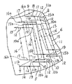
図1は、この発明の実施の形態1による空芯コイルを示す正面図であり、図2は、図1の接続点7付近のコイル本体3を示す部分拡大図である。図において、空芯コイル1は、樹脂等の非磁性体で作製された絶縁性基板2と、この絶縁性基板2に設けられたコイル本体3とを備えている。絶縁性基板2は、被測定導体が通される円形状の基板開口部4を中央に有した円板である。コイル本体3は、基板開口部4の外周に沿って導線が巻回されるように形成された巻き進みコイル部5及び巻き戻しコイル部6を有している。
【0009】
巻き進みコイル部5と巻き戻しコイル部6とは接続点7で電気的に直列に接続されている。巻き進みコイル部5及び巻き戻しコイル部6のそれぞれの導線には、被測定導体に流れる電流に対応した誘導起電力が発生するようになっている。巻き進みコイル部5及び巻き戻しコイル部6は、この誘導起電力が電気的に同じ向きになるように巻回されている。また、巻き進みコイル部5及び巻き戻しコイル部6を構成する導線は、絶縁性基板2にコイル状に付着された銅の導電膜である。
即ち、空芯コイル1は、導体が巻き進められた巻き進みコイル部5と、巻き進みコイル部5の終端部に接続されて導線が巻き進みコイル部5に沿って巻き戻された巻き戻しコイル部6とから構成されるロゴスキーコイルである。
【0010】
絶縁性基板2には、コイル本体3の引出部30、31に電気的に接続された信号処理回路32が取り付けられている。信号処理回路32は、コイル本体3に発生する誘導電流を積分処理する回路である。誘導電流は、被測定導体に流れる電流波形の微分値としてコイル本体3に発生し、信号処理回路32の積分処理により被測定導体の電流波形が復元される。
【0011】
絶縁性基板2の表面8及び裏面9には、導電膜である複数の第1表面導体部10(導体部)及び導電膜である複数の第1裏面導体部11(導体部)がそれぞれ付着されている。また、絶縁性基板2には、絶縁性基板2を貫通する複数の接続導体部12が設けられている。巻き進みコイル部5は、複数の第1表面導体部10及び複数の第1裏面導体部11が各接続導体部12を介して電気的に直列に接続されてコイル状に形成されたものである。
【0012】
絶縁性基板2の表面8及び裏面9にはまた、導電膜である複数の第2表面導体部15(導体部)及び導電膜である複数の第2裏面導体部16(導体部)がそれぞれ付着されている。各第2表面導体部15は、各第1表面導体部10の間に配置され、各第2裏面導体部16は、各第1裏面導体部11の間に配置されている。また、絶縁性基板2には、絶縁性基板2を貫通する複数の接続導体部17が設けられている。巻き戻しコイル部6は、複数の第2表面導体部15及び複数の第2裏面導体部16が各接続導体部17を介して電気的に直列に接続されてコイル状に形成されたものである。なお、図1及び図2において、裏面9に形成された導電膜は、破線で示している。
【0013】
各第1表面導体部10は、内側端部10aが基板開口部4に近い側に配置され、外側端部10bが基板開口部4から遠い側に配置されるように、基板開口部4の周囲で略放射状に一定ピッチでそれぞれ配列されている。
【0014】
各第1裏面導体部11は、接続導体部12への接続のために基板開口部4から離れた側でそれぞれ屈曲されている。また、各第1裏面導体部11は、内側端部11aが基板開口部4に近い側に配置され、外側端部11bが基板開口部4から遠い側に配置されるように、基板開口部4の周囲で略放射状に一定ピッチで配列されている。
【0015】
各第2表面導体部15は、表面8で基板開口部4の周囲に略放射状に第1表面導体部10と交互になるように一定ピッチで配列されている。また、各第2表面導体部15は、各内側端部15a及び各外側端部15bがそれぞれ各内側端部10a及び各外側端部10bよりも基板開口部4に近い位置になるように配置されている。
【0016】
各第2裏面導体部16は、接続導体部17への接続のために基板開口部4に近い側で屈曲されている。また、各第2裏面導体部16は、裏面9で基板開口部4の周囲に略放射状に第1裏面導体部11と交互になるように一定ピッチで配列されている。また、各第2裏面導体部16は、各内側端部16a及び各外側端部16bがそれぞれ各内側端部11a及び各外側端部11bよりも基板開口部4に近い位置になるように配置されている。
【0017】
図1に示すように、各第1表面導体部10及び第1裏面導体部11の略放射状部分は互いに対向されて配置され、各第2表面導体部15及び第2裏面導体部16の略放射状部分は互いに対向されて配置されている。
各第1表面導体部10及び各第1裏面導体部11は、絶縁性基板2の厚さ方向に沿って見たとき、各内側端部10aと各内側端部11aとが重なり、各外側端部10bと各外側端部11bとが重なるように配列されている。また、各第2表面導体部15及び各第2裏面導体部16は、絶縁性基板2の厚さ方向に沿って見たとき、各内側端部15aと各内側端部16aとが重なり、各外側端部15bと各外側端部16bとが重なるように配列されている。なお、図1においては、分かり易くするために、互いに対向する略放射状部分を並べて示している。
【0018】
接続導体部12は、図1において互いに重なる各内側端部10a及び11aを電気的に接続する複数の第1内側接続導体部13と、図1において互いに重なる各外側端部10b及び11bを電気的に接続する複数の第1外側接続導体部14とからなっている。
【0019】
接続導体部17は、各内側端部15a及び各内側端部16aを電気的に接続する複数の第2内側接続導体部18と、各外側端部15b及び各外側端部16bを電気的に接続する複数の第2外側接続導体部19とからなっている。
【0020】
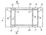
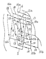
図3は、図1の基板開口部4の外周に沿って(図1の矢印27の向きに沿って)見たときの絶縁性基板2、巻き進みコイル部5及び巻き戻しコイル部6を示す配置図である。図において、絶縁性基板2の表面8及び裏面9には、複数の溝部20がそれぞれ形成されている。各溝部20は、基板開口部4の周囲で略放射状に延びており、基板開口部4の周方向に沿って配列されている。第1表面導体部10、第1裏面導体部11、第2表面導体部15及び第2裏面導体部16は、各溝部20の内面に付着されている。
また、接続導体部12及び接続導体部17は、絶縁性基板2の厚さ方向に沿って絶縁性基板2を貫通する貫通孔の内面に形成された銅の導電膜、即ち金属スルーホールである。
【0021】
また、第2内側接続導体部18は、第1内側接続導体部13よりも基板開口部4に近い側に配置され、第2外側接続導体部19は、第1外側接続導体部14よりも基板開口部4に近い側、かつ第1内側接続導体部13よりも基板開口部4から遠い側に配置されている。
【0022】
即ち、巻き進みコイル部5及び巻き戻しコイル部6は、基板開口部4の外周に沿って見たときに、巻き進みコイル部5の導線によって囲まれる領域、即ち第1表面導体部10、第1裏面導体部11、第1内側接続導体部13及び第1外側接続導体部14によって囲まれる領域(以下、巻き進みコイル部5の断面領域という)と、巻き戻しコイル部6の導線によって囲まれる領域、即ち第2表面導体部15、第2裏面導体部16、第2内側接続導体部18及び第2外側接続導体部19によって囲まれる領域(以下、巻き戻しコイル部6の断面領域という)とが、大部分で互いに重なって配置されている。さらに、巻き進みコイル部5の断面領域の面積と巻き戻しコイル部6の断面領域の面積とがほぼ同一となっている。
【0023】
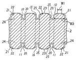
図4は、図3のIV−IV線に沿った断面図である。図において、互いに隣接する溝部20の間には、仕切部21が形成されている。仕切部21は、各溝部20の形成により絶縁性基板2の一部が残されて形成されたものである。各仕切部21の先端部22には、絶縁性基板2の厚さ方向に対して垂直な平面23がそれぞれ形成されている。平面23の幅W1は、その仕切部21の基部24の幅W2よりも小さくなっている。即ち、平面23の溝部20の配列方向に沿った幅W1は、基部24の溝部20の配列方向に沿った幅W2よりも小さくなっている。ここでは、各溝部20の解放側が広げられて仕切部21の先端部22にテーパ面25が形成されることにより、各溝部20の底部に隣接した基部24の幅W2よりも小さい幅W1の平面23が形成されている。平面23には、導電膜は付着されていない。従って、互いに隣り合う溝部20に付着された導電膜、即ち第1表面導体部10及び第2表面導体部15、並びに第1裏面導体部11及び第2裏面導体部16は、互いに絶縁されている。
【0024】
次に、動作について説明する。
被測定導体に電流が流されると、巻き進みコイル部5の断面領域及び巻き戻しコイル部6の断面領域を磁束が通され、コイル本体3に誘導電流が発生する。この誘導電流は、図2に示した矢印の向きに流れるので、各箇所で発生する誘導電流が電気的に互いに相殺されることはない。コイル本体3の導線を流れる誘導電流は、信号処理回路32において積分処理されて、被測定導体を流れる電流波形が算出される。
【0025】
次に、作製方法について説明する。
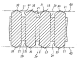
図5は、図4の絶縁性基板2の作製途中の形状を示す縦断面図(基板開口部4の周方向に沿った断面図)である。まず、熱膨張の小さいエンジニアリングプラスチックを、圧縮成形法あるいは注形法等のモールド法により図5に示すような断面形状の板に成形する。即ち、平面23の幅W1よりもさらに小さな幅の頂部33を有する複数の仕切部21と複数の溝部20とをエンジニアリングプラスチックの板の表面及び裏面に交互に形成する。
【0026】
その後、表面及び裏面の溝部20の端部間にエンジニアリングプラスチックの板を貫通する複数の貫通孔を形成した後、この板全面及び貫通孔の内面に乾式めっきあるいは湿式めっきによって導電膜を付着させる。これにより、均一な厚さで導電膜を板全面及び貫通孔の内面に付着させることができる。
それから、エンジニアリングプラスチックの板の表面、裏面、外側面及び基板開口部4の内側面にポリッシングを行い、溝部20の内面及び貫通孔の内面を除く導電膜を除去する。このとき、エンジニアリングプラスチックの板の表面及び裏面では、仕切部21の頂部33が導電膜とともにポリッシング位置40まで除去される。これにより、導電膜が溝部20ごとに分離されて各導体部となる。コイル本体3は、溝部20の内面及び貫通孔の内面に残された導電膜により構成され、空芯コイル1が完成する。
【0027】
このように頂部33の幅が平面23の幅W1よりも小さくなっているので、導電膜をポリッシングにより容易に除去することができる。また、仕切部21に形成された平面23の幅W1が基部24の幅W2よりも小さくなっているので、除去される導電膜の量を少なくでき、導電膜を短時間で除去することができる。従って、大量に、しかも安価に空芯コイル1を製造することができる。
【0028】
また、第2内側接続導体部18は、第1内側接続導体部13よりも基板開口部4に近い側に配置され、第2外側接続導体部19は、第1外側接続導体部14よりも基板開口部4に近い側、かつ第1内側接続導体部13よりも基板開口部4から遠い側に配置されているので、基板開口部4の周方向に沿って見たときに、コイル本体3での巻き進みコイル部5及び巻き戻しコイル部6のそれぞれの断面領域の大部分が互いに重なった状態で、各断面領域の面積をほぼ同一とすることができる。このことから、巻き進みコイル部5及び巻き戻しコイル部6に誘導起電力を発生させる磁束をさらに共通化することができ、また各コイルに発生する誘導起電力の大きさをほぼ等しくすることができる。従って、電流センサに空芯コイル1を用いると、測定感度を向上させることができ、また測定誤差も小さくすることができる。
【0029】
また、コイル本体3の導線は、ほとんど完全に基板開口部4の軸線に関して対称に、かつ均一に形成されることが可能であるので、さらに測定感度を向上させ、測定誤差を小さくすることができる。
【0030】
また、絶縁性基板2は、モールド法により成形されているので、絶縁性基板2の寸法及び形状に制限がなく、コイル本体3の形状も容易に所望の形状にすることができる。
【0031】
実施の形態2.
図6は、この発明の実施の形態2による空芯コイルの構成を示す正面図である。また、図7は、図6の接続点7付近のコイル本体3を示す部分拡大図である。図において、図1の空芯コイル1に相当する部材あるいは部位については同一符号を付して示し、ここでは、その説明を省略する。
【0032】
この実施の形態2による空芯コイル1のコイル本体3は、絶縁性基板2に設けられて互いに直列に接続された巻き進みコイル部5及び巻き戻しコイル部6を有している。
【0033】
図6に示すように、絶縁性基板2の厚さ方向に沿って見たとき、巻き進みコイル部5の各第1表面導体部10及び各第1裏面導体部11により鋸歯状の模様が構成されている。また、巻き戻しコイル部6の各第2表面導体部15及び各第2裏面導体部16によっても鋸歯状の模様が構成され、巻き戻しコイル部6の鋸歯状の模様は、巻き進みコイル部5の鋸歯状の模様の内側に配置されている。巻き進みコイル部5及び巻き戻しコイル部6の導線によってそれぞれ囲まれる鋸歯状の領域は、巻き進みコイル部5の正面領域及び巻き戻しコイル部6の正面領域である。
【0034】
即ち、絶縁性基板2の厚さ方向に沿って視たとき、第2外側接続導体部19を介して互いに接続された第2表面導体部15及び第2裏面導体部16の各内側端部15a、16aは、各第2表面導体部15及び各第2裏面導体部16の配列方向に沿って互いに離間されて配置されている。さらに、第2内側接続導体部18を介して互いに接続された第2表面導体部15及び第2裏面導体部16の各外側端部15b、16bも、各第2表面導体部15及び各第2裏面導体部16の配列方向に沿って互いに離間されて配置されている。
【0035】
また、絶縁性基板2の厚さ方向に沿って視たとき、第1外側接続導体部14を介して互いに接続された第1表面導体部10及び第1裏面導体部11の各内側端部10a、11aは、各第1表面導体部10及び各第1裏面導体部11の配列方向に沿って互いに離間されて配置されている。さらに、第1内側接続導体部13を介して互いに接続された第1表面導体部10及び第1裏面導体部11の各外側端部10b、11bも、各第1表面導体部10及び各第1裏面導体部11の配列方向に沿って互いに離間されて配置されている。
【0036】
さらに、各第2表面導体部15及び各第2裏面導体部16の内側端部15a及び16aは、各第1表面導体部10及び各第1裏面導体部11の内側端部10a及び11aよりも基板開口部4に近い側に配置されている。また、各第2表面導体部15及び各第2裏面導体部16の外側端部15b及び16bは、各第1表面導体部10及び各第1裏面導体部11の外側端部10b及び11bよりも基板開口部4に近い側に配置され、かつ各第1表面導体部10及び各第1裏面導体部11の内側端部10a及び11aよりも基板開口部4から遠い側に配置されている。
【0037】
第1表面導体部10及び第1裏面導体部11が、互いに重なっている外側端部10b及び外側端部11bを始点としたベクトルであると考えると、そのベクトルの合成方向に基板開口部4の中心点が存在するように、各第1表面導体部10及び各第1裏面導体部11は設けられている。
第2表面導体部15及び第2裏面導体部16も同様に、互いに重なっている外側端部15b及び外側端部16bを始点としたベクトルであると考えると、そのベクトルの合成方向に基板開口部4の中心点が存在するように、各第2表面導体部15及び各第2裏面導体部16は設けられている。
他の構成、作製方法及び動作は実施の形態1と同様である。
【0038】
ここで、巻き進みコイル部5及び巻き戻しコイル部6での誘導電流は、被測定導体からの磁界だけでなく、巻き進みコイル部5及び巻き戻しコイル部6のそれぞれの正面領域を通る外部電磁界によっても発生する。外部電磁界による誘導電流は、電流センサの測定誤差の原因となる。従って、外部電磁界による誘導電流を互いに相殺させるために、巻き進みコイル部5及び巻き戻しコイル部6のそれぞれの正面領域の面積が同一に近いほうがよい。
【0039】
従って、実施の形態2による空芯コイル1によれば、実施の形態1と同様の効果を奏するとともに、巻き進みコイル部5の正面領域の面積と巻き戻しコイル部31の正面領域の面積との面積差をさらに小さくすることができ、外部電磁界による測定誤差をさらに小さくすることができる。
【0040】
なお、上記実施の形態1及び2では、ポリッシングにより導電膜を除去しているが、例えば、導電膜を除去したい部分にレジスト剤を塗布しておき、絶縁性基板2の全面に導電膜を付着させた後にレジスト剤と共に導電膜を除去してもよいし、あるいはレーザー等により除去したい導電膜をカットしてもよい。
【0041】
また、上記実施の形態1及び2では、絶縁性基板2は、モールド法による成形に限定されず、例えば切削により成形しても構わない。
【0042】
また、上記実施の形態1及び2では、電流センサの測定感度をさらに向上させるために、複数枚の空芯コイル1を接続して用いてもよい。この場合、信号処理回路32は、複数枚の空芯コイル1に対して1つ設けられる。各空芯コイル1は、基板開口部4を揃えて並べられ、各コイル本体3を互いに接続するために、表面8及び裏面9の一方に引出部30からの接続端子が設けられ、他方に引出部31からの接続端子が設けられる。また、各接続端子同士の接続を容易にするために、互いの接続端子に凹部及び凸部がそれぞれ形成され、この凹部及び凸部が嵌め合わされることにより各接続端子は互いに接続される。
【0043】
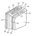
また、上記実施の形態1及び2では、各第2内側接続導体部18及び各第1外側接続導体部14は、貫通孔の内面に付着された導電膜であるが、実施の形態1の変形例を示す図8のように、基板開口部4の内側面及び絶縁性基板2の外側面にそれぞれ形成された複数の内側溝部34及び外側溝部35の内面に付着された導電膜であってもよい。これにより、絶縁性基板2に形成される貫通孔の数を少なくすることができ、さらに容易に各第2内側接続導体部18及び各第1外側接続導体部14を構成することができる。この場合、各内側溝部34間及び各外側溝部35間の仕切部36の先端部(各溝部34及び35の解放側)には、テーパ面37が形成される。
また、貫通孔、内側溝部34及び外側溝部35を混在させて各第2内側接続導体部18及び各第1外側接続導体部14を構成しても構わない。
【0044】
実施の形態3.
図9は、この発明の実施の形態3による空芯コイルの構成を示す部分斜視図である。図において、実施の形態1又は2での絶縁性基板2の外側面及び基板開口部4の内側面には、導電膜である導電性シールド41が付着されている。導電性シールド41は、例えば銅等の導電性金属が電気的に接地されたものである。
【0045】
導電性シールド41は、上記実施の形態1での空芯コイル1の作製途中において、絶縁性基板2の全面に導電膜を付着させた後のポリッシングの際、絶縁性基板2の外側面及び基板開口部4の内側面のポリッシングを行わずに導電膜を残すことにより形成される。
【0046】
ここで、絶縁性基板2に設けられたコイル本体3(図1参照)の接続導体部12及び17(図2参照)は、貫通孔の内面に付着された導電膜であり、導電性シールド41に対して短絡しないようになっている。他の構成は実施の形態1と同様である。
【0047】
このように絶縁性基板2の外側面及び基板開口部4の内側面に導電性シールド41が付着されているので、コイル本体3(図1参照)での外部電磁界による誘導起電力の発生を導電性シールド41によって抑制することができる。ここで、導電性シールド41は、接地されているので、外部電磁界により発生した誘導起電力によって帯電することはない。
【0048】
実施の形態4.
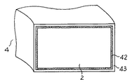
図10は、この発明の実施の形態3による空芯コイルの構成を示す部分斜視図である。図において、実施の形態1あるいは2での絶縁性基板2の表面、裏面、外側面及び基板開口部4の内側面には、絶縁性材料の絶縁層42が設けられている。絶縁層42の外周面には、導電膜である導電性シールド43が付着されている。即ち、コイル本体3(図1参照)及び絶縁性基板2は、絶縁層42を介して導電性シールド43に覆われている(即ち、囲まれている)。導電性シールド43は、例えば銅等の導電性金属が電気的に接地されたものである。他の構成は実施の形態1と同様である。
【0049】
このようにコイル本体3(図1参照)が導電性シールド43によって囲まれているので、コイル本体3(図1参照)での外部電磁界による誘導起電力の発生を導電性シールド41によってさらに抑制することができる。
【0050】
なお、絶縁層42は、絶縁性基板2を完全に囲う必要はなく、導電性シールド43が内部のコイル本体3(図1参照)に接触しない状態に保たれていれば、例えば格子状、あるいは複数の支持突起であってもよい。
【0051】
また、実施の形態3及び4では、導電性シールド41及び43は導電膜であるが、例えば金属板であってもよい。
また、実施の形態1による空芯コイルに代えて、実施の形態2による空芯コイルを用いると、電流センサの外部電磁界による測定誤差をさらに小さくすることができる。
【0052】
【発明の効果】
以上の説明から明らかなように、この発明に係る空芯コイルは、表面及び裏面の少なくとも一方には、基板開口部の周囲で略放射状に延びる複数の溝部と複数の仕切部とが交互に配列され、導体部が各溝部にそれぞれ設けられており、仕切部の先端部の幅は、仕切部の基部の幅よりも小さくなっているので、表面あるいは裏面に導電膜を付着させて溝部内に導電膜を導体部として残す方法で、除去される導電膜の量を少なくでき、導体部を短時間で形成することができる。
【図面の簡単な説明】
【図1】図1は、この発明の実施の形態1による空芯コイルを示す正面図である。
【図2】図1の接続点付近のコイル本体を示す部分拡大図である。
【図3】図1の基板開口部の外周に沿って見たときの絶縁性基板、巻き進みコイル部及び巻き戻しコイル部を示す配置図である。
【図4】図3のIV−IV線に沿った断面図である。
【図5】図4の絶縁性基板の作製途中の形状を示す基板開口部の周方向に沿った断面図である。
【図6】この発明の実施の形態2による空芯コイルの構成を示す正面図である。
【図7】図6の接続点付近のコイル本体を示す部分拡大図である。
【図8】この発明の実施の形態1の変形例による空芯コイルを示す部分斜視図である。
【図9】この発明の実施の形態3による空芯コイルの構成を示す部分斜視図である。
【図10】この発明の実施の形態4による空芯コイルの構成を示す部分斜視図である。
【符号の説明】
1 空芯コイル、2 絶縁性基板、3 コイル本体、4 基板開口部、5 巻き進みコイル部、6 巻き戻しコイル部、8 表面、9 裏面、10 第1表面導体部(表面導体部)、11 第1裏面導体部(裏面導体部)、12,17 接続導体部、13 第1内側接続導体部(内側接続導体部)、14 第1外側接続導体部(外側接続導体部)、15 第2表面導体部(表面導体部)、16 第2裏面導体部(裏面導体部)、18 第2内側接続導体部(内側接続導体部)、19 第2外側接続導体部(外側接続導体部)、20 溝部、21,36 仕切部、22 先端部、24 基部、33 頂部、34 内側溝部、35 外側溝部。[0001]
TECHNICAL FIELD OF THE INVENTION
The present invention relates to an air-core coil used for a current sensor for measuring, for example, a large impulse current flowing through a conductor to be measured.
[0002]
[Prior art]
An air-core coil is a coil that does not have a ferromagnetic material such as an iron core in a winding core, and has a property of not causing magnetic saturation. Therefore, when the air-core coil is used as a current sensor for measuring the current flowing through the conductor to be measured, a wide current range can be measured. A Rogowski coil is used for the air-core coil of the current sensor in order to suppress a measurement error due to an external electromagnetic field. The Rogowski coil is a coil in which a conductive wire is wound in a solenoid shape and returned from the end to the beginning of winding.
[0003]
Conventional Rogowski coils are constructed by depositing gold on a planar printed circuit board. Since this Rogowski coil is formed on a flat printed circuit board, it can be manufactured almost completely symmetrically in the axial direction (for example, see Patent Document 1).
[0004]
[Patent Document 1]
JP-A-6-176947
[0005]
[Problems to be solved by the invention]
As described above, when manufacturing the conventional air-core coil, it is necessary to arrange the gold deposit on the planar printed circuit board in a pattern, which is troublesome.
In addition, when a conventional air-core coil is used for a current sensor, when viewed along the axis of the conductor to be measured, the area surrounded by the leading coil of the Rogowski coil differs from the area surrounded by the rewind coil. Therefore, a difference occurs in the magnitude of the induced electromotive force generated in each case, and the measurement error increases.
[0006]
Therefore, an object of the present invention is to solve the above-described problems, and an object of the present invention is to obtain an air-core coil that has a small measurement error and is easy to manufacture.
[0007]
[Means for Solving the Problems]
An air-core coil according to the present invention is an insulating substrate having a front surface, a back surface, and a substrate opening that penetrates the front and back surfaces and through which a conductor to be measured is passed, around the substrate opening on the front and back surfaces. A plurality of conductors provided in a substantially radial manner, and a plurality of connection conductors connected to respective ends of the conductors on the front surface and the conductors on the back surface; A plurality of grooves and a plurality of partitions extending substantially radially around the substrate opening are alternately arranged on at least one of the front surface and the back surface, and the conductor portion is provided on at least one of the front surface and the back surface. The width of the tip of the partition is smaller than the width of the base of the partition.
[0008]
BEST MODE FOR CARRYING OUT THE INVENTION
Hereinafter, embodiments of the present invention will be described with reference to the drawings.
Embodiment 1 FIG.
FIG. 1 is a front view showing an air-core coil according to Embodiment 1 of the present invention, and FIG. 2 is a partially enlarged view showing a coil main body 3 near a
[0009]
The
That is, the air-core coil 1 includes a
[0010]
A
[0011]
A plurality of first surface conductors 10 (conductors), which are conductive films, and a plurality of first back surface conductors 11 (conductors), which are conductive films, are respectively attached to the
[0012]
On the
[0013]
Each of the
[0014]
Each of the
[0015]
The
[0016]
Each second
[0017]
As shown in FIG. 1, the substantially radial portions of each of the first
When viewed along the thickness direction of the insulating
[0018]
The connecting
[0019]
The connecting
[0020]
FIG. 3 shows the insulating
The
[0021]
Further, the second
[0022]
That is, the winding
[0023]
FIG. 4 is a sectional view taken along the line IV-IV in FIG. In the figure, a
[0024]
Next, the operation will be described.
When a current flows through the conductor to be measured, a magnetic flux passes through a cross-sectional area of the winding
[0025]
Next, a manufacturing method will be described.
FIG. 5 is a vertical cross-sectional view (cross-sectional view along the circumferential direction of the substrate opening 4) showing the shape of the insulating
[0026]
Then, after forming a plurality of through holes penetrating the engineering plastic plate between the ends of the
Then, polishing is performed on the front surface, the back surface, the outer surface, and the inner surface of the
[0027]
Since the width of the top 33 is smaller than the width W1 of the
[0028]
Further, the second
[0029]
Further, since the conducting wire of the coil body 3 can be formed almost completely symmetrically and uniformly with respect to the axis of the
[0030]
In addition, since the insulating
[0031]
FIG. 6 is a front view showing the configuration of the air-core coil according to
[0032]
The coil body 3 of the air-core coil 1 according to the second embodiment has a winding
[0033]
As shown in FIG. 6, when viewed along the thickness direction of the insulating
[0034]
That is, when viewed along the thickness direction of the insulating
[0035]
Further, when viewed along the thickness direction of the insulating
[0036]
Furthermore, the inner ends 15a and 16a of each of the second
[0037]
Assuming that the first front
Similarly, assuming that the second front
Other configurations, manufacturing methods, and operations are the same as those in the first embodiment.
[0038]
Here, the induced current in the winding
[0039]
Therefore, according to the air-core coil 1 according to the second embodiment, the same effect as that of the first embodiment can be obtained, and the area of the front area of the winding
[0040]
In the first and second embodiments, the conductive film is removed by polishing. For example, a resist agent is applied to a portion where the conductive film is to be removed, and the conductive film is adhered to the entire surface of the insulating
[0041]
In the first and second embodiments, the insulating
[0042]
In
[0043]
In the first and second embodiments, each of the second
Further, the second
[0044]
Embodiment 3 FIG.
FIG. 9 is a partial perspective view showing a configuration of an air-core coil according to Embodiment 3 of the present invention. In the figure, a
[0045]
The
[0046]
Here, the
[0047]
As described above, since the
[0048]
FIG. 10 is a partial perspective view showing a configuration of an air-core coil according to Embodiment 3 of the present invention. In the figure, an insulating
[0049]
Since the coil main body 3 (see FIG. 1) is thus surrounded by the
[0050]
Note that the insulating
[0051]
In the third and fourth embodiments, the
When the air-core coil according to the second embodiment is used instead of the air-core coil according to the first embodiment, the measurement error due to the external electromagnetic field of the current sensor can be further reduced.
[0052]
【The invention's effect】
As is apparent from the above description, in the air-core coil according to the present invention, on at least one of the front surface and the rear surface, a plurality of grooves and a plurality of partitions extending substantially radially around the substrate opening are alternately arranged. The conductor portion is provided in each groove portion, and the width of the tip portion of the partition portion is smaller than the width of the base portion of the partition portion. With the method in which the conductive film is left as a conductor, the amount of the removed conductive film can be reduced, and the conductor can be formed in a short time.
[Brief description of the drawings]
FIG. 1 is a front view showing an air-core coil according to Embodiment 1 of the present invention.
FIG. 2 is a partially enlarged view showing a coil main body near a connection point in FIG. 1;
FIG. 3 is a layout diagram showing an insulating substrate, a winding coil unit, and a rewind coil unit when viewed along the outer periphery of the substrate opening in FIG. 1;
FIG. 4 is a sectional view taken along the line IV-IV in FIG. 3;
FIG. 5 is a cross-sectional view taken along a circumferential direction of a substrate opening showing a shape of the insulating substrate in FIG. 4 in the process of being manufactured.
FIG. 6 is a front view showing a configuration of an air-core coil according to
FIG. 7 is a partially enlarged view showing a coil main body near a connection point in FIG. 6;
FIG. 8 is a partial perspective view showing an air-core coil according to a modification of the first embodiment of the present invention.
FIG. 9 is a partial perspective view showing a configuration of an air-core coil according to Embodiment 3 of the present invention.
FIG. 10 is a partial perspective view showing a configuration of an air-core coil according to
[Explanation of symbols]
REFERENCE SIGNS LIST 1 air core coil, 2 insulating substrate, 3 coil body, 4 substrate opening, 5 winding advance coil, 6 rewind coil, 8 front, 9 back, 10 first surface conductor (surface conductor), 11 1st back side conductor (back side conductor), 12, 17 connection conductor, 13 1st inside connection conductor (inside connection conductor), 14 1st outside connection conductor (outside connection conductor), 15 2nd surface Conductor (front surface conductor), 16 second back surface conductor (back surface conductor), 18 second inner connection conductor (inner connection conductor), 19 second outer connection conductor (outer connection conductor), 20 groove , 21, 36 partition, 22 tip, 24 base, 33 top, 34 inner groove, 35 outer groove.
Claims (7)
上記表面及び上記裏面での上記基板開口部の周囲で略放射状に設けられた複数の導体部と、上記表面の各上記導体部及び上記裏面の各上記導体部のそれぞれの端部に接続された複数の接続導体部とを有し、各上記導体部及び各上記接続導体部によりコイル状に構成されたコイル本体
を備え、
上記表面及び上記裏面の少なくとも一方には、上記基板開口部の周囲で略放射状に延びる複数の溝部と複数の仕切部とが交互に配列され、上記導体部が各上記溝部にそれぞれ設けられており、
上記仕切部の先端部の幅は、上記仕切部の基部の幅よりも小さくなっていることを特徴とする空芯コイル。An insulating substrate having a front surface, a back surface, and a substrate opening penetrating the front surface and the back surface and through which a conductor to be measured is passed;
A plurality of conductor portions provided substantially radially around the substrate opening on the front surface and the back surface, and connected to respective ends of the conductor portions on the front surface and the conductor portions on the back surface. A plurality of connection conductors, comprising a coil body configured in a coil shape by each of the conductors and each of the connection conductors,
On at least one of the front surface and the back surface, a plurality of grooves and a plurality of partitions extending substantially radially around the substrate opening are alternately arranged, and the conductor is provided in each of the grooves. ,
An air-core coil, wherein the width of the leading end of the partition is smaller than the width of the base of the partition.
上記基板開口部の周囲で導線が巻回されて構成され、上記基板開口部を囲むように上記絶縁性基板に設けられた巻き進みコイル部、及び上記基板開口部の周囲で導線が巻回されて構成され、上記巻き進みコイル部とともに上記基板開口部を囲むように上記絶縁性基板に設けられた巻き戻しコイル部を有し、上記被測定導体を流れる電流により上記巻き進みコイル部及び上記巻き戻しコイル部に発生する誘導起電力が電気的に同じ向きになるように上記巻き進みコイル部及び上記巻き戻しコイル部が直列に接続されて構成されたコイル本体と
を備え、
上記絶縁性基板は、上記表面及び上記裏面にそれぞれ設けられて上記基板開口部の周囲で略放射状に形成された複数の溝部を有し、
上記巻き進みコイル部及び上記巻き戻しコイル部は、上記表面の各上記溝部に形成されて上記基板開口部に近い側の内側端部と遠い側の外側端部とを有する複数の表面導体部、上記裏面の各上記溝部に形成されて上記基板開口部の近い側の内側端部と遠い側の外側端部とを有する複数の裏面導体部、互いに隣接する上記裏面導体部のうちの一方の上記裏面導体部の内側端部と上記表面導体部の内側端部とを電気的に接続する複数の内側接続導体部、及び他方の上記裏面導体部の外側端部とその表面導体部の外側端部とを電気的に接続する複数の外側接続導体部をそれぞれ有しており、
上記絶縁性基板の厚さ方向に沿って見たときに、上記巻き進みコイル部及び上記巻き戻しコイル部のうちの一方は、各上記内側接続導体部が他方の各上記内側接続導体部よりも上記基板開口部に近い側に配置され、各上記外側接続導体部が上記他方の各外側接続導体部よりも上記基板開口部に近い側、かつ上記他方の内側接続導体部よりも上記基板開口部から遠い側に配置されていることを特徴とする空芯コイル。A front surface, a back surface, and an insulating substrate having a substrate opening that penetrates the front surface and the back surface and through which the conductor to be measured is passed;
A conductor is wound around the substrate opening, a winding coil provided on the insulating substrate so as to surround the substrate opening, and a conductor is wound around the substrate opening. A winding coil portion provided on the insulating substrate so as to surround the substrate opening together with the winding coil portion, wherein the winding coil portion and the winding coil are driven by a current flowing through the conductor to be measured. A coil main body formed by connecting the winding coil section and the rewind coil section in series so that the induced electromotive force generated in the return coil section is electrically in the same direction,
The insulating substrate has a plurality of grooves provided on the front surface and the rear surface, respectively, and formed substantially radially around the substrate opening,
A plurality of surface conductor portions, wherein the winding advance coil portion and the rewind coil portion are formed in the grooves on the surface and have an inner end closer to the substrate opening and an outer end farther from the substrate opening; A plurality of back surface conductors formed in each of the grooves on the back surface and having an inner end on the near side and an outer end on the far side of the substrate opening, and one of the back surface conductors adjacent to each other; A plurality of inner connection conductors for electrically connecting an inner end of the back conductor and an inner end of the front conductor, and an outer end of the other back conductor and an outer end of the front conductor; Each having a plurality of outer connection conductors electrically connecting the
When viewed along the thickness direction of the insulating substrate, one of the winding coil portion and the rewind coil portion is such that each of the inner connection conductors is greater than the other of the inner connection conductors. The outer connection conductors are arranged closer to the substrate opening, and the outer connection conductors are closer to the substrate opening than the other outer connection conductors, and the substrate opening is closer to the other inner connection conductor. An air-core coil, which is disposed on a side far from the air-core coil.
上記基板開口部に近い側の各上記内側接続導体部のうち、少なくとも1つは、上記内側溝部に設けられていることを特徴とする請求項3に記載の空芯コイル。The insulating substrate has a plurality of inner grooves formed on the inner surface of the substrate opening and extending from the front surface to the rear surface,
The air-core coil according to claim 3, wherein at least one of the inner connection conductors on the side closer to the substrate opening is provided in the inner groove.
上記基板開口部から遠い側の各上記外側接続導体部のうち、少なくとも1つは、上記外側溝部に設けられていることを特徴とする請求項3又は請求項4に記載の空芯コイル。A plurality of outer grooves provided on the outer surface and extending from the front surface to the back surface are formed on the insulating substrate,
5. The air-core coil according to claim 3, wherein at least one of the outer connection conductors farther from the substrate opening is provided in the outer groove.
Priority Applications (1)
| Application Number | Priority Date | Filing Date | Title |
|---|---|---|---|
| JP2003013517A JP2004228296A (en) | 2003-01-22 | 2003-01-22 | Air core coil |
Applications Claiming Priority (1)
| Application Number | Priority Date | Filing Date | Title |
|---|---|---|---|
| JP2003013517A JP2004228296A (en) | 2003-01-22 | 2003-01-22 | Air core coil |
Publications (1)
| Publication Number | Publication Date |
|---|---|
| JP2004228296A true JP2004228296A (en) | 2004-08-12 |
Family
ID=32901824
Family Applications (1)
| Application Number | Title | Priority Date | Filing Date |
|---|---|---|---|
| JP2003013517A Pending JP2004228296A (en) | 2003-01-22 | 2003-01-22 | Air core coil |
Country Status (1)
| Country | Link |
|---|---|
| JP (1) | JP2004228296A (en) |
Cited By (4)
| Publication number | Priority date | Publication date | Assignee | Title |
|---|---|---|---|---|
| US7227441B2 (en) * | 2005-02-04 | 2007-06-05 | Schweitzer Engineering Laboratories, Inc. | Precision Rogowski coil and method for manufacturing same |
| US7545138B2 (en) | 2006-07-06 | 2009-06-09 | Schweitzer Engineering Laboratories, Inc. | Precision, temperature-compensated, shielded current measurement device |
| US8928337B2 (en) | 2012-01-27 | 2015-01-06 | Schweitzer Engineering Laboratories, Inc. | Device for measuring electrical current and method of manufacturing the same |
| US12504446B2 (en) | 2023-12-19 | 2025-12-23 | Schweitzer Engineering Laboratories, Inc. | Fault current sensor with adjacent phase fault immunity |
-
2003
- 2003-01-22 JP JP2003013517A patent/JP2004228296A/en active Pending
Cited By (6)
| Publication number | Priority date | Publication date | Assignee | Title |
|---|---|---|---|---|
| US7227441B2 (en) * | 2005-02-04 | 2007-06-05 | Schweitzer Engineering Laboratories, Inc. | Precision Rogowski coil and method for manufacturing same |
| US7474192B2 (en) * | 2005-02-04 | 2009-01-06 | Schweitzer Engineering Laboratories, Inc. | Precision Rogowski coil and method for manufacturing same |
| US7545138B2 (en) | 2006-07-06 | 2009-06-09 | Schweitzer Engineering Laboratories, Inc. | Precision, temperature-compensated, shielded current measurement device |
| US8928337B2 (en) | 2012-01-27 | 2015-01-06 | Schweitzer Engineering Laboratories, Inc. | Device for measuring electrical current and method of manufacturing the same |
| US12504446B2 (en) | 2023-12-19 | 2025-12-23 | Schweitzer Engineering Laboratories, Inc. | Fault current sensor with adjacent phase fault immunity |
| US12601763B2 (en) | 2023-12-19 | 2026-04-14 | Schweitzer Engineering Laboratories, Inc. | Current sensor with adjacent conductor rejection |
Similar Documents
| Publication | Publication Date | Title |
|---|---|---|
| JP6541677B2 (en) | Antenna and antenna manufacturing method | |
| CN1913724B (en) | Electroacoustic transducer | |
| CN103080752B (en) | Toroidal Fluxgate Current Transducer | |
| CN101897081A (en) | Magnetic antenna and antenna device | |
| US11948735B2 (en) | Method for producing a planar coil assembly and a sensor head provided with same | |
| JP5827840B2 (en) | VR type resolver | |
| JP2000249725A (en) | Manufacture of current sensor | |
| JPWO2003071299A1 (en) | Magnet impedance sensor element with electromagnetic coil | |
| JP4220727B2 (en) | Air core coil | |
| JP2004193215A (en) | Electronic component and method of manufacturing the same | |
| JP2001102230A (en) | Rogowski coil | |
| JP2004087619A (en) | Air core coil | |
| JP4719401B2 (en) | Inductance element | |
| US20020101683A1 (en) | Thin film coil and method of forming the same, thin film magnetic head, thin film inductor and thin film magnetic sensor | |
| EP0497403B1 (en) | Magnetic head and method of manufacturing such a magnetic head | |
| JP2005175156A (en) | Air-core coil and air-core coil manufacturing method | |
| US9607748B2 (en) | Micro-fabricated integrated coil and magnetic circuit and method of manufacturing thereof | |
| KR101018554B1 (en) | Spiral coil manufacturing method and helical coil and electromagnetic acoustic transducer having same | |
| JPH0933488A (en) | Eddy current flaw detection probe and manufacturing method thereof | |
| JP2007201203A (en) | Reactor | |
| CN109616279B (en) | Inductance element and filter | |
| JP2985079B2 (en) | Magnetic sensor | |
| JP3947028B2 (en) | Air core coil | |
| JP2013182927A (en) | Coil component | |
| JPH04344311A (en) | Thin film magnetic circuit substrate and magnetic head using the same |
Legal Events
| Date | Code | Title | Description |
|---|---|---|---|
| A621 | Written request for application examination |
Free format text: JAPANESE INTERMEDIATE CODE: A621 Effective date: 20041213 |
|
| A977 | Report on retrieval |
Effective date: 20070522 Free format text: JAPANESE INTERMEDIATE CODE: A971007 |
|
| A131 | Notification of reasons for refusal |
Free format text: JAPANESE INTERMEDIATE CODE: A131 Effective date: 20070529 |
|
| A02 | Decision of refusal |
Effective date: 20071002 Free format text: JAPANESE INTERMEDIATE CODE: A02 |