JP2004228582A - 半導体素子の製造方法 - Google Patents
半導体素子の製造方法 Download PDFInfo
- Publication number
- JP2004228582A JP2004228582A JP2004012768A JP2004012768A JP2004228582A JP 2004228582 A JP2004228582 A JP 2004228582A JP 2004012768 A JP2004012768 A JP 2004012768A JP 2004012768 A JP2004012768 A JP 2004012768A JP 2004228582 A JP2004228582 A JP 2004228582A
- Authority
- JP
- Japan
- Prior art keywords
- layer
- semiconductor
- metal
- mask
- mask layer
- Prior art date
- Legal status (The legal status is an assumption and is not a legal conclusion. Google has not performed a legal analysis and makes no representation as to the accuracy of the status listed.)
- Pending
Links
Images




Classifications
-
- H—ELECTRICITY
- H10—SEMICONDUCTOR DEVICES; ELECTRIC SOLID-STATE DEVICES NOT OTHERWISE PROVIDED FOR
- H10P—GENERIC PROCESSES OR APPARATUS FOR THE MANUFACTURE OR TREATMENT OF DEVICES COVERED BY CLASS H10
- H10P14/00—Formation of materials, e.g. in the shape of layers or pillars
- H10P14/20—Formation of materials, e.g. in the shape of layers or pillars of semiconductor materials
- H10P14/32—Formation of materials, e.g. in the shape of layers or pillars of semiconductor materials characterised by intermediate layers between substrates and deposited layers
- H10P14/3202—Materials thereof
- H10P14/3214—Materials thereof being Group IIIA-VA semiconductors
- H10P14/3216—Nitrides
-
- B—PERFORMING OPERATIONS; TRANSPORTING
- B82—NANOTECHNOLOGY
- B82Y—SPECIFIC USES OR APPLICATIONS OF NANOSTRUCTURES; MEASUREMENT OR ANALYSIS OF NANOSTRUCTURES; MANUFACTURE OR TREATMENT OF NANOSTRUCTURES
- B82Y20/00—Nanooptics, e.g. quantum optics or photonic crystals
-
- H—ELECTRICITY
- H10—SEMICONDUCTOR DEVICES; ELECTRIC SOLID-STATE DEVICES NOT OTHERWISE PROVIDED FOR
- H10H—INORGANIC LIGHT-EMITTING SEMICONDUCTOR DEVICES HAVING POTENTIAL BARRIERS
- H10H20/00—Individual inorganic light-emitting semiconductor devices having potential barriers, e.g. light-emitting diodes [LED]
- H10H20/01—Manufacture or treatment
- H10H20/011—Manufacture or treatment of bodies, e.g. forming semiconductor layers
- H10H20/013—Manufacture or treatment of bodies, e.g. forming semiconductor layers having light-emitting regions comprising only Group III-V materials
-
- H—ELECTRICITY
- H10—SEMICONDUCTOR DEVICES; ELECTRIC SOLID-STATE DEVICES NOT OTHERWISE PROVIDED FOR
- H10H—INORGANIC LIGHT-EMITTING SEMICONDUCTOR DEVICES HAVING POTENTIAL BARRIERS
- H10H20/00—Individual inorganic light-emitting semiconductor devices having potential barriers, e.g. light-emitting diodes [LED]
- H10H20/80—Constructional details
- H10H20/81—Bodies
- H10H20/815—Bodies having stress relaxation structures, e.g. buffer layers
-
- H—ELECTRICITY
- H10—SEMICONDUCTOR DEVICES; ELECTRIC SOLID-STATE DEVICES NOT OTHERWISE PROVIDED FOR
- H10H—INORGANIC LIGHT-EMITTING SEMICONDUCTOR DEVICES HAVING POTENTIAL BARRIERS
- H10H20/00—Individual inorganic light-emitting semiconductor devices having potential barriers, e.g. light-emitting diodes [LED]
- H10H20/80—Constructional details
- H10H20/81—Bodies
- H10H20/819—Bodies characterised by their shape, e.g. curved or truncated substrates
-
- H—ELECTRICITY
- H10—SEMICONDUCTOR DEVICES; ELECTRIC SOLID-STATE DEVICES NOT OTHERWISE PROVIDED FOR
- H10P—GENERIC PROCESSES OR APPARATUS FOR THE MANUFACTURE OR TREATMENT OF DEVICES COVERED BY CLASS H10
- H10P14/00—Formation of materials, e.g. in the shape of layers or pillars
- H10P14/20—Formation of materials, e.g. in the shape of layers or pillars of semiconductor materials
- H10P14/24—Formation of materials, e.g. in the shape of layers or pillars of semiconductor materials using chemical vapour deposition [CVD]
-
- H—ELECTRICITY
- H10—SEMICONDUCTOR DEVICES; ELECTRIC SOLID-STATE DEVICES NOT OTHERWISE PROVIDED FOR
- H10P—GENERIC PROCESSES OR APPARATUS FOR THE MANUFACTURE OR TREATMENT OF DEVICES COVERED BY CLASS H10
- H10P14/00—Formation of materials, e.g. in the shape of layers or pillars
- H10P14/20—Formation of materials, e.g. in the shape of layers or pillars of semiconductor materials
- H10P14/29—Formation of materials, e.g. in the shape of layers or pillars of semiconductor materials characterised by the substrates
- H10P14/2901—Materials
- H10P14/2902—Materials being Group IVA materials
- H10P14/2904—Silicon carbide
-
- H—ELECTRICITY
- H10—SEMICONDUCTOR DEVICES; ELECTRIC SOLID-STATE DEVICES NOT OTHERWISE PROVIDED FOR
- H10P—GENERIC PROCESSES OR APPARATUS FOR THE MANUFACTURE OR TREATMENT OF DEVICES COVERED BY CLASS H10
- H10P14/00—Formation of materials, e.g. in the shape of layers or pillars
- H10P14/20—Formation of materials, e.g. in the shape of layers or pillars of semiconductor materials
- H10P14/29—Formation of materials, e.g. in the shape of layers or pillars of semiconductor materials characterised by the substrates
- H10P14/2901—Materials
- H10P14/2902—Materials being Group IVA materials
- H10P14/2905—Silicon, silicon germanium or germanium
-
- H—ELECTRICITY
- H10—SEMICONDUCTOR DEVICES; ELECTRIC SOLID-STATE DEVICES NOT OTHERWISE PROVIDED FOR
- H10P—GENERIC PROCESSES OR APPARATUS FOR THE MANUFACTURE OR TREATMENT OF DEVICES COVERED BY CLASS H10
- H10P14/00—Formation of materials, e.g. in the shape of layers or pillars
- H10P14/20—Formation of materials, e.g. in the shape of layers or pillars of semiconductor materials
- H10P14/29—Formation of materials, e.g. in the shape of layers or pillars of semiconductor materials characterised by the substrates
- H10P14/2901—Materials
- H10P14/2921—Materials being crystalline insulating materials
-
- H—ELECTRICITY
- H10—SEMICONDUCTOR DEVICES; ELECTRIC SOLID-STATE DEVICES NOT OTHERWISE PROVIDED FOR
- H10P—GENERIC PROCESSES OR APPARATUS FOR THE MANUFACTURE OR TREATMENT OF DEVICES COVERED BY CLASS H10
- H10P14/00—Formation of materials, e.g. in the shape of layers or pillars
- H10P14/20—Formation of materials, e.g. in the shape of layers or pillars of semiconductor materials
- H10P14/32—Formation of materials, e.g. in the shape of layers or pillars of semiconductor materials characterised by intermediate layers between substrates and deposited layers
- H10P14/3202—Materials thereof
- H10P14/3204—Materials thereof being Group IVA semiconducting materials
- H10P14/3208—Silicon carbide
-
- H—ELECTRICITY
- H10—SEMICONDUCTOR DEVICES; ELECTRIC SOLID-STATE DEVICES NOT OTHERWISE PROVIDED FOR
- H10P—GENERIC PROCESSES OR APPARATUS FOR THE MANUFACTURE OR TREATMENT OF DEVICES COVERED BY CLASS H10
- H10P14/00—Formation of materials, e.g. in the shape of layers or pillars
- H10P14/20—Formation of materials, e.g. in the shape of layers or pillars of semiconductor materials
- H10P14/32—Formation of materials, e.g. in the shape of layers or pillars of semiconductor materials characterised by intermediate layers between substrates and deposited layers
- H10P14/3202—Materials thereof
- H10P14/3238—Materials thereof being insulating materials
-
- H—ELECTRICITY
- H10—SEMICONDUCTOR DEVICES; ELECTRIC SOLID-STATE DEVICES NOT OTHERWISE PROVIDED FOR
- H10P—GENERIC PROCESSES OR APPARATUS FOR THE MANUFACTURE OR TREATMENT OF DEVICES COVERED BY CLASS H10
- H10P14/00—Formation of materials, e.g. in the shape of layers or pillars
- H10P14/20—Formation of materials, e.g. in the shape of layers or pillars of semiconductor materials
- H10P14/34—Deposited materials, e.g. layers
- H10P14/3402—Deposited materials, e.g. layers characterised by the chemical composition
- H10P14/3414—Deposited materials, e.g. layers characterised by the chemical composition being group IIIA-VIA materials
- H10P14/3416—Nitrides
Landscapes
- Chemical & Material Sciences (AREA)
- Engineering & Computer Science (AREA)
- Nanotechnology (AREA)
- Physics & Mathematics (AREA)
- Life Sciences & Earth Sciences (AREA)
- Biophysics (AREA)
- Optics & Photonics (AREA)
- Crystallography & Structural Chemistry (AREA)
- Led Devices (AREA)
- Recrystallisation Techniques (AREA)
Abstract
【解決手段】基板31上に、第1半導体層33、マスク層35及び金属層39を順次に積層する第1段階と、金属層39を陽極酸化してナノサイズのホール(ナノホール)が多数形成される金属酸化物層に変化させる第2段階と、ナノホールが第1半導体層33の表面まで延びるように金属酸化物層をマスクとして前記マスク層35をエッチングする第3段階と、金属酸化物層を除去する第4段階と、マスク層及び第1半導体層の上面に第2半導体層を蒸着する第5段階と、を含む半導体素子の製造方法である。格子不整合によって発生する欠陥密度を減少させ、欠陥分布を分散させることができる。
【選択図】図3A
Description
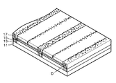
図1及び図2を参照して説明すると、基板11上に第1GaN層13が積層し、その上部に第1GaN層13の一部面積を遮蔽して欠陥Dの垂直方向の成長を阻止させるマスク層15がストライプパターンに形成し、さらに第1GaN層13及びマスク層15の上部に第2GaN層17が再成長する。
前記マスク層は、50nm〜500nmの厚さに形成することが望ましい。
前記第1半導体層及び前記基板は互いに格子定数が相異することが望ましい。
前記第1半導体層及び第2半導体層は、窒化物半導体で形成するが、前記窒化物半導体は、GaN、InGaN、AlGaN、AlInGaN、またはInGaNAsのうち少なくとも一種を含んで形成される。
前記マスク層は、多結晶半導体、誘電物質、または金属で形成できる。ここで、前記多結晶半導体は、多結晶シリコンまたは多結晶窒化物を含み、前記誘電物質は、酸化珪素、酸化チタン、または酸化ジルコニウムを含み、前記金属は、1200℃以上の融点を有するものであって、チタンまたはタングステンで形成することが望ましい。
前記第5段階で、前記マスク層のナノホール内に電荷保存物質をさらに蒸着することが望ましい。
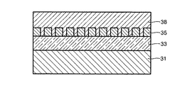
図3A〜図3Eは、欠陥の成長を抑制する本発明の実施例による半導体素子の製造方法を示す工程図である。
ドライエッチング工程の実行後、金属酸化物層39aをエッチングさせて除去すれば、図3Dに示すように第1半導体層33の表面にはナノパターンを有するマスク層35だけが残留する。マスク層35としては、多結晶シリコン、多結晶窒化物半導体のような多結晶半導体、酸化珪素(SiOx)、窒化珪素(SiNx)、酸化チタン(TiOx)、酸化ジルコニウム(ZrOx)のような酸化物・窒化物(誘電物質)またはこのような多層膜以外に1200℃以上の融点を有するチタン(Ti)、タングステン(W)のような高融点金属を利用することができる。
図4に示すように、サファイア基板41上にGaNバッファ層42が積層されており、GaNバッファ層42の上面にはナノホールがストライプまたは六角形に配列されたSiO2層40がパターニングされている。SiO2層40の上面にはn−GaN層43が蒸着され、マスク層であるSiO2層40によってサファイア基板41及びGaNバッファ層42の界面で発生したスレッディングディスロケーションの成長が抑制されて欠陥密度が低下し、ナノホールが均一に分布して欠陥が何れか一部分に集中せずに均一に分布する。n−GaN層43の上面には下部クラッド層としてn−AlGaN層44が、活性層としてInGaN層45が、上部クラッド層としてp−AlGaN層46が順次に積層され、n−GaN層43の段差部分にはn型電極48が形成され、p−AlGaN層46の上面にはp型電極49が形成されている。
図5に示すように、下部クラッド層54の上面にマスク層55をパターニングし、マスク層55のナノホールに電荷保存物質50を充填すれば、量子点を有する発光素子が製造される。ここで、51は基板、52はバッファ層、53は第1半導体層、56は上部クラッド層、57は第2半導体層、58はn型電極、59はp型電極である。
例えば、当業者なら、本発明の技術的思想によって多様な形態のナノパターンを有するマスク層を製造できる。従って、本発明の範囲は、前記実施例によって決定されず、特許請求の範囲に記載された技術的思想によって決定されなければならない。
33 第1半導体層
35 マスク層
39 金属層
Claims (16)
- 基板上に、第1半導体層、マスク層及び金属層を順次に積層する第1段階と、
前記金属層を陽極酸化してナノサイズのホールが多数形成された金属酸化物層を形成する第2段階と、
前記ナノサイズのホールが前記第1半導体層の表面まで延びるように前記金属酸化物層をマスクとして前記マスク層をエッチングする第3段階と、
前記金属酸化物層をエッチングして除去する第4段階と、
前記マスク層及び前記第1半導体層の上面に第2半導体層を蒸着する第5段階と、を含むことを特徴とする半導体素子の製造方法。 - 前記ホールの直径のサイズは、10nm〜500nmであることを特徴とする請求項1に記載の半導体素子の製造方法。
- 前記ホールは、全体面積に対し50%以内の占有面積率で形成されることを特徴とする請求項1に記載の半導体素子の製造方法。
- 前記マスク層は、50nm〜500nmの厚さに形成されることを特徴とする請求項1に記載の半導体素子の製造方法。
- 前記第1半導体層及び前記基板は互いに格子定数が相異することを特徴とする請求項1に記載の半導体素子の製造方法。
- 前記基板は、サファイア、Si、SiC、MgAl2O4、NdGaO3、LiGaO2、ZnO、MgOのうち少なくとも一種を含む無機物結晶、GaP、GaAsのうち少なくとも一種を含む3−5族化合物半導体、またはGaNを少なくとも含む3族窒化物半導体により形成されていることを特徴とする請求項1に記載の半導体素子の製造方法。
- 前記第1半導体層及び第2半導体層は、窒化物半導体であることを特徴とする請求項1に記載の半導体素子の製造方法。
- 前記窒化物半導体は、GaN、InGaN、AlGaN、AlInGaN、またはInGaNAsで表わされる少なくとも一種の化合物から構成されていることを特徴とする請求項7に記載の半導体素子の製造方法。
- 前記マスク層は、多結晶半導体、誘電物質、または金属で形成されていることを特徴とする請求項1に記載の半導体素子の製造方法。
- 前記多結晶半導体は、多結晶シリコンまたは多結晶窒化物から構成されていることを特徴とする請求項9に記載の半導体素子の製造方法。
- 前記誘電物質は、酸化珪素、酸化チタン、または酸化ジルコニウムから構成されていることを特徴とする請求項9に記載の半導体素子の製造方法。
- 前記金属は、1200℃以上の融点を有することを特徴とする請求項9に記載の半導体素子の製造方法。
- 前記金属は、チタンまたはタングステンで構成されていることを特徴とする請求項12に記載の半導体素子の製造方法。
- 前記金属層は、アルミニウムで構成されていることを特徴とする請求項1に記載の半導体素子の製造方法。
- 前記第3段階で、
前記エッチングは、ドライエッチングであることを特徴とする請求項1に記載の半導体素子の製造方法。 - 前記第5段階で、
前記マスク層の前記ホール内に電荷保存物質をさらに蒸着する工程を含むことを特徴とする請求項1に記載の半導体素子の製造方法。
Applications Claiming Priority (1)
| Application Number | Priority Date | Filing Date | Title |
|---|---|---|---|
| KR10-2003-0004106A KR100513316B1 (ko) | 2003-01-21 | 2003-01-21 | 고효율 반도체 소자 제조방법 |
Publications (1)
| Publication Number | Publication Date |
|---|---|
| JP2004228582A true JP2004228582A (ja) | 2004-08-12 |
Family
ID=32709922
Family Applications (1)
| Application Number | Title | Priority Date | Filing Date |
|---|---|---|---|
| JP2004012768A Pending JP2004228582A (ja) | 2003-01-21 | 2004-01-21 | 半導体素子の製造方法 |
Country Status (4)
| Country | Link |
|---|---|
| US (1) | US20040142503A1 (ja) |
| JP (1) | JP2004228582A (ja) |
| KR (1) | KR100513316B1 (ja) |
| CN (1) | CN100379035C (ja) |
Cited By (6)
| Publication number | Priority date | Publication date | Assignee | Title |
|---|---|---|---|---|
| JP2006114802A (ja) * | 2004-10-18 | 2006-04-27 | Toyota Central Res & Dev Lab Inc | Iii−v族半導体層に上部層が積層されている構造体とその製造方法 |
| JP2006165583A (ja) * | 2004-12-08 | 2006-06-22 | Samsung Electro Mech Co Ltd | 高効率半導体発光素子及びその製造方法 |
| JP2007258337A (ja) * | 2006-03-22 | 2007-10-04 | Rohm Co Ltd | 半導体発光素子 |
| JP2009009978A (ja) * | 2007-06-26 | 2009-01-15 | Panasonic Electric Works Co Ltd | 化合物半導体素子およびそれを用いる照明装置ならびに化合物半導体素子の製造方法 |
| CN101863452A (zh) * | 2010-06-10 | 2010-10-20 | 中国科学院苏州纳米技术与纳米仿生研究所 | 一种改善绝缘衬底上纳米阵列结构器件制作的方法 |
| JP2011142294A (ja) * | 2010-01-08 | 2011-07-21 | Taiwan Semiconductor Manufacturing Co Ltd | 光デバイス及びその製造方法 |
Families Citing this family (56)
| Publication number | Priority date | Publication date | Assignee | Title |
|---|---|---|---|---|
| CN100411778C (zh) * | 2004-08-11 | 2008-08-20 | 鸿富锦精密工业(深圳)有限公司 | 纳米金属粉体的制造方法 |
| DE102004041893B4 (de) * | 2004-08-30 | 2006-11-23 | Infineon Technologies Ag | Verfahren zur Herstellung von Speicherbauelementen (PCRAM) mit Speicherzellen auf der Basis einer in ihrem Phasenzustand änderbaren Schicht |
| KR100664986B1 (ko) * | 2004-10-29 | 2007-01-09 | 삼성전기주식회사 | 나노로드를 이용한 질화물계 반도체 소자 및 그 제조 방법 |
| JP4375560B2 (ja) * | 2004-12-07 | 2009-12-02 | セイコーエプソン株式会社 | トランジスタ型強誘電体メモリの製造方法 |
| KR100624449B1 (ko) * | 2004-12-08 | 2006-09-18 | 삼성전기주식회사 | 요철 구조를 포함하는 발광 소자 및 그 제조 방법 |
| US20070145386A1 (en) * | 2004-12-08 | 2007-06-28 | Samsung Electro-Mechanics Co., Ltd. | Semiconductor light emitting device and method of manufacturing the same |
| US9153645B2 (en) | 2005-05-17 | 2015-10-06 | Taiwan Semiconductor Manufacturing Company, Ltd. | Lattice-mismatched semiconductor structures with reduced dislocation defect densities and related methods for device fabrication |
| US8324660B2 (en) | 2005-05-17 | 2012-12-04 | Taiwan Semiconductor Manufacturing Company, Ltd. | Lattice-mismatched semiconductor structures with reduced dislocation defect densities and related methods for device fabrication |
| KR20070081184A (ko) * | 2006-02-10 | 2007-08-16 | 삼성전기주식회사 | 질화물계 반도체 발광소자 및 그 제조방법 |
| US20070224784A1 (en) * | 2006-03-22 | 2007-09-27 | Soloviev Stanislav I | Semiconductor material having an epitaxial layer formed thereon and methods of making same |
| WO2007112066A2 (en) | 2006-03-24 | 2007-10-04 | Amberwave Systems Corporation | Lattice-mismatched semiconductor structures and related methods for device fabrication |
| KR100786091B1 (ko) * | 2006-06-08 | 2007-12-18 | 엘지전자 주식회사 | 수평형 발광 소자 및 그 제조방법 |
| KR100818451B1 (ko) * | 2006-07-03 | 2008-04-01 | 삼성전기주식회사 | 편광성을 갖는 반도체 발광 소자 |
| EP2062290B1 (en) | 2006-09-07 | 2019-08-28 | Taiwan Semiconductor Manufacturing Company, Ltd. | Defect reduction using aspect ratio trapping |
| US7875958B2 (en) | 2006-09-27 | 2011-01-25 | Taiwan Semiconductor Manufacturing Company, Ltd. | Quantum tunneling devices and circuits with lattice-mismatched semiconductor structures |
| WO2008051503A2 (en) * | 2006-10-19 | 2008-05-02 | Amberwave Systems Corporation | Light-emitter-based devices with lattice-mismatched semiconductor structures |
| KR101316120B1 (ko) * | 2006-12-28 | 2013-10-11 | 서울바이오시스 주식회사 | 양극 알루미늄산화를 이용한 산란 중심을 구비하는 발광 소자 제조방법 및 그 발광 소자 |
| WO2008124154A2 (en) | 2007-04-09 | 2008-10-16 | Amberwave Systems Corporation | Photovoltaics on silicon |
| US8237151B2 (en) | 2009-01-09 | 2012-08-07 | Taiwan Semiconductor Manufacturing Company, Ltd. | Diode-based devices and methods for making the same |
| US7825328B2 (en) | 2007-04-09 | 2010-11-02 | Taiwan Semiconductor Manufacturing Company, Ltd. | Nitride-based multi-junction solar cell modules and methods for making the same |
| US8329541B2 (en) | 2007-06-15 | 2012-12-11 | Taiwan Semiconductor Manufacturing Company, Ltd. | InP-based transistor fabrication |
| KR20080114049A (ko) * | 2007-06-26 | 2008-12-31 | 우리엘에스티 주식회사 | 반도체 소자의 제조 방법 |
| JP2010538495A (ja) | 2007-09-07 | 2010-12-09 | アンバーウェーブ・システムズ・コーポレーション | 多接合太陽電池 |
| US8183667B2 (en) | 2008-06-03 | 2012-05-22 | Taiwan Semiconductor Manufacturing Co., Ltd. | Epitaxial growth of crystalline material |
| JP5167974B2 (ja) * | 2008-06-16 | 2013-03-21 | 豊田合成株式会社 | Iii族窒化物系化合物半導体発光素子及びその製造方法 |
| US8274097B2 (en) | 2008-07-01 | 2012-09-25 | Taiwan Semiconductor Manufacturing Company, Ltd. | Reduction of edge effects from aspect ratio trapping |
| US8981427B2 (en) | 2008-07-15 | 2015-03-17 | Taiwan Semiconductor Manufacturing Company, Ltd. | Polishing of small composite semiconductor materials |
| EP2335273A4 (en) | 2008-09-19 | 2012-01-25 | Taiwan Semiconductor Mfg | FORMATION OF EQUIPMENT BY EXCESSIVE GROWTH OF THE EPITAXIAL LAYER |
| US20100072515A1 (en) | 2008-09-19 | 2010-03-25 | Amberwave Systems Corporation | Fabrication and structures of crystalline material |
| US8253211B2 (en) | 2008-09-24 | 2012-08-28 | Taiwan Semiconductor Manufacturing Company, Ltd. | Semiconductor sensor structures with reduced dislocation defect densities |
| TWI470823B (zh) | 2009-02-11 | 2015-01-21 | Epistar Corp | 發光元件及其製造方法 |
| US8629446B2 (en) | 2009-04-02 | 2014-01-14 | Taiwan Semiconductor Manufacturing Company, Ltd. | Devices formed from a non-polar plane of a crystalline material and method of making the same |
| KR100943092B1 (ko) | 2009-05-18 | 2010-02-18 | 주식회사 시스넥스 | 질화물 반도체 발광다이오드 및 이의 제조방법 |
| US8476660B2 (en) * | 2009-08-20 | 2013-07-02 | Integrated Photovoltaics, Inc. | Photovoltaic cell on substrate |
| CN104795314B (zh) * | 2009-08-26 | 2018-02-09 | 首尔伟傲世有限公司 | 制造发光装置的方法 |
| CN102456784B (zh) * | 2010-10-29 | 2014-10-15 | 展晶科技(深圳)有限公司 | 发光二极管及其制造方法 |
| TWI414086B (zh) * | 2010-11-03 | 2013-11-01 | Advanced Optoelectronic Tech | 發光二極體及其製造方法 |
| CN103286910B (zh) | 2012-02-24 | 2015-09-30 | 比亚迪股份有限公司 | 一种金属树脂一体化成型方法和一种金属树脂复合体 |
| CN103286996B (zh) | 2012-02-24 | 2015-03-25 | 比亚迪股份有限公司 | 一种铝合金树脂复合体的制备方法及其制备的铝合金树脂复合体 |
| CN104780241B (zh) | 2012-02-24 | 2018-06-26 | 比亚迪股份有限公司 | 一种手机壳体 |
| CN103286909B (zh) | 2012-02-24 | 2015-09-30 | 比亚迪股份有限公司 | 一种金属树脂一体化成型方法和一种金属树脂复合体 |
| CN103286995B (zh) | 2012-02-24 | 2015-06-24 | 比亚迪股份有限公司 | 一种铝合金树脂复合体的制备方法及其制备的铝合金树脂复合体 |
| CN103286908B (zh) | 2012-02-24 | 2015-09-30 | 比亚迪股份有限公司 | 一种金属树脂一体化成型方法和一种金属树脂复合体 |
| CN103287009B (zh) | 2012-02-24 | 2015-03-25 | 比亚迪股份有限公司 | 一种铝合金树脂复合体的制备方法及其制备的铝合金树脂复合体 |
| WO2013178057A1 (en) * | 2012-05-28 | 2013-12-05 | Shenzhen Byd Auto R&D Company Limited | Metal composite and method of preparing the same, metal-resin composite and method of preparing the same |
| US8772948B2 (en) | 2012-08-30 | 2014-07-08 | Infineon Technologies Ag | Method for manufacturing a layer arrangement, and a layer arrangement |
| KR20150064496A (ko) * | 2013-12-03 | 2015-06-11 | 한국전자통신연구원 | 발광 다이오드 및 그 제조방법 |
| CN104746066B (zh) | 2013-12-31 | 2017-07-04 | 比亚迪股份有限公司 | 一种金属与塑料的结合材料及其制备方法及制备的结合材料 |
| DE102014116999B4 (de) * | 2014-11-20 | 2025-09-18 | OSRAM Opto Semiconductors Gesellschaft mit beschränkter Haftung | Verfahren zur Herstellung eines optoelektronischen Halbleiterchips |
| CN106653968A (zh) * | 2016-12-12 | 2017-05-10 | 上海芯元基半导体科技有限公司 | Iii‑v族氮化物生长用复合衬底、器件结构及制备方法 |
| CN106910675A (zh) * | 2017-03-09 | 2017-06-30 | 东莞市中镓半导体科技有限公司 | 一种用于制备氮化物电子器件的复合衬底及其制备方法 |
| CN108878261B (zh) * | 2018-06-05 | 2021-10-29 | 太原理工大学 | 一种纳米多孔GaN结构及其制备方法 |
| JP6986645B1 (ja) * | 2020-12-29 | 2021-12-22 | 京セラ株式会社 | 半導体基板、半導体デバイス、電子機器 |
| TWI833455B (zh) * | 2022-06-29 | 2024-02-21 | 南亞科技股份有限公司 | 減少陣列區缺陷之半導體元件的製備方法 |
| US12525475B2 (en) | 2022-06-29 | 2026-01-13 | Nanya Technology Corporation | Method of manufacturing semiconductor device using underlayer for reducing defect in array region |
| US12660538B2 (en) | 2022-06-29 | 2026-06-16 | Nanya Technology Corporation | Method of manufacturing semiconductor device for reducing defect in array region |
Citations (8)
| Publication number | Priority date | Publication date | Assignee | Title |
|---|---|---|---|---|
| JPH0878769A (ja) * | 1994-08-31 | 1996-03-22 | Sony Corp | 量子構造の形成方法 |
| JPH11238687A (ja) * | 1998-02-20 | 1999-08-31 | Ricoh Co Ltd | 半導体基板および半導体発光素子 |
| JP2001148348A (ja) * | 1997-03-13 | 2001-05-29 | Nec Corp | GaN系半導体素子とその製造方法 |
| JP2002050585A (ja) * | 2000-08-03 | 2002-02-15 | Hitachi Cable Ltd | 半導体の結晶成長方法 |
| JP2002249400A (ja) * | 2001-02-22 | 2002-09-06 | Mitsubishi Chemicals Corp | 化合物半導体単結晶の製造方法およびその利用 |
| US20030010971A1 (en) * | 2001-06-25 | 2003-01-16 | Zhibo Zhang | Methods of forming nano-scale electronic and optoelectronic devices using non-photolithographically defined nano-channel templates and devices formed thereby |
| JP2003332633A (ja) * | 2002-05-16 | 2003-11-21 | Sony Corp | 表示装置および表示装置の製造方法 |
| JP2004059325A (ja) * | 2001-07-04 | 2004-02-26 | Fuji Photo Film Co Ltd | 半導体素子用基板の製造方法および半導体素子用基板ならびに半導体素子 |
Family Cites Families (6)
| Publication number | Priority date | Publication date | Assignee | Title |
|---|---|---|---|---|
| US534707A (en) * | 1895-02-26 | Combined latch and check | ||
| US5705321A (en) * | 1993-09-30 | 1998-01-06 | The University Of New Mexico | Method for manufacture of quantum sized periodic structures in Si materials |
| US5948470A (en) * | 1997-04-28 | 1999-09-07 | Harrison; Christopher | Method of nanoscale patterning and products made thereby |
| US6596377B1 (en) * | 2000-03-27 | 2003-07-22 | Science & Technology Corporation @ Unm | Thin film product and method of forming |
| CN1123913C (zh) * | 2001-04-20 | 2003-10-08 | 信息产业部电子第十三研究所 | 分子束外延自组织生长量子线的制备方法 |
| US20040077156A1 (en) * | 2002-10-18 | 2004-04-22 | Loucas Tsakalakos | Methods of defect reduction in wide bandgap thin films using nanolithography |
-
2003
- 2003-01-21 KR KR10-2003-0004106A patent/KR100513316B1/ko not_active Expired - Fee Related
- 2003-09-12 US US10/660,561 patent/US20040142503A1/en not_active Abandoned
- 2003-09-17 CN CNB031589480A patent/CN100379035C/zh not_active Expired - Fee Related
-
2004
- 2004-01-21 JP JP2004012768A patent/JP2004228582A/ja active Pending
Patent Citations (8)
| Publication number | Priority date | Publication date | Assignee | Title |
|---|---|---|---|---|
| JPH0878769A (ja) * | 1994-08-31 | 1996-03-22 | Sony Corp | 量子構造の形成方法 |
| JP2001148348A (ja) * | 1997-03-13 | 2001-05-29 | Nec Corp | GaN系半導体素子とその製造方法 |
| JPH11238687A (ja) * | 1998-02-20 | 1999-08-31 | Ricoh Co Ltd | 半導体基板および半導体発光素子 |
| JP2002050585A (ja) * | 2000-08-03 | 2002-02-15 | Hitachi Cable Ltd | 半導体の結晶成長方法 |
| JP2002249400A (ja) * | 2001-02-22 | 2002-09-06 | Mitsubishi Chemicals Corp | 化合物半導体単結晶の製造方法およびその利用 |
| US20030010971A1 (en) * | 2001-06-25 | 2003-01-16 | Zhibo Zhang | Methods of forming nano-scale electronic and optoelectronic devices using non-photolithographically defined nano-channel templates and devices formed thereby |
| JP2004059325A (ja) * | 2001-07-04 | 2004-02-26 | Fuji Photo Film Co Ltd | 半導体素子用基板の製造方法および半導体素子用基板ならびに半導体素子 |
| JP2003332633A (ja) * | 2002-05-16 | 2003-11-21 | Sony Corp | 表示装置および表示装置の製造方法 |
Cited By (9)
| Publication number | Priority date | Publication date | Assignee | Title |
|---|---|---|---|---|
| JP2006114802A (ja) * | 2004-10-18 | 2006-04-27 | Toyota Central Res & Dev Lab Inc | Iii−v族半導体層に上部層が積層されている構造体とその製造方法 |
| JP2006165583A (ja) * | 2004-12-08 | 2006-06-22 | Samsung Electro Mech Co Ltd | 高効率半導体発光素子及びその製造方法 |
| JP2012089891A (ja) * | 2004-12-08 | 2012-05-10 | Samsung Led Co Ltd | 高効率半導体発光素子 |
| US8895331B2 (en) | 2004-12-08 | 2014-11-25 | Samsung Electro-Mechanics Co., Ltd. | Semiconductor light emitting diode having high efficiency and method of manufacturing the same |
| JP2007258337A (ja) * | 2006-03-22 | 2007-10-04 | Rohm Co Ltd | 半導体発光素子 |
| JP2009009978A (ja) * | 2007-06-26 | 2009-01-15 | Panasonic Electric Works Co Ltd | 化合物半導体素子およびそれを用いる照明装置ならびに化合物半導体素子の製造方法 |
| JP2011142294A (ja) * | 2010-01-08 | 2011-07-21 | Taiwan Semiconductor Manufacturing Co Ltd | 光デバイス及びその製造方法 |
| JP2015130530A (ja) * | 2010-01-08 | 2015-07-16 | 台湾積體電路製造股▲ふん▼有限公司Taiwan Semiconductor Manufacturing Company,Ltd. | 光デバイス |
| CN101863452A (zh) * | 2010-06-10 | 2010-10-20 | 中国科学院苏州纳米技术与纳米仿生研究所 | 一种改善绝缘衬底上纳米阵列结构器件制作的方法 |
Also Published As
| Publication number | Publication date |
|---|---|
| KR20040067125A (ko) | 2004-07-30 |
| CN1518134A (zh) | 2004-08-04 |
| KR100513316B1 (ko) | 2005-09-09 |
| US20040142503A1 (en) | 2004-07-22 |
| CN100379035C (zh) | 2008-04-02 |
Similar Documents
| Publication | Publication Date | Title |
|---|---|---|
| KR100513316B1 (ko) | 고효율 반도체 소자 제조방법 | |
| JP4970783B2 (ja) | 高効率半導体発光素子及びその製造方法 | |
| JP5146481B2 (ja) | ナイトライド系iii−v族化合物半導体装置、及び半導体装置の製造方法 | |
| US7943494B2 (en) | Method for blocking dislocation propagation of semiconductor | |
| JP5186515B2 (ja) | 半導体装置および半導体基板ならびに半導体基板の製造方法 | |
| JP2003142728A (ja) | 半導体発光素子の製造方法 | |
| JP2003152220A (ja) | 半導体発光素子の製造方法および半導体発光素子 | |
| JP2017050439A (ja) | 紫外発光素子およびその製造方法 | |
| KR20070058612A (ko) | 텍스쳐화된 발광 다이오드 | |
| KR101650720B1 (ko) | 나노로드 기반의 반도체 발광 소자 및 그 제조 방법 | |
| JP2019501529A (ja) | 放射放出半導体チップの製造方法および放射放出半導体チップ | |
| US20100259184A1 (en) | Light-emitting device | |
| JP7520305B2 (ja) | 半導体発光素子および半導体発光素子の製造方法 | |
| CN106653968A (zh) | Iii‑v族氮化物生长用复合衬底、器件结构及制备方法 | |
| JP2005197293A (ja) | Iii族窒化物系化合物半導体発光素子及びその製造方法 | |
| JP2005142415A (ja) | GaN系III−V族化合物半導体層の選択成長方法、半導体発光素子の製造方法および画像表示装置の製造方法 | |
| JP7770123B2 (ja) | 半導体発光素子および半導体発光素子の製造方法 | |
| JP7612518B2 (ja) | 半導体発光素子および半導体発光素子の製造方法 | |
| JP2005252086A (ja) | 半導体発光素子の製造方法、半導体発光素子、集積型半導体発光装置の製造方法、集積型半導体発光装置、画像表示装置の製造方法、画像表示装置、照明装置の製造方法および照明装置 | |
| JP4802316B2 (ja) | 窒化物系半導体発光素子とその製造方法 | |
| JP4802315B2 (ja) | 窒化物半導体発光素子とその製造方法 | |
| JP4104234B2 (ja) | 半導体発光素子およびその製造方法 | |
| JP5492117B2 (ja) | 窒化物半導体の積層構造およびその製造方法並びに窒化物半導体装置 | |
| JP2004119964A (ja) | 半導体発光素子の製造方法、半導体発光素子、集積型半導体発光装置の製造方法、集積型半導体発光装置、画像表示装置の製造方法、画像表示装置、照明装置の製造方法および照明装置 | |
| CN100362710C (zh) | 氮化物半导体元件及其制造方法和氮化物半导体基板的制造方法 |
Legal Events
| Date | Code | Title | Description |
|---|---|---|---|
| A711 | Notification of change in applicant |
Free format text: JAPANESE INTERMEDIATE CODE: A711 Effective date: 20050114 |
|
| A521 | Request for written amendment filed |
Free format text: JAPANESE INTERMEDIATE CODE: A821 Effective date: 20050114 |
|
| A521 | Request for written amendment filed |
Free format text: JAPANESE INTERMEDIATE CODE: A523 Effective date: 20050422 |
|
| A521 | Request for written amendment filed |
Free format text: JAPANESE INTERMEDIATE CODE: A523 Effective date: 20050422 |
|
| A621 | Written request for application examination |
Free format text: JAPANESE INTERMEDIATE CODE: A621 Effective date: 20060221 |
|
| A131 | Notification of reasons for refusal |
Free format text: JAPANESE INTERMEDIATE CODE: A131 Effective date: 20100126 |
|
| A521 | Request for written amendment filed |
Free format text: JAPANESE INTERMEDIATE CODE: A523 Effective date: 20100426 |
|
| A02 | Decision of refusal |
Free format text: JAPANESE INTERMEDIATE CODE: A02 Effective date: 20100810 |
|
| A711 | Notification of change in applicant |
Free format text: JAPANESE INTERMEDIATE CODE: A711 Effective date: 20100930 |
|
| RD04 | Notification of resignation of power of attorney |
Free format text: JAPANESE INTERMEDIATE CODE: A7424 Effective date: 20101021 |
|
| RD02 | Notification of acceptance of power of attorney |
Free format text: JAPANESE INTERMEDIATE CODE: A7422 Effective date: 20101029 |
|
| A521 | Request for written amendment filed |
Free format text: JAPANESE INTERMEDIATE CODE: A523 Effective date: 20101210 |
|
| A911 | Transfer to examiner for re-examination before appeal (zenchi) |
Free format text: JAPANESE INTERMEDIATE CODE: A911 Effective date: 20101217 |
|
| A912 | Re-examination (zenchi) completed and case transferred to appeal board |
Free format text: JAPANESE INTERMEDIATE CODE: A912 Effective date: 20110812 |
|
| A711 | Notification of change in applicant |
Free format text: JAPANESE INTERMEDIATE CODE: A712 Effective date: 20120813 |
|
| RD04 | Notification of resignation of power of attorney |
Free format text: JAPANESE INTERMEDIATE CODE: A7424 Effective date: 20130325 |