JP2004233554A - Polygon mirror, optical scanning device, and image forming device - Google Patents
Polygon mirror, optical scanning device, and image forming device Download PDFInfo
- Publication number
- JP2004233554A JP2004233554A JP2003020733A JP2003020733A JP2004233554A JP 2004233554 A JP2004233554 A JP 2004233554A JP 2003020733 A JP2003020733 A JP 2003020733A JP 2003020733 A JP2003020733 A JP 2003020733A JP 2004233554 A JP2004233554 A JP 2004233554A
- Authority
- JP
- Japan
- Prior art keywords
- light beam
- polygon mirror
- reflectance
- reflected
- writing
- Prior art date
- Legal status (The legal status is an assumption and is not a legal conclusion. Google has not performed a legal analysis and makes no representation as to the accuracy of the status listed.)
- Granted
Links
- 230000003287 optical effect Effects 0.000 title claims description 17
- 239000011247 coating layer Substances 0.000 claims description 60
- 238000011144 upstream manufacturing Methods 0.000 claims description 20
- 238000010586 diagram Methods 0.000 abstract description 9
- 230000006866 deterioration Effects 0.000 abstract description 3
- 238000002310 reflectometry Methods 0.000 description 20
- 239000000758 substrate Substances 0.000 description 12
- 238000000034 method Methods 0.000 description 9
- 230000002542 deteriorative effect Effects 0.000 description 8
- 239000000428 dust Substances 0.000 description 7
- 239000010410 layer Substances 0.000 description 7
- 230000007774 longterm Effects 0.000 description 6
- 239000000463 material Substances 0.000 description 6
- 239000011248 coating agent Substances 0.000 description 5
- 238000000576 coating method Methods 0.000 description 5
- 230000010287 polarization Effects 0.000 description 5
- 238000000926 separation method Methods 0.000 description 5
- PPBRXRYQALVLMV-UHFFFAOYSA-N Styrene Chemical compound C=CC1=CC=CC=C1 PPBRXRYQALVLMV-UHFFFAOYSA-N 0.000 description 4
- 230000002093 peripheral effect Effects 0.000 description 4
- 230000002441 reversible effect Effects 0.000 description 4
- 230000000694 effects Effects 0.000 description 3
- 229910052751 metal Inorganic materials 0.000 description 3
- 239000002184 metal Substances 0.000 description 3
- 239000000178 monomer Substances 0.000 description 3
- NIXOWILDQLNWCW-UHFFFAOYSA-N 2-Propenoic acid Natural products OC(=O)C=C NIXOWILDQLNWCW-UHFFFAOYSA-N 0.000 description 2
- XEEYBQQBJWHFJM-UHFFFAOYSA-N Iron Chemical compound [Fe] XEEYBQQBJWHFJM-UHFFFAOYSA-N 0.000 description 2
- VYPSYNLAJGMNEJ-UHFFFAOYSA-N Silicium dioxide Chemical compound O=[Si]=O VYPSYNLAJGMNEJ-UHFFFAOYSA-N 0.000 description 2
- 125000000217 alkyl group Chemical group 0.000 description 2
- 230000003247 decreasing effect Effects 0.000 description 2
- 229920001971 elastomer Polymers 0.000 description 2
- 238000007689 inspection Methods 0.000 description 2
- 238000005192 partition Methods 0.000 description 2
- SMZOUWXMTYCWNB-UHFFFAOYSA-N 2-(2-methoxy-5-methylphenyl)ethanamine Chemical compound COC1=CC=C(C)C=C1CCN SMZOUWXMTYCWNB-UHFFFAOYSA-N 0.000 description 1
- NIXOWILDQLNWCW-UHFFFAOYSA-M Acrylate Chemical compound [O-]C(=O)C=C NIXOWILDQLNWCW-UHFFFAOYSA-M 0.000 description 1
- CERQOIWHTDAKMF-UHFFFAOYSA-M Methacrylate Chemical compound CC(=C)C([O-])=O CERQOIWHTDAKMF-UHFFFAOYSA-M 0.000 description 1
- 229910004298 SiO 2 Inorganic materials 0.000 description 1
- 229910000831 Steel Inorganic materials 0.000 description 1
- 239000000654 additive Substances 0.000 description 1
- 230000000996 additive effect Effects 0.000 description 1
- 229910052782 aluminium Inorganic materials 0.000 description 1
- XAGFODPZIPBFFR-UHFFFAOYSA-N aluminium Chemical compound [Al] XAGFODPZIPBFFR-UHFFFAOYSA-N 0.000 description 1
- 230000015572 biosynthetic process Effects 0.000 description 1
- 239000006229 carbon black Substances 0.000 description 1
- 238000006243 chemical reaction Methods 0.000 description 1
- 239000003086 colorant Substances 0.000 description 1
- 230000000994 depressogenic effect Effects 0.000 description 1
- 238000001514 detection method Methods 0.000 description 1
- 238000010304 firing Methods 0.000 description 1
- 239000006261 foam material Substances 0.000 description 1
- 239000003365 glass fiber Substances 0.000 description 1
- 229910052736 halogen Inorganic materials 0.000 description 1
- 150000002367 halogens Chemical class 0.000 description 1
- 238000010438 heat treatment Methods 0.000 description 1
- 150000002500 ions Chemical class 0.000 description 1
- 229910052742 iron Inorganic materials 0.000 description 1
- 230000001678 irradiating effect Effects 0.000 description 1
- 230000031700 light absorption Effects 0.000 description 1
- 239000002245 particle Substances 0.000 description 1
- 238000006116 polymerization reaction Methods 0.000 description 1
- 239000012744 reinforcing agent Substances 0.000 description 1
- 239000011347 resin Substances 0.000 description 1
- 229920005989 resin Polymers 0.000 description 1
- 239000000377 silicon dioxide Substances 0.000 description 1
- 229920002379 silicone rubber Polymers 0.000 description 1
- 239000004945 silicone rubber Substances 0.000 description 1
- 230000003068 static effect Effects 0.000 description 1
- 239000010959 steel Substances 0.000 description 1
- 238000010557 suspension polymerization reaction Methods 0.000 description 1
- 230000001360 synchronised effect Effects 0.000 description 1
- WFKWXMTUELFFGS-UHFFFAOYSA-N tungsten Chemical compound [W] WFKWXMTUELFFGS-UHFFFAOYSA-N 0.000 description 1
- 229910052721 tungsten Inorganic materials 0.000 description 1
- 239000010937 tungsten Substances 0.000 description 1
Images




Classifications
-
- G—PHYSICS
- G02—OPTICS
- G02B—OPTICAL ELEMENTS, SYSTEMS OR APPARATUS
- G02B5/00—Optical elements other than lenses
- G02B5/08—Mirrors
- G02B5/09—Multifaceted or polygonal mirrors, e.g. polygonal scanning mirrors; Fresnel mirrors
Landscapes
- Physics & Mathematics (AREA)
- General Physics & Mathematics (AREA)
- Optics & Photonics (AREA)
- Optical Elements Other Than Lenses (AREA)
- Mechanical Optical Scanning Systems (AREA)
- Facsimile Scanning Arrangements (AREA)
Abstract
【課題】ポリゴンミラーの大型化を回避しつつ、書き込み領域内のある部分で反射された光ビームによって書き込まれた静電潜像の質が、他の部分で反射された光ビームによって書き込まれた静電潜像の質よりも悪化してしまうのを回避する。
【解決手段】光ビームを反射するポリゴンミラー220の反射面222に、静電潜像の書き込みに用いられる光ビームを反射する書き込み領域223と、静電潜像の書き込みに用いられない光ビームを反射するための非書き込み領域224とを設け、書き込み領域223に、第1反射率を有する第1部分225と、第1反射率より低い第2反射率を有する第2部分226とを設ける。好ましくは、曇りが発生する部分227に第1部分225を配置する。
【選択図】 図5Kind Code: A1 Abstract: The quality of an electrostatic latent image written by a light beam reflected by a certain portion in a writing area is written by a light beam reflected by another portion, while avoiding an increase in the size of a polygon mirror. Avoid deterioration of the quality of the electrostatic latent image.
A writing area for reflecting a light beam used for writing an electrostatic latent image and a light beam not used for writing an electrostatic latent image are formed on a reflection surface of a polygon mirror for reflecting a light beam. A non-writing region 224 for reflection is provided, and a first portion 225 having a first reflectance and a second portion 226 having a second reflectance lower than the first reflectance are provided in the writing region 223. Preferably, the first portion 225 is disposed in the portion 227 where fogging occurs.
[Selection diagram] FIG.
Description
【0001】
【発明の属する技術分野】
本発明は、光ビームを反射するための反射面を有するポリゴンミラー、そのポリゴンミラーを有する光走査装置、およびその光走査装置を有する画像形成装置に関する。本発明のポリゴンミラー、光走査装置、および画像形成装置は、例えばプリンタ、ファクシミリ、複写機等に適用可能である。
【0002】
【従来の技術】
従来、光ビームを反射するための反射面を具備し、静電潜像の書き込みに用いられる光ビームを反射するための書き込み領域と、静電潜像の書き込みに用いられない光ビームを反射するための非書き込み領域とを反射面に設けたポリゴンミラーが知られている。この種のポリゴンミラーの例としては、例えば特開平7−199106号公報に記載されたものがある。特開平7−199106号公報に記載されたポリゴンミラーでは、曇りが発生する部分で反射された光ビームのパワーが所望値よりも低くなるのに伴って、その光ビームによって書き込まれた静電潜像の質が悪化してしまうのを回避するために、その曇りが発生する部分が非書き込み領域として設定され、その曇りが発生する部分で反射された光ビームは、静電潜像の書き込みに用いられないようになっている。
【0003】
ところが、特開平7−199106号公報に記載されたポリゴンミラーのように曇りが発生する部分が非書き込み領域として設定される場合には、必要十分な書き込み領域を確保するために、反射面全体を大きくすることが必要になってしまう。つまり、ポリゴンミラーが大型化してしまう。このようにポリゴンミラーが大型化してしまうと、そのポリゴンミラーを有する光走査装置、画像形成装置等も大型化してしまう。
【0004】
また従来、光ビームを反射するための反射面を具備し、静電潜像の書き込みに用いられる光ビームを反射するための書き込み領域と、静電潜像の書き込みに用いられない光ビームを反射するための非書き込み領域とを反射面に設けたポリゴンミラーが知られている。この種のポリゴンミラーの例としては、例えば特開平11−295633号公報に記載されたものがある。特開平11−295633号公報に記載されたポリゴンミラーでは、非書き込み領域の反射率が高くされ、書き込み領域の反射率が低くされている。
【0005】
ところが、特開平11−295633号公報に記載されたポリゴンミラーでは、書き込み領域の反射率と非書き込み領域の反射率とが異なる値に設定されているものの、特開平11−295633号公報には、書き込み領域内で反射率を異ならせる点について開示されていない。そのため、特開平11−295633号公報に記載されたポリゴンミラーでは、例えば曇りが発生する部分が書き込み領域として設定された場合に、その部分で反射された光ビームによって書き込まれた静電潜像の質が、他の部分で反射された光ビームによって書き込まれた静電潜像の質よりも悪化してしまい、これにより、用紙上の画質が低下してしまうおそれがある。
【0006】
【特許文献1】
特開平7−199106号公報
【0007】
【特許文献2】
特開平11−295633号公報
【0008】
【発明が解決しようとする課題】
前記問題点に鑑み、本発明は、反射面の曇りが発生する部分が非書き込み領域として設定されるのに伴ってポリゴンミラーが大型化してしまうのを回避しつつ、例えば曇りが発生する部分が書き込み領域として設定された場合に、その部分で反射された光ビームによって書き込まれた静電潜像の質が悪化してしまうのを回避することができるポリゴンミラー、光走査装置、および画像形成装置を提供することを目的とする。
【0009】
【課題を解決するための手段】
請求項1に記載の発明によれば、光ビームを反射するための反射面を具備し、静電潜像の書き込みに用いられる光ビームを反射するための書き込み領域と、静電潜像の書き込みに用いられない光ビームを反射するための非書き込み領域とを前記反射面に設けたポリゴンミラーにおいて、第1反射率を有する第1部分と、第1反射率より低い第2反射率を有する第2部分とを前記書き込み領域に設けたことを特徴とするポリゴンミラーが提供される。
【0010】
請求項1に記載のポリゴンミラーでは、第1反射率を有する第1部分と、第1反射率より低い第2反射率を有する第2部分とが書き込み領域に設けられている。そのため、例えば曇りが発生する部分を書き込み領域として設定することにより、ポリゴンミラーが大型化してしまうのを回避しつつ、更に、例えば曇りが発生する部分で反射された光ビームのパワーが所望値よりも低くならないように反射率が高い第1部分と反射率が低い第2部分とを書き込み領域に設けることにより、書き込み領域内のある部分で反射された光ビームによって書き込まれた静電潜像の質が、他の部分で反射された光ビームによって書き込まれた静電潜像の質よりも悪化してしまうのを回避することができる。
【0011】
請求項2に記載の発明によれば、前記第1部分と前記第2部分とは、前記反射面にコーティングされたコーティング層の厚さが異なることを特徴とする請求項1に記載のポリゴンミラーが提供される。
【0012】
請求項2に記載のポリゴンミラーでは、反射率が異なる第1部分および第2部分を形成するために、第1部分と第2部分とで、反射面にコーティングされたコーティング層の厚さが異ならされている。詳細には、例えばある場合には、反射率が高い第1部分を形成するためにコーティング層の厚さが薄くされ、反射率が低い第2部分を形成するためにコーティング層の厚さが厚くされる。また、他の場合には、反射率が高い第1部分を形成するためにコーティング層の厚さが厚くされ、反射率が低い第2部分を形成するためにコーティング層の厚さが薄くされる。例えば反射率を高くするために、コーティング層の厚さを厚くすべきか、あるいは、薄くすべきかは、例えば光ビームの波長、種類、入射角などに基づいて決定される。
【0013】
請求項3に記載の発明によれば、前記第1部分と前記第2部分とは、前記反射面にコーティングされたコーティング層の屈折率が異なることを特徴とする請求項1に記載のポリゴンミラーが提供される。
【0014】
請求項3に記載のポリゴンミラーでは、反射率が異なる第1部分および第2部分を形成するために、第1部分と第2部分とで、反射面にコーティングされたコーティング層の屈折率が異ならされている。詳細には、例えばある場合には、反射率が高い第1部分を形成するためにコーティング層の屈折率が低くされ、反射率が低い第2部分を形成するためにコーティング層の屈折率が高くされる。また、他の場合には、反射率が高い第1部分を形成するためにコーティング層の屈折率が高くされ、反射率が低い第2部分を形成するためにコーティング層の屈折率が低くされる。例えば反射率を高くするために、コーティング層の屈折率を低くすべきか、あるいは、高くすべきかは、例えば光ビームの波長、種類、入射角などに基づいて決定される。
【0015】
請求項4に記載の発明によれば、前記第1部分を前記第2部分よりもポリゴンミラーの回転方向上流側に配置したことを特徴とする請求項1〜3のいずれか一項に記載のポリゴンミラーが提供される。
【0016】
請求項5に記載の発明によれば、曇りが発生する部分に前記第1部分を配置したことを特徴とする請求項1〜4のいずれか一項に記載のポリゴンミラーが提供される。
【0017】
ポリゴンミラーの反射面のうち、ポリゴンミラーの回転方向上流側の部分に曇りが発生する部分が形成される点に鑑み、請求項4及び5に記載のポリゴンミラーでは、第1部分が第2部分よりもポリゴンミラーの回転方向上流側に配置されている。好ましくは、曇りが発生する部分に第1部分が配置される。そのため、例えば曇りが発生する部分で反射された光ビームのパワーが所望値よりも低くならないように、曇りが発生する部分に第1部分を配置することにより、曇りが発生する部分で反射された光ビームによって書き込まれた静電潜像の質が、他の部分で反射された光ビームによって書き込まれた静電潜像の質よりも悪化してしまうのを回避することができる。
【0018】
請求項6に記載の発明によれば、前記書き込み領域で反射された光ビームのパワー許容範囲を設け、前記第1部分で反射された光ビームのパワーが前記パワー許容範囲の上限付近の値になり、前記第2部分で反射された光ビームのパワーが前記パワー許容範囲の中心付近の値になるように、前記第1部分及び前記第2部分を形成したことを特徴とする請求項1〜5のいずれか一項に記載のポリゴンミラーが提供される。
【0019】
請求項6に記載のポリゴンミラーでは、第1部分で反射された光ビームのパワーが許容範囲の上限付近の値になり、第2部分で反射された光ビームのパワーが許容範囲の中心付近の値になるように、第1部分及び第2部分が形成されている。そのため、ポリゴンミラーの長期使用により、第1部分に曇りが発生したとしても、第1部分で反射された光ビームのパワーを許容範囲の下限よりも高い値に維持することができる。
【0020】
請求項7に記載の発明によれば、前記反射面で反射される光ビームのスポット形状における主走査方向長さがその副走査方向長さよりも長いことを特徴とする請求項1〜6のいずれか一項に記載のポリゴンミラーが提供される。
【0021】
請求項7に記載のポリゴンミラーでは、反射面で反射される光ビームのスポット形状における主走査方向長さがその副走査方向長さよりも長くされている。そのため、反射面に入射する光ビームが第1部分と第2部分との境界線を通過する時に反射面で反射された光ビームのパワーがステップ状に変化してしまうのを回避することができる。
【0022】
請求項8に記載の発明によれば、請求項1〜7のいずれか一項に記載のポリゴンミラーと、前記ポリゴンミラーを回転駆動する駆動手段と、光ビームを発光する発光手段とを備えたことを特徴とする光走査装置が提供される。
【0023】
請求項8に記載の光走査装置では、長期にわたり、良好な静電潜像を形成することができる。
【0024】
請求項9に記載の発明によれば、請求項8に記載の光走査装置と、前記光走査装置により走査された光ビームによって形成される静電潜像を現像して被記録媒体に画像を形成する画像形成手段とを備えたことを特徴とする画像形成装置が提供される。
【0025】
請求項9に記載の画像形成装置では、長期にわたり、良好な画像を形成することができる。
【0026】
【発明の実施の形態】
以下、添付図面を用いて本発明の実施形態について説明する。
【0027】
図1は本発明の画像形成装置の第1の実施形態を適用したレーザプリンタの側断面図である。図1に示すように、レーザプリンタ1は、本体ケース2内に、ポリゴンミラー220を有する光走査装置200、被記録媒体としての用紙3を給紙するためのフィーダ部4、光走査装置200により走査された光ビームによって形成される静電潜像を現像して用紙3に画像を形成するための画像形成手段を構成するプロセスカートリッジ17、定着器18等を備えている。なお、図1の右側がレーザプリンタ1の前面となる。
【0028】
本体ケース2の上部に配置されている排紙トレイ46は、印刷された用紙3を積層保持できるように、本体ケース2の外縁よりも窪んだ凹状に形成されている。排紙トレイ46には傾斜が付けられており、その傾斜は、レーザプリンタ1の後側(図1の左側)よりもレーザプリンタ1の前側(図1の右側)の方で小さくなっている。また、本体ケース2の前面には、プロセスカートリッジ17を着脱する時に開放されるカバー54が配置されている。
【0029】
本体ケース2内の後側(図1の左側)に設けられた定着器18から排出された用紙3が図1中の一点鎖線に沿って排紙トレイ46に導かれるように、本体ケース2内の後側(図1の左側)には、排紙パス44が設けられている。この排紙パス44には、用紙3の搬送するための排紙ローラ45が設けられている。
【0030】
フィーダ部4には、本体ケース2内の底部に配置された給紙ローラ8と、レーザプリンタ1の前面から着脱可能な給紙カセット6と、用紙3を積層保持して用紙3を給紙ローラ8に圧接するために給紙カセット6内に配置された用紙押圧板7とが設けられている。更に、フィーダ部4には、給紙時に給紙ローラ8と協働して用紙3を一枚毎に分離するために給紙ローラ8に向かって押圧されている分離パッド9と、用紙3を搬送するために給紙ローラ8に対して用紙3の搬送方向下流側に配置された搬送ローラ11とが設けられている。更に、フィーダ部4には、搬送ローラ11と協働して用紙3を搬送する時にその用紙3の紙粉を除去する紙粉取りローラ10と、画像形成時の用紙3の送り出しタイミングを調整するために搬送ローラ11に対して用紙3の搬送方向下流側に配置されたレジストローラ12とが設けられている。
【0031】
用紙押圧板7は、給紙カセット6の底面に配置された支軸7aを中心として回動可能であり、バネ7bによって給紙ローラ8側に付勢されている。給紙ローラ8と分離パッド9とは互いに対向して配置されており、分離パッド9はバネ13によって給紙ローラ8側に押圧されている。
【0032】
給紙時に用紙3と分離パッド9との摩擦によって発生する紙粉は、給紙ローラ8と協働するように分離パッド9の下流側に配置された紙粉取りローラ14に静電吸着せしめられ、次いで、スポンジ14aによって絡め取られて除去される。紙粉取りローラ14で除去しきれなかった紙粉は、紙粉取りローラ10によって除去される。
【0033】
給紙カセット6の上方には、両面印刷ユニット26が配設されている。両面印刷ユニット26には、反転搬送ローラ50a,50b,50cが略水平に配置されており、両面印刷ユニット26の両端には、反転搬送パス47a,47bが配置されている。両面印刷時には、まず、表面が印刷されて定着器18から排出された用紙3が、排紙ローラ45によってスイッチバックせしめられる。次いで、スイッチバックせしめられた用紙3は、図1中の一点鎖線の経路から分岐し、反転搬送パス47aを介して両面印刷ユニット26に搬送される。次いで、両面印刷ユニット26に搬送された用紙3は、反転搬送パス47bを介してレジストローラ12に搬送され、次いで、画像形成手段によって裏面が印刷される。
【0034】
両面印刷ユニット26の上方には、低圧電源基板90と、高圧電源基板95と、エンジン基板85とが配置されている。これらの基板を定着器18、プロセスカートリッジ17などから隔離するために、これらの基板の上方には、シュート80が設けられている。シュート80の上部に形成されたガイド板81が、用紙3の搬送路の一部を構成している。なお、シュート80は、レーザプリンタ1の左右(図1の手前側および奥側)の本体フレーム(図示せず)間を橋絡し、レーザプリンタ1の剛性を高めている。
【0035】
低圧電源基板90は、例えば24Vの電圧をレーザプリンタ1の内部の各部に供給するために、レーザプリンタ1の外部から供給された例えば単相100Vの電圧を例えば24Vの電圧に降下させる。また、高圧電源基板95は、プロセスカートリッジ17の各部に印加される高電圧のバイアスを発生させる。エンジン基板85は、例えばレーザプリンタ1の各ローラのような部品を回転させるためのDCモータ(図示せず)を駆動すると共に、例えばレジストローラ12のような部品の回転/停止を切り換えるためのソレノイド(図示せず)等を駆動する。
【0036】
画像形成手段の一部を構成するプロセスカートリッジ17は、ドラムカートリッジ23と、ドラムカートリッジ23に着脱可能な現像カートリッジ24とを有する。ドラムカートリッジ23は、感光体ドラム27、スコロトロン型帯電器29、転写ローラ30等を備えている。現像カートリッジ24は、現像ローラ31、供給ローラ33、トナーホッパー34等を備えている。
【0037】
ドラムカートリッジ23の感光体ドラム27は、現像ローラ31と接触した状態で図1中に矢印で示す向きに回転可能である。この感光体ドラム27は、導電性基材の上に、正帯電の有機感光体を塗布したものであり、電荷発生材料が電荷輸送層に分散された正帯電有機感光体である。感光体ドラム27上では、光ビーム等の照射を受けると、光吸収により電荷発生材料において電荷が発生し、電荷輸送層により感光体ドラム27の表面と導電性基材とにその電荷が輸送される。スコロトロン型帯電器29によって帯電せしめられた感光体ドラム27表面上の電位がうち消されることにより、照射を受けた部分の電位と、受けていない部分の電位との間に電位差が形成される。つまり、書き込むべき画像データに基づいて光ビームを露光走査することにより、感光体ドラム27上に静電潜像が形成される。
【0038】
スコロトロン型帯電器29は、感光体ドラム27に接触しないように感光体ドラム27の上方に所定の間隔を隔てて配設されている。スコロトロン型帯電器29は、タングステンなどの放電用のワイヤからコロナ放電を発生させるスコロトロン型の帯電器であり、高圧電源基板95の帯電バイアス回路部(図示せず)により駆動され、感光体ドラム27の表面を一様に正極性に帯電させるように構成されている。
【0039】
現像カートリッジ24がドラムカートリッジ23に装着された状態では、現像ローラ31は、スコロトロン型帯電器29に対して感光体ドラム27の回転方向下流側に配設されており、図1中に矢印で示す向きに回転可能である。現像ローラ31は、金属製の軸に導電性のゴム材料を被覆することにより構成されている。現像ローラ31には、高圧電源基板95の現像バイアス回路部(図示せず)により現像バイアスが印加される。
【0040】
供給ローラ33は、現像ローラ31を挟んで感光体ドラム27の反対側に配置されており、図1中の矢印で示す向きに回転可能である。供給ローラ33は現像ローラ31に対して当接せしめられている。供給ローラ33は、金属製の軸に導電性の発泡材料を被覆することにより構成されており、現像ローラ31に供給されるトナーを摩擦帯電させるようになっている。つまり、供給ローラ33は、現像ローラ31と同じ向き(図1における反時計まわり)に回転せしめられる。
【0041】
トナーホッパー34は供給ローラ33の側方に配置されており、トナーホッパー34の内部に充填されている現像剤は、供給ローラ33を介して現像ローラ31に供給される。第1の実施形態では、現像剤として正帯電性の非磁性1成分のトナーが使用されており、このトナーは、重合性単量体、例えばスチレンなどのスチレン系単量体やアクリル酸、アルキル(C1〜C4)アクリレート、アルキル(C1〜C4)メタアクリレートなどのアクリル系単量体を、懸濁重合などの公知の重合方法によって共重合させることにより得られる重合トナーである。このような重合トナーには、カーボンブラックなどの着色剤やワックスなどが配合されるとともに、流動性を向上させるために、シリカなど外添剤が添加されている。その粒子径は、約6〜10μm程度である。
【0042】
アジテータ36は、軸方向(図1の表裏方向)に延びている粗い網目状の板体であり、図1に示すように略「くの字」の断面形状を有している。アジテータ36は、回転軸35を中心に図1中の矢印で示す向きに回転可能である。アジテータ36の径方向外側端と、「くの字」の中腹部分とには、トナーホッパー34の内壁を摺擦するためのフィルム部材36aがそれぞれ設けられている。アジテータ36が回転せしめられることにより、トナーホッパー34内に収容されたトナーが攪拌される。
【0043】
現像ローラ31に対して感光体ドラム27の回転方向下流側には、図1中の矢印で示す向きに回転可能な転写ローラ30が配設されている。転写ローラ30は、金属製の軸にイオン導電性のゴム材料を被覆させることにより構成されている。感光体ドラム27上のトナー像を用紙3上に転写させる時には、高圧電源基板95の転写バイアス回路部(図示せず)により転写バイアスが転写ローラ30に印加される。転写バイアスとは、感光体ドラム27の表面上に静電付着したトナーが転写ローラ30の表面に向かって電気的に吸引されるように、感光体ドラム27の表面と転写ローラ30の表面との間に電位差を生じさせるために転写ローラ30に印加されるバイアスである。
【0044】
このレーザプリンタ1では、転写ローラ30によって感光体ドラム27から用紙3にトナーが転写された後に、感光体ドラム27の表面上に残存する残存トナーを現像ローラ31で回収する、いわゆるクリーナーレス現像方式が採用されている。
【0045】
画像形成手段の一部を構成する定着器18は、プロセスカートリッジ17に対して用紙3の搬送方向下流側に配設されている。定着器18は、定着ローラ41と、この定着ローラ41を押圧する加圧ローラ42と、定着ローラ41及び加圧ローラ42に対して用紙3の搬送方向下流側に配置された一対の搬送ローラ43とを備えている。定着ローラ41は、中空のアルミ製の軸にフッ素樹脂がコーティングされ焼成されている。定着ローラ41の内部には、加熱用ハロゲンランプ41aが配置されている。加圧ローラ42は、低硬度シリコンゴムからなる軸にフッ素樹脂のチューブが被膜されたローラであり、スプリング(図示せず)によって定着ローラ41に対して押圧されている。プロセスカートリッジ17において用紙3上に転写されたトナー像は、用紙3が定着ローラ41と加圧ローラ42との間を通過する時に、加圧加熱され、用紙3上に定着せしめられる。次いで、その用紙3は搬送ローラ43によって排紙パス44に搬送される。
【0046】
次に、図1〜図3を参照して、スキャナユニット200について説明する。図2は上蓋部材201を外した状態で図1の右上から見たスキャナユニット200の斜視図である。図3は上蓋部材201およびトレイ203を外した状態で図2とは別角度から見たスキャナユニット200の斜視図である。
【0047】
図1に示すように、スキャナユニット200の筐体は、ガラス繊維等の強化剤が混合された樹脂製のスキャナフレーム202と、その上方を覆い塞ぐ鉄製の上蓋部材201と、スキャナフレーム202を支持するためにレーザプリンタ1の左右(図1の手前側および奥側)の本体フレーム(図示せず)間にネジ止めにより固定される鋼板製のトレイ203とから構成されている。
【0048】
図2に示すように、トレイ203は略長方形の浅い箱状に形成されている。トレイ203の略中央の位置には、光ビームLを感光体ドラム27上に照射するための開口部203a(図1参照)が設けられている。スキャナフレーム202には、トレイ203の底面に対して略垂直に延びている外壁202aと、スキャナフレーム202を上下の2層に分割するために外壁202aの中腹付近から延びている隔壁202bとが設けられている。
【0049】
隔壁202bの上側に位置するスキャナフレーム202の上層には、光ビームLを発光するためのレーザユニット300と、レーザユニット300からの光ビームLを上下方向に屈折させてポリゴンミラー220上で結像させるシリンドリカルレンズ210とが配置されている。更に、スキャナフレーム202の上層には、光ビームLを反射するための6つの反射面を有するポリゴンミラー220と、ポリゴンミラー220において反射されて等角速度に走査された光ビームLを等速度走査に変換するためのfθレンズ230と、fθレンズ230を通過した光ビームLをスキャナフレーム202の下層側に向かって反射するためのミラー240とが配設されている。
【0050】
図1に示すように、スキャナフレーム202の下層側には、ミラー240により反射された光ビームLを更に反射するためのミラー250と、シリンドリカルレンズ260と、シリンドリカルレンズ260を通過した光ビームLを感光体ドラム27の表面上に向かって反射するためのミラー270とが配設されている。
【0051】
また、図2、図3に示すように、レーザユニット300が配置されたスキャナフレーム202内には、ポリゴンミラー220を回転駆動するためのモータ221と、レーザユニット300から発光せしめられる光ビームの出力などを調整するための回路基板204とが設けられている。この回路基板204には調整孔205が穿設されており、またその調整孔205に対応するスキャナフレーム202の外壁にも貫通孔202dが穿設されており、レーザユニット300の光軸調整時にドライバ等を挿入できるようになっている。また、レーザユニット300からポリゴンミラー220に対して発光される光ビームの光軸(図2における2点鎖線)の延長線上にあたるスキャナフレーム202の壁面には、光軸検査用の検査孔202cが設けられている。
【0052】
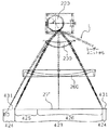
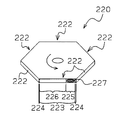
図4はレーザユニットから発光された光ビームの展開図、図5は図1から図4に示したポリゴンミラーの拡大斜視図である。
【0053】
第1の実施形態では、図5に示すように、ポリゴンミラー220の周面には、6つの反射面222が形成されている。詳細には、各反射面222には、感光体ドラム27(図1)の表面上に静電潜像を書き込むために用いられる光ビームを反射する書き込み領域223が設けられており、更に、感光体ドラム27(図1)の表面上に画像静電潜像を書き込むために用いられない光ビームを反射する非書き込み領域224が書き込み領域223の両側に設けられている。更に詳細には、書き込み領域223には、第1反射率を有する第1部分225と、第1反射率より低い第2反射率を有する第2部分226とが設けられている。
【0054】
また、第1の実施形態では、反射面222の第1部分225にコーティングされたコーティング層の厚さを第2部分226にコーティングされたコーティング層の厚さよりも薄くすることにより、第2反射率が第1反射率よりも低くなるように、レーザユニット300から発光される光ビームの偏光方向(P偏光、S偏光)、波長、レーザユニット300に対するポリゴンミラーの配置が選択されている。つまり、第1の実施形態では、第1部分225のコーティング層の厚さが比較的薄くなり、第2部分226のコーティング層の厚さが第1部分225のコーティング層の厚さよりも厚くなるように、第1部分225と第2部分226とで反射面222のコーティング層の厚さが異ならされている。具体的には、コーティング材料はSiO2、光ビームの偏光方向をP偏光、モータの回転方向を反時計回り、波長を780nmとした場合、第1部分225の膜厚は48.2nm、第2部分226の膜厚は93.5nmである。尚、第1部分225側の非書き込み領域224は、第1部分225と同一の第1反射率とされており、つまり、第1部分225と同一のコーティング層の厚さである。また、第2部分226側の非書き込み領域224は、第2部分226と同一の第2反射率とされており、つまり、第2部分226と同一のコーティング層の厚さである。
【0055】
更に、第1の実施形態では、図5に示すように、第1部分225が第2部分226よりもポリゴンミラー220の回転方向上流側に配置されている。また、ポリゴンミラー220は、その構成上、反射面222の上流側の部分に曇りが発生しやすいという特性を有するが、第1の実施形態では、曇りが発生する部分227(図5中の網掛け部分)に比較的高い第1反射率を有する第1部分225が配置されている。
【0056】
図4及び図5に示すように、反射面222の書き込み領域223で反射された光ビームLは、感光体ドラムの表面27’上の領域423に照射され、感光体ドラムの表面27’に静電潜像が形成される。また、反射面222の非書き込み領域224で反射された光ビームLは、感光体ドラムの表面27’上の領域424に照射される。詳細には、書き込み領域223の第1部分225で反射された光ビームLは、感光体ドラムの表面27’上の領域425に照射される。また、書き込み領域223の第2部分226で反射された光ビームLは、感光体ドラムの表面27’上の領域426に照射される。
【0057】
図4に示すように、感光体ドラムの表面27’上において、用紙3(図1)の両端は位置431に対応している。つまり、用紙3の両端には、画像が書き込まれない余白部分が形成されるようになっている。
【0058】
図4及び図5に示すように、ポリゴンミラー220の反射面222で反射された光ビームLは、ポリゴンミラー220の回転を感光体ドラム27(図1)及びレジストローラ12(図1)の回転と同期させるために用いられる。具体的には、反射面222の第1部分225側の非書き込み領域224で反射された光ビームLが、同期信号検出センサBDによって検出され、それにより、ポリゴンミラー220の回転と感光体ドラム27(図1)及びレジストローラ12(図1)の回転とが同期せしめられる。
【0059】
図6は感光体ドラム表面上の走査位置と感光体ドラム表面上の光ビームパワーとの関係を示した図である。図6において、横軸は感光体ドラム表面上の走査位置を示している。図6の右側が反射面222におけるポリゴンミラー220の回転方向下流側(EOS側、つまり、エンド・オブ・スキャン側)の第2部分226に対応した領域426であり、図6の左側が反射面222におけるポリゴンミラー220の回転方向上流側の第1部分225に対応した領域425である。図6において、縦軸は感光体ドラム表面上の光ビームLのパワーを示している。
【0060】
第1の実施形態では、図6に示すように、感光体ドラム表面上の光ビームLのパワーの許容範囲501が設定されている。つまり、書き込み領域223の第1部分225で反射された光ビームLが照射される領域425上の光ビームLのパワーが許容範囲501内に含まれ、かつ、第2部分226で反射された光ビームLのパワーが許容範囲501内に含まれるように、ポリゴンミラー220の反射面である第1部分225及び第2部分226が形成されている。詳細には、ポリゴンミラー220が使用される初期時において、第1部分225に対応する領域425上の光ビームLのパワーが許容範囲501の上限付近の値になり、第2部分226に対応する領域426上の光ビームLのパワーが許容範囲501の中心付近の値になるように、第1部分225及び第2部分226が形成されている。更に、第1の実施形態では、ポリゴンミラー220の寿命時間が経過した後においても、第1部分225に対応する領域425上の光ビームLのパワー及び第2部分226に対応する領域426上の光ビームLのパワーが共に許容範囲501内に含まれるように、第1部分225及び第2部分226が形成されている。尚、許容範囲501とは、光ビームによって、感光体ドラム27上に良好に静電潜像を形成することが可能な範囲である。
【0061】
更に第1の実施形態では、ポリゴンミラー220の反射面222で反射される光ビームLのスポット形状における主走査方向(図4の左右方向)の長さがその副走査方向(図4の表裏方向)の長さよりも長くされている。
【0062】
第1の実施形態によれば、図5及び図6に示したように、第1反射率を有する第1部分225と、第1反射率より低い第2反射率を有する第2部分226とが書き込み領域223に設けられている。そのため、曇りが発生する部分227を書き込み領域223として設定することにより、ポリゴンミラー220が大型化してしまうのを回避しつつ、更に、曇りが発生する部分227で反射された光ビームLのパワーが許容範囲501よりも低くならないように反射率が高い第1部分225と反射率が低い第2部分226とを書き込み領域223に設けることにより、書き込み領域223内のある部分で反射された光ビームによって書き込まれた静電潜像の質が、他の部分で反射された光ビームによって書き込まれた静電潜像の質よりも悪化してしまうのを回避することができる。よって、長期にわたり、良好な静電潜像を形成することができ、用紙3に良好な画像を形成することができる。
【0063】
また、第1の実施形態によれば、上述したように、反射率が異なる第1部分225および第2部分226を形成するために、第1部分225と第2部分226とで、反射面222にコーティングされたコーティング層の厚さが異ならされている。詳細には、所定の光ビームが発光される第1の実施形態では、反射率が高い第1部分225を形成するためにコーティング層の厚さが薄くされ、反射率が低い第2部分226を形成するためにコーティング層の厚さが厚くされる。
【0064】
また、第1の実施形態によれば、図5及び図6に示したように、第1部分225が第2部分226よりもポリゴンミラー220の回転方向上流側に配置されている。詳細には、曇りが発生する部分227に第1部分225が配置されている。そのため、曇りが発生する部分227で反射された光ビームLのパワーが許容範囲501よりも低くならないように、曇りが発生する部分227に第1部分225を配置することにより、曇りが発生する部分227で反射された光ビームLによって書き込まれた静電潜像の質が、他の部分で反射された光ビームによって書き込まれた静電潜像の質よりも悪化してしまうのを回避することができる。
【0065】
また、第1の実施形態によれば、図5及び図6に示したように、ポリゴンミラー220の初期使用時に、第1部分225で反射された光ビームLが照射される領域425上の光ビームLのパワーが許容範囲501の上限付近の値になり、第2部分226で反射された光ビームLが照射される領域426上の光ビームLのパワーが許容範囲501の中心付近の値になるように、第1部分225及び第2部分226が形成されている。そのため、ポリゴンミラー220の長期使用により第1部分225に曇りが発生したとしても、第1部分225で反射された光ビームLが照射される領域425上の光ビームLのパワーを許容範囲501の下限よりも高い値に維持することができる。
【0066】
第1の実施形態によれば、図4及び図5に示したように、反射面220で反射される光ビームLのスポット形状における主走査方向(図4の左右方向)長さがその副走査方向(図4の表裏方向)長さよりも長くされている。そのため、反射面222に入射する光ビームLが第1部分225と第2部分226との境界線を通過する時に反射面222で反射された光ビームLのパワーがステップ状に変化してしまうのを回避することができる。
【0067】
以下、本発明の画像形成装置の他の実施形態について説明する。他の実施形態の画像形成装置は、後述する点を除き、上述した第1の実施形態の画像形成装置と同様に構成されているため、第1の実施形態とほぼ同様の効果を奏することができる。
【0068】
図7は第2の実施形態のポリゴンミラーの拡大斜視図である。第2の実施形態では、図7に示すように、ポリゴンミラー1220の周面には、6つの反射面1222が形成されている。詳細には、各反射面1222には、感光体ドラム27(図1)の表面上に静電潜像を書き込むために用いられる光ビームを反射する書き込み領域1223が設けられており、更に、感光体ドラム27(図1)の表面上に画像静電潜像を書き込むために用いられない光ビームを反射する非書き込み領域1224が書き込み領域1223の両側に設けられている。更に詳細には、書き込み領域1223には、第11反射率を有する第11部分1225と、第11反射率より低い第12反射率を有する第12部分1226とが設けられている。
【0069】
また、第2の実施形態では、反射面1222の第11部分1225にコーティングされたコーティング層の厚さを第12部分1226にコーティングされたコーティング層の厚さよりも厚くすることにより、第12反射率が第11反射率よりも低くなるように、レーザユニット300から発光される光ビームの偏光方向(P偏光、S偏光)、波長、レーザユニット300に対するポリゴンミラーの配置が選択されている。つまり、第2の実施形態では、第11部分1225のコーティング層の厚さが比較的厚くなり、第12部分1226のコーティング層の厚さが第11部分1225のコーティング層の厚さよりも薄くなるように、第11部分1225と第12部分1226とで反射面1222のコーティング層の厚さが異ならされている。尚、第11部分1225側の非書き込み領域1224は、第11部分1225と同一の第11反射率とされており、つまり、第11部分1225と同一のコーティング層の厚さである。また、第12部分1226側の非書き込み領域1224は、第12部分1226と同一の第12反射率とされており、つまり、第12部分1226と同一のコーティング層の厚さである。
【0070】
更に、第2の実施形態では、図7に示すように、第11部分1225が第12部分1226よりもポリゴンミラー1220の回転方向上流側に配置されている。また、ポリゴンミラー1220は、その構成上、反射面1222の上流側の部分に曇りが発生しやすいという特性を有するが、第2の実施形態では、曇りが発生する部分1227(図7中の網掛け部分)に比較的高い第11反射率を有する第11部分1225が配置されている。
【0071】
図8は第2の実施形態の感光体ドラム表面上の走査位置と感光体ドラム表面上の光ビームパワーとの関係を示した図である。図8において、横軸は感光体ドラム表面上の走査位置を示している。図8の右側が反射面1222におけるポリゴンミラー1220の回転方向下流側(EOS側、つまり、エンド・オブ・スキャン側)の第12部分1226に対応した領域1426であり、図8の左側が反射面1222におけるポリゴンミラー1220の回転方向上流側の第11部分1225に対応した領域1425である。図8において、縦軸は感光体ドラム表面上の光ビームLのパワーを示している。
【0072】
第2の実施形態では、図8に示すように、感光体ドラム表面上の光ビームLのパワーの許容範囲501が設定されている。つまり、書き込み領域1223の第11部分1225で反射された光ビームLが照射される領域1425上の光ビームLのパワーが許容範囲501内に含まれ、かつ、第12部分1226で反射された光ビームが照射される領域1426上の光ビームLのパワーが許容範囲501内に含まれるように、ポリゴンミラー1220の反射面である第11部分1225及び第12部分1226が形成されている。詳細には、ポリゴンミラー1220が使用される初期時において、第11部分1225に対応する領域1425上の光ビームLのパワーが許容範囲501の上限付近の値になり、第12部分1226に対応する領域1426上の光ビームLのパワーが許容範囲501の中心付近の値になるように、第11部分1225及び第12部分1226が形成されている。更に、第2の実施形態では、ポリゴンミラー1220の寿命時間が経過した後においても、第11部分1225に対応する領域1425上の光ビームLのパワー及び第12部分1226に対応する領域1426上の光ビームLのパワーが共に許容範囲501内に含まれるように、第11部分1225及び第12部分1226が形成されている。
【0073】
第2の実施形態によれば、図7及び図8に示したように、第11反射率を有する第11部分1225と、第11反射率より低い第12反射率を有する第12部分1226とが書き込み領域1223に設けられている。そのため、曇りが発生する部分1227を書き込み領域1223として設定することにより、ポリゴンミラー1220が大型化してしまうのを回避しつつ、更に、曇りが発生する部分1227で反射された光ビームLのパワーが許容範囲501よりも低くならないように反射率が高い第11部分1225と反射率が低い第12部分1226とを書き込み領域1223に設けることにより、書き込み領域1223内のある部分で反射された光ビームによって書き込まれた静電潜像の質が、他の部分で反射された光ビームによって書き込まれた静電潜像の質よりも悪化してしまうのを回避することができる。よって、長期にわたり、良好な静電潜像を形成することができ、用紙3に良好な画像を形成することができる。
【0074】
また、第2の実施形態によれば、上述したように、反射率が異なる第11部分1225および第12部分1226を形成するために、第11部分1225と第12部分1226とで、反射面1222にコーティングされたコーティング層の厚さが異ならされている。詳細には、第1の実施形態とは異なる光ビームが発光される第2の実施形態では、反射率が高い第11部分1225を形成するためにコーティング層の厚さが厚くされ、反射率が低い第12部分1226を形成するためにコーティング層の厚さが薄くされる。
【0075】
また、第2の実施形態によれば、図7及び図8に示したように、第11部分1225が第12部分1226よりもポリゴンミラー1220の回転方向上流側に配置されている。詳細には、曇りが発生する部分1227に第11部分1225が配置されている。そのため、曇りが発生する部分1227で反射された光ビームLのパワーが許容範囲501よりも低くならないように、曇りが発生する部分1227に第11部分1225を配置することにより、曇りが発生する部分1227で反射された光ビームLによって書き込まれた静電潜像の質が、他の部分で反射された光ビームによって書き込まれた静電潜像の質よりも悪化してしまうのを回避することができる。
【0076】
また、第2の実施形態によれば、図7及び図8に示したように、ポリゴンミラー1220の初期使用時に、第11部分1225で反射された光ビームLが照射される領域1425上の光ビームLのパワーが許容範囲501の上限付近の値になり、第12部分1226で反射された光ビームLが照射される領域1426上の光ビームLのパワーが許容範囲501の中心付近の値になるように、第11部分1225及び第12部分1226が形成されている。そのため、ポリゴンミラー1220の長期使用により第11部分1225に曇りが発生したとしても、第11部分1225で反射された光ビームLが照射される領域1425上の光ビームLのパワーを許容範囲501の下限よりも高い値に維持することができる。
【0077】
図9は第3の実施形態のポリゴンミラーの拡大斜視図である。第3の実施形態では、図9に示すように、ポリゴンミラー2220の周面には、6つの反射面2222が形成されている。詳細には、各反射面2222には、感光体ドラム27(図1)の表面上に静電潜像を書き込むために用いられる光ビームを反射する書き込み領域2223が設けられており、更に、感光体ドラム27(図1)の表面上に静電潜像を書き込むために用いられない光ビームを反射する非書き込み領域2224が書き込み領域2223の両側に設けられている。更に詳細には、書き込み領域2223には、第21反射率を有する第21部分2225と、第21反射率より低い第22反射率を有する第22部分2226とが設けられている。
【0078】
また、第3の実施形態では、反射面2222の第21部分2225にコーティングされたコーティング層の屈折率を第22部分2226にコーティングされたコーティング層の屈折率よりも低くすることにより、第22反射率が第21反射率よりも低くなるように、レーザユニット300から発光される光ビームの偏光方向(P偏光、S偏光)、波長、レーザユニット300に対するポリゴンミラーの配置が選択されている。つまり、第3の実施形態では、第21部分2225のコーティング層の屈折率が比較的低くなり、第22部分2226のコーティング層の屈折率が第21部分2225のコーティング層の屈折率よりも高くなるように、第21部分2225と第22部分2226とで反射面2222のコーティング層の屈折率が異ならされている。尚、第21部分2225側の非書き込み領域2224は、第21部分2225と同一の第21反射率とされており、つまり、第21部分2225と同一のコーティング層の屈折率である。また、第22部分2226側の非書き込み領域2224は、第22部分2226と同一の第22反射率とされており、つまり、第22部分2226と同一のコーティング層の屈折率である。
【0079】
更に、第3の実施形態では、図9に示すように、第21部分2225が第22部分2226よりもポリゴンミラー2220の回転方向上流側に配置されている。また、ポリゴンミラー2220は、その構成上、反射面2222の上流側の部分に曇りが発生しやすいという特性を有するが、第3の実施形態では、曇りが発生する部分2227(図9中の網掛け部分)に比較的高い第21反射率を有する第21部分2225が配置されている。
【0080】
図10は第3の実施形態の感光体ドラム表面上の走査位置と感光体ドラム表面上の光ビームパワーとの関係を示した図である。図10において、横軸は感光体ドラム表面上の走査位置を示している。図10の右側が反射面2222におけるポリゴンミラー2220の回転方向下流側(EOS側、つまり、エンド・オブ・スキャン側)の第22部分2226に対応した領域2426であり、図10の左側が反射面2222におけるポリゴンミラー2220の回転方向上流側の第21部分2225に対応した領域2425である。図10において、縦軸は感光体ドラム表面上の光ビームLのパワーを示している。
【0081】
第3の実施形態では、図10に示すように、感光体ドラム表面上の光ビームLのパワーの許容範囲501が設定されている。つまり、書き込み領域2223の第21部分2225で反射された光ビームLが照射される領域1425上の光ビームLのパワーが許容範囲501内に含まれ、かつ、第22部分2226で反射された光ビームLが照射される領域1426上の光ビームLのパワーが許容範囲501内に含まれるように、ポリゴンミラー2220の反射面である第21部分2225及び第22部分2226が形成されている。詳細には、ポリゴンミラー2220が使用される初期時において、第21部分2225に対応する領域2425上の光ビームLのパワーが許容範囲501の上限付近の値になり、第22部分2226に対応する領域2426上の光ビームLのパワーが許容範囲501の中心付近の値になるように、第21部分2225及び第22部分2226が形成されている。更に、第3の実施形態では、ポリゴンミラー2220の寿命時間が経過した後においても、第21部分2225に対応する領域2425上の光ビームLのパワー及び第22部分2226に対応する領域2426上の光ビームLのパワーが共に許容範囲501内に含まれるように、第21部分2225及び第22部分2226が形成されている。
【0082】
第3の実施形態によれば、図9及び図10に示したように、第21反射率を有する第21部分2225と、第21反射率より低い第22反射率を有する第22部分2226とが書き込み領域2223に設けられている。そのため、曇りが発生する部分2227を書き込み領域2223として設定することにより、ポリゴンミラー2220が大型化してしまうのを回避しつつ、更に、曇りが発生する部分2227で反射された光ビームLのパワーが許容範囲501よりも低くならないように反射率が高い第21部分2225と反射率が低い第22部分2226とを書き込み領域2223に設けることにより、書き込み領域2223内のある部分で反射された光ビームによって書き込まれた静電潜像の質が、他の部分で反射された光ビームによって書き込まれた静電潜像の質よりも悪化してしまうのを回避することができる。よって、長期にわたり、良好な静電潜像を形成することができ、用紙3に良好な画像を形成することができる。
【0083】
また、第3の実施形態によれば、上述したように、反射率が異なる第21部分2225および第22部分2226を形成するために、第21部分2225と第22部分2226とで、反射面2222にコーティングされたコーティング層の屈折率が異ならされている。詳細には、所定の光ビームが発光される第3の実施形態では、反射率が高い第21部分2225を形成するためにコーティング層の屈折率が低くされ、反射率が低い第22部分2226を形成するためにコーティング層の屈折率が高くされる。
【0084】
また、第3の実施形態によれば、図9及び図10に示したように、第21部分2225が第22部分2226よりもポリゴンミラー2220の回転方向上流側に配置されている。詳細には、曇りが発生する部分2227に第21部分2225が配置されている。そのため、曇りが発生する部分2227で反射された光ビームLのパワーが許容範囲501よりも低くならないように、曇りが発生する部分2227に第21部分2225を配置することにより、曇りが発生する部分2227で反射された光ビームLによって書き込まれた静電潜像の質が、他の部分で反射された光ビームによって書き込まれた静電潜像の質よりも悪化してしまうのを回避することができる。
【0085】
また、第3の実施形態によれば、図9及び図10に示したように、ポリゴンミラー2220の初期使用時に、第21部分2225で反射された光ビームLが照射される領域2425上の光ビームLのパワーが許容範囲501の上限付近の値になり、第22部分2226で反射された光ビームLが照射される領域2426上の光ビームLのパワーが許容範囲501の中心付近の値になるように、第21部分2225及び第22部分2226が形成されている。そのため、ポリゴンミラー2220の長期使用により第21部分2225に曇りが発生したとしても、第21部分2225で反射された光ビームLが照射される領域2425上の光ビームLのパワーを許容範囲501の下限よりも高い値に維持することができる。
【0086】
図11は第4の実施形態のポリゴンミラーの拡大斜視図である。第4の実施形態では、図11に示すように、ポリゴンミラー3220の周面には、6つの反射面3222が形成されている。詳細には、各反射面3222には、感光体ドラム27(図1)の表面上に静電潜像を書き込むために用いられる光ビームを反射する書き込み領域3223が設けられており、更に、感光体ドラム27(図1)の表面上に静電潜像を書き込むために用いられない光ビームを反射する非書き込み領域3224が書き込み領域3223の両側に設けられている。更に詳細には、書き込み領域3223には、第31反射率を有する第31部分3225と、第31反射率より低い第32反射率を有する第32部分3226とが設けられている。
【0087】
また、第4の実施形態では、反射面3222の第31部分3225にコーティングされたコーティング層の屈折率を第32部分3226にコーティングされたコーティング層の屈折率よりも高くすることにより、第32反射率が第31反射率よりも低くなるように、レーザユニット300から発光される光ビームの偏光方向(P偏光、S偏光)、波長、入射角レーザユニット300に対するポリゴンミラーの配置が選択されている。つまり、第4の実施形態では、第31部分3225のコーティング層の屈折率が比較的高くなり、第32部分3226のコーティング層の屈折率が第31部分3225のコーティング層の屈折率よりも低くなるように、第31部分3225と第32部分3226とで反射面3222のコーティング層の屈折率が異ならされている。尚、第31部分3225側の非書き込み領域3224は、第31部分3225と同一の第31反射率とされており、つまり、第31部分3225と同一のコーティング層の屈折率である。また、第32部分3226側の非書き込み領域3224は、第32部分3226と同一の第32反射率とされており、つまり、第32部分3226と同一のコーティング層の屈折率である。
【0088】
更に、第4の実施形態では、図11に示すように、第31部分3225が第32部分3226よりもポリゴンミラー3220の回転方向上流側に配置されている。また、ポリゴンミラー3220は、その構成上、反射面3222の上流側の部分に曇りが発生しやすいという特性を有するが、第4の実施形態では、曇りが発生する部分3227(図11中の網掛け部分)に比較的高い第31反射率を有する第31部分3225が配置されている。
【0089】
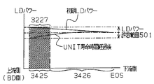
図12は第4の実施形態の感光体ドラム表面上の走査位置と感光体ドラム表面上の光ビームパワーとの関係を示した図である。図12において、横軸は感光体ドラム表面上の走査位置を示している。図12の右側が反射面3222におけるポリゴンミラー3220の回転方向下流側(EOS側、つまり、エンド・オブ・スキャン側)の第32部分3226に対応した領域3426であり、図12の左側が反射面3222におけるポリゴンミラー3220の回転方向上流側の第31部分3225に対応した領域3425である。図12において、縦軸は感光体ドラム表面上の光ビームLのパワーを示している。
【0090】
第4の実施形態では、図12に示すように、感光体ドラム表面上の光ビームLのパワーの許容範囲501が設定されている。つまり、書き込み領域3223の第31部分3225で反射された光ビームLが照射される領域3425上の光ビームLのパワーが許容範囲501内に含まれ、かつ、第32部分3226で反射された光ビームLが照射される領域3426上の光ビームLのパワーが許容範囲501内に含まれるように、ポリゴンミラー3220の反射面である第31部分3225及び第32部分3226が形成されている。詳細には、ポリゴンミラー3220が使用される初期時において、第31部分3225に対応する領域3425上の光ビームLのパワーが許容範囲501の上限付近の値になり、第32部分3226に対応する領域3426上の光ビームLのパワーが許容範囲501の中心付近の値になるように、第31部分3225及び第32部分3226が形成されている。更に、第4の実施形態では、ポリゴンミラー3220の寿命時間が経過した後においても、第31部分3225に対応する領域3425上の光ビームLのパワー及び第32部分3226に対応する領域3426上の光ビームLのパワーが共に許容範囲501内に含まれるように、第31部分3225及び第32部分3226が形成されている。
【0091】
第4の実施形態によれば、図11及び図12に示したように、第31反射率を有する第31部分3225と、第31反射率より低い第32反射率を有する第32部分3226とが書き込み領域3223に設けられている。そのため、曇りが発生する部分3227を書き込み領域3223として設定することにより、ポリゴンミラー3220が大型化してしまうのを回避しつつ、更に、曇りが発生する部分3227で反射された光ビームLのパワーが許容範囲501よりも低くならないように反射率が高い第31部分3225と反射率が低い第32部分3226とを書き込み領域3223に設けることにより、書き込み領域3223内のある部分で反射された光ビームによって書き込まれた静電潜像の質が、他の部分で反射された光ビームによって書き込まれた静電潜像の質よりも悪化してしまうのを回避することができる。よって、長期にわたり、良好な静電潜像を形成することができ、用紙3に良好な画像を形成することができる。
【0092】
また、第4の実施形態によれば、上述したように、反射率が異なる第31部分3225および第32部分3226を形成するために、第31部分3225と第32部分3226とで、反射面3222にコーティングされたコーティング層の屈折率が異ならされている。詳細には、第3の実施形態とは異なる光ビームが発光される第4の実施形態では、反射率が高い第31部分3225を形成するためにコーティング層の屈折率が高くされ、反射率が低い第32部分3226を形成するためにコーティング層の屈折率が低くされる。
【0093】
また、第4の実施形態によれば、図11及び図12に示したように、第31部分3225が第32部分3226よりもポリゴンミラー3220の回転方向上流側に配置されている。詳細には、曇りが発生する部分3227に第31部分3225が配置されている。そのため、曇りが発生する部分3227で反射された光ビームLのパワーが許容範囲501よりも低くならないように、曇りが発生する部分3227に第31部分3225を配置することにより、曇りが発生する部分3227で反射された光ビームLによって書き込まれた静電潜像の質が、他の部分で反射された光ビームによって書き込まれた静電潜像の質よりも悪化してしまうのを回避することができる。
【0094】
また、第4の実施形態によれば、図11及び図12に示したように、ポリゴンミラー3220の初期使用時に、第31部分3225で反射された光ビームLが照射される領域3425上の光ビームLのパワーが許容範囲501の上限付近の値になり、第32部分3226で反射された光ビームLが照射される領域3426上の光ビームLのパワーが許容範囲501の中心付近の値になるように、第31部分3225及び第32部分3226が形成されている。そのため、ポリゴンミラー3220の長期使用により第31部分3225に曇りが発生したとしても、第31部分3225で反射された光ビームLが照射される領域3425上の光ビームLのパワーを許容範囲501の下限よりも高い値に維持することができる。
【0095】
本発明の画像形成装置の第1から第4の実施形態について説明したが、本発明は、ポリゴンミラーがより高速で回転される画像形成装置に適用されるほど、顕著な効果を奏する。
【0096】
【発明の効果】
請求項1〜3、8、9に記載の発明によれば、ポリゴンミラーが大型化してしまうのを回避しつつ、書き込み領域内のある部分で反射された光ビームによって書き込まれた静電潜像の質が、他の部分で反射された光ビームによって書き込まれた静電潜像の質よりも悪化してしまうのを回避することができる。
【0097】
請求項4及び5に記載の発明によれば、曇りが発生する部分で反射された光ビームによって書き込まれた静電潜像の質が、他の部分で反射された光ビームによって書き込まれた静電潜像の質よりも悪化してしまうのを回避することができる。
【0098】
請求項6に記載の発明によれば、ポリゴンミラーの長期使用により曇りが発生したとしても、第1部分で反射された光ビームのパワーを許容範囲の下限よりも高い値に維持することができる。
【0099】
請求項7に記載の発明によれば、反射面に入射する光ビームが第1部分と第2部分との境界線を通過する時に反射面で反射された光ビームのパワーがステップ状に変化してしまうのを回避することができる。
【図面の簡単な説明】
【図1】本発明の画像形成装置の第1の実施形態を適用したレーザプリンタの側断面図である。
【図2】上蓋部材を外した状態で図1の右上から見たスキャナユニットの斜視図である。
【図3】上蓋部材およびトレイを外した状態で図2とは別角度から見たスキャナユニットの斜視図である。
【図4】レーザユニットから発光された光ビームの展開図である。
【図5】図1から図4に示したポリゴンミラーの拡大斜視図である。
【図6】感光体ドラム表面上の走査位置と感光体ドラム表面上の光ビームパワーとの関係を示した図である。
【図7】第2の実施形態のポリゴンミラーの拡大斜視図である。
【図8】第2の実施形態の感光体ドラム表面上の走査位置と感光体ドラム表面上の光ビームパワーとの関係を示した図である。
【図9】第3の実施形態のポリゴンミラーの拡大斜視図である。
【図10】第3の実施形態の感光体ドラム表面上の走査位置と感光体ドラム表面上の光ビームパワーとの関係を示した図である。
【図11】第4の実施形態のポリゴンミラーの拡大斜視図である。
【図12】第4の実施形態の感光体ドラム表面上の走査位置と感光体ドラム表面上の光ビームパワーとの関係を示した図である。
【符号の説明】
220…ポリゴンミラー、222…反射面、223…書き込み領域、224…非書き込み領域、225…第1部分、226…第2部分、227…曇りが発生する部分[0001]
TECHNICAL FIELD OF THE INVENTION
The present invention relates to a polygon mirror having a reflection surface for reflecting a light beam, an optical scanning device having the polygon mirror, and an image forming apparatus having the optical scanning device. The polygon mirror, the optical scanning device, and the image forming device of the present invention are applicable to, for example, a printer, a facsimile, a copying machine, and the like.
[0002]
[Prior art]
Conventionally, a reflection area for reflecting a light beam is provided, and a writing area for reflecting a light beam used for writing an electrostatic latent image and a light beam not used for writing an electrostatic latent image are reflected. Polygon mirror provided with a non-writing area for reflection on a reflection surface is known. An example of this type of polygon mirror is described in, for example, Japanese Patent Application Laid-Open No. 7-199106. In the polygon mirror described in JP-A-7-199106, as the power of a light beam reflected at a portion where fogging occurs becomes lower than a desired value, the electrostatic latent written by the light beam is reduced. In order to prevent the image quality from deteriorating, the part where the fogging occurs is set as a non-writing area, and the light beam reflected by the part where the fogging occurs is used for writing the electrostatic latent image. It is not used.
[0003]
However, when a portion where fogging occurs is set as a non-writing region as in a polygon mirror described in Japanese Patent Application Laid-Open No. 7-199106, the entire reflecting surface must be formed in order to secure a necessary and sufficient writing region. It would be necessary to increase it. That is, the polygon mirror becomes large. When the size of the polygon mirror is increased, the size of an optical scanning device, an image forming apparatus, and the like having the polygon mirror also increases.
[0004]
Conventionally, a reflection area for reflecting a light beam is provided, and a writing area for reflecting a light beam used for writing an electrostatic latent image and a light beam not used for writing an electrostatic latent image are reflected. There is known a polygon mirror provided with a non-writing area for performing the operation on a reflection surface. An example of this type of polygon mirror is described in, for example, Japanese Patent Application Laid-Open No. H11-295633. In the polygon mirror described in Japanese Patent Application Laid-Open No. H11-295633, the reflectance of the non-writing area is increased, and the reflectance of the writing area is decreased.
[0005]
However, in the polygon mirror described in JP-A-11-295633, although the reflectance of the writing area and the reflectance of the non-writing area are set to different values, JP-A-11-295633 discloses that: It does not disclose that the reflectivity differs in the writing area. Therefore, in the polygon mirror described in Japanese Patent Application Laid-Open No. H11-295633, for example, when a portion where fogging occurs is set as a writing region, an electrostatic latent image written by a light beam reflected by that portion is used. The quality may be worse than the quality of the electrostatic latent image written by the light beam reflected by other parts, which may degrade the image quality on paper.
[0006]
[Patent Document 1]
JP-A-7-199106
[0007]
[Patent Document 2]
JP-A-11-295633
[0008]
[Problems to be solved by the invention]
In view of the above problems, the present invention avoids the polygon mirror becoming large due to the fact that the portion where the fogging of the reflection surface occurs is set as the non-writing area, for example, the portion where the fogging occurs is avoided. When set as a writing area, a polygon mirror, an optical scanning device, and an image forming apparatus capable of avoiding deterioration of the quality of an electrostatic latent image written by a light beam reflected at the writing area The purpose is to provide.
[0009]
[Means for Solving the Problems]
According to the first aspect of the present invention, there is provided a reflection area for reflecting a light beam, a writing area for reflecting a light beam used for writing an electrostatic latent image, and writing of an electrostatic latent image. A polygon mirror having a non-writing area for reflecting a light beam that is not used for the first portion having a first reflectance and a second portion having a second reflectance lower than the first reflectance. A polygon mirror is provided, wherein two parts are provided in the writing area.
[0010]
In the polygon mirror according to the first aspect, the first portion having the first reflectance and the second portion having the second reflectance lower than the first reflectance are provided in the writing area. Therefore, for example, by setting a portion where fogging occurs as a writing area, it is possible to prevent the polygon mirror from being enlarged, and furthermore, for example, the power of the light beam reflected on the portion where fogging occurs is smaller than a desired value. By providing a first portion having a high reflectivity and a second portion having a low reflectivity in the writing area so as not to be lowered, the electrostatic latent image written by the light beam reflected by a certain portion in the writing area is provided. The quality can be prevented from being worse than the quality of the electrostatic latent image written by the light beam reflected by other parts.
[0011]
The polygon mirror according to claim 1, wherein the first portion and the second portion have different thicknesses of a coating layer coated on the reflection surface. Is provided.
[0012]
In the polygon mirror according to claim 2, in order to form the first portion and the second portion having different reflectivities, if the thickness of the coating layer coated on the reflection surface is different between the first portion and the second portion. Have been. In particular, for example, in some cases, the thickness of the coating layer is reduced to form a first portion with high reflectivity, and the thickness of the coating layer is increased to form a second portion with low reflectivity. Be killed. In other cases, the thickness of the coating layer is increased to form a first portion having a high reflectance, and the thickness of the coating layer is reduced to form a second portion having a low reflectance. . For example, whether to increase or decrease the thickness of the coating layer in order to increase the reflectance is determined based on, for example, the wavelength, type, incident angle, and the like of the light beam.
[0013]
The polygon mirror according to claim 1, wherein the first portion and the second portion have different refractive indexes of a coating layer coated on the reflection surface. Is provided.
[0014]
In the polygon mirror according to the third aspect, in order to form the first portion and the second portion having different reflectivities, if the refractive index of the coating layer coated on the reflection surface is different between the first portion and the second portion. Have been. In particular, for example, in some cases, the refractive index of the coating layer is reduced to form a first portion having a high reflectivity, and the refractive index of the coating layer is increased to form a second portion having a low reflectivity. Be killed. In other cases, the refractive index of the coating layer is increased to form a first portion having a high reflectivity, and the refractive index of the coating layer is decreased to form a second portion having a low reflectivity. For example, whether to increase or decrease the refractive index of the coating layer in order to increase the reflectance is determined based on, for example, the wavelength, type, incident angle, and the like of the light beam.
[0015]
According to the invention as set forth in claim 4, the first portion is disposed upstream of the second portion in the rotation direction of the polygon mirror. A polygon mirror is provided.
[0016]
According to the fifth aspect of the present invention, there is provided the polygon mirror according to any one of the first to fourth aspects, wherein the first portion is arranged at a portion where fogging occurs.
[0017]
In the polygon mirror according to claim 4 or 5, in consideration of the fact that a portion where fogging occurs is formed in a portion of the reflection surface of the polygon mirror on the upstream side in the rotation direction of the polygon mirror, the first portion is the second portion. It is arranged on the upstream side in the rotation direction of the polygon mirror. Preferably, the first portion is arranged at a portion where fogging occurs. Therefore, for example, by arranging the first portion in a portion where fogging occurs so that the power of the light beam reflected in the portion where fogging occurs does not become lower than a desired value, the light is reflected in a portion where fogging occurs It is possible to prevent the quality of the electrostatic latent image written by the light beam from being deteriorated than the quality of the electrostatic latent image written by the light beam reflected by other portions.
[0018]
According to the invention described in claim 6, a power allowable range of the light beam reflected by the writing area is provided, and the power of the light beam reflected by the first portion is set to a value near an upper limit of the power allowable range. Wherein the first portion and the second portion are formed such that the power of the light beam reflected by the second portion has a value near the center of the power allowable range. 5. A polygon mirror according to any one of the first to fifth aspects.
[0019]
In the polygon mirror according to the sixth aspect, the power of the light beam reflected by the first portion has a value near the upper limit of the allowable range, and the power of the light beam reflected by the second portion has a value near the center of the allowable range. The first portion and the second portion are formed so as to have a value. Therefore, even if the first portion foggs due to long-term use of the polygon mirror, the power of the light beam reflected by the first portion can be maintained at a value higher than the lower limit of the allowable range.
[0020]
According to the seventh aspect of the present invention, the length in the main scanning direction of the spot shape of the light beam reflected by the reflection surface is longer than the length in the sub-scanning direction. A polygon mirror according to claim 1 is provided.
[0021]
In the polygon mirror according to the seventh aspect, the length in the main scanning direction of the spot shape of the light beam reflected by the reflecting surface is longer than the length in the sub-scanning direction. Therefore, it is possible to prevent the power of the light beam reflected by the reflection surface from changing stepwise when the light beam incident on the reflection surface passes through the boundary between the first portion and the second portion. .
[0022]
According to an eighth aspect of the present invention, there is provided the polygon mirror according to any one of the first to seventh aspects, a driving unit that rotationally drives the polygon mirror, and a light emitting unit that emits a light beam. An optical scanning device is provided.
[0023]
According to the optical scanning device of the eighth aspect, a good electrostatic latent image can be formed for a long time.
[0024]
According to the ninth aspect of the present invention, an electrostatic latent image formed by the optical scanning device according to the eighth aspect and the light beam scanned by the optical scanning device is developed to form an image on a recording medium. An image forming apparatus comprising: an image forming unit that forms an image.
[0025]
In the image forming apparatus according to the ninth aspect, a good image can be formed for a long time.
[0026]
BEST MODE FOR CARRYING OUT THE INVENTION
Hereinafter, embodiments of the present invention will be described with reference to the accompanying drawings.
[0027]
FIG. 1 is a side sectional view of a laser printer to which a first embodiment of the image forming apparatus of the present invention is applied. As shown in FIG. 1, a laser printer 1 includes an
[0028]
The
[0029]
The
[0030]
The feeder unit 4 includes a
[0031]
The
[0032]
The paper dust generated by friction between the
[0033]
Above the paper cassette 6, a
[0034]
Above the double-
[0035]
The low-voltage
[0036]
The process cartridge 17 that forms a part of the image forming unit has a
[0037]
The
[0038]
The
[0039]
When the developing
[0040]
The
[0041]
The
[0042]
The
[0043]
A
[0044]
In the laser printer 1, a so-called cleanerless developing method in which after the toner is transferred from the
[0045]
The fixing
[0046]
Next, the
[0047]
As shown in FIG. 1, the housing of the
[0048]
As shown in FIG. 2, the
[0049]
On the upper layer of the
[0050]
As shown in FIG. 1, on the lower layer side of the
[0051]
As shown in FIGS. 2 and 3, a
[0052]
FIG. 4 is a developed view of a light beam emitted from the laser unit, and FIG. 5 is an enlarged perspective view of the polygon mirror shown in FIGS.
[0053]
In the first embodiment, as shown in FIG. 5, on the peripheral surface of the
[0054]
In the first embodiment, the thickness of the coating layer coated on the
[0055]
Further, in the first embodiment, as shown in FIG. 5, the
[0056]
As shown in FIGS. 4 and 5, the light beam L reflected by the writing area 223 of the
[0057]
As shown in FIG. 4, both ends of the sheet 3 (FIG. 1) correspond to
[0058]
As shown in FIGS. 4 and 5, the light beam L reflected by the
[0059]
FIG. 6 is a diagram showing the relationship between the scanning position on the photosensitive drum surface and the light beam power on the photosensitive drum surface. In FIG. 6, the horizontal axis indicates the scanning position on the surface of the photosensitive drum. The right side of FIG. 6 is an
[0060]
In the first embodiment, as shown in FIG. 6, an allowable range 501 of the power of the light beam L on the surface of the photosensitive drum is set. That is, the power of the light beam L on the
[0061]
Further, in the first embodiment, the length of the spot shape of the light beam L reflected by the
[0062]
According to the first embodiment, as shown in FIGS. 5 and 6, the
[0063]
Further, according to the first embodiment, as described above, in order to form the
[0064]
Further, according to the first embodiment, as shown in FIGS. 5 and 6, the
[0065]
Further, according to the first embodiment, as shown in FIGS. 5 and 6, when the
[0066]
According to the first embodiment, as shown in FIG. 4 and FIG. 5, the length of the spot shape of the light beam L reflected by the reflecting
[0067]
Hereinafter, another embodiment of the image forming apparatus of the present invention will be described. The image forming apparatus according to the other embodiment is configured in the same manner as the image forming apparatus according to the above-described first embodiment, except for the points described below, and thus can provide substantially the same effects as those of the first embodiment. it can.
[0068]
FIG. 7 is an enlarged perspective view of the polygon mirror according to the second embodiment. In the second embodiment, as shown in FIG. 7, on the peripheral surface of the
[0069]
In the second embodiment, the thickness of the coating layer coated on the
[0070]
Further, in the second embodiment, as shown in FIG. 7, the
[0071]
FIG. 8 is a diagram showing the relationship between the scanning position on the photosensitive drum surface and the light beam power on the photosensitive drum surface according to the second embodiment. In FIG. 8, the horizontal axis indicates the scanning position on the surface of the photosensitive drum. The right side of FIG. 8 is an
[0072]
In the second embodiment, as shown in FIG. 8, an allowable range 501 of the power of the light beam L on the surface of the photosensitive drum is set. That is, the power of the light beam L on the area 1425 to which the light beam L reflected by the
[0073]
According to the second embodiment, as shown in FIGS. 7 and 8, the
[0074]
Further, according to the second embodiment, as described above, in order to form the
[0075]
According to the second embodiment, as shown in FIGS. 7 and 8, the
[0076]
According to the second embodiment, as shown in FIGS. 7 and 8, when the
[0077]
FIG. 9 is an enlarged perspective view of the polygon mirror according to the third embodiment. In the third embodiment, as shown in FIG. 9, six reflecting
[0078]
Further, in the third embodiment, the refractive index of the coating layer coated on the
[0079]
Further, in the third embodiment, as shown in FIG. 9, the
[0080]
FIG. 10 is a diagram showing the relationship between the scanning position on the photosensitive drum surface and the light beam power on the photosensitive drum surface according to the third embodiment. In FIG. 10, the horizontal axis indicates the scanning position on the surface of the photosensitive drum. The right side of FIG. 10 is an
[0081]
In the third embodiment, as shown in FIG. 10, an allowable range 501 of the power of the light beam L on the surface of the photosensitive drum is set. That is, the power of the light beam L on the area 1425 irradiated with the light beam L reflected by the
[0082]
According to the third embodiment, as shown in FIGS. 9 and 10, the
[0083]
Further, according to the third embodiment, as described above, in order to form the
[0084]
According to the third embodiment, as shown in FIGS. 9 and 10, the twenty-
[0085]
According to the third embodiment, as shown in FIGS. 9 and 10, when the
[0086]
FIG. 11 is an enlarged perspective view of the polygon mirror according to the fourth embodiment. In the fourth embodiment, as shown in FIG. 11, six reflecting
[0087]
In the fourth embodiment, the refractive index of the coating layer coated on the
[0088]
Further, in the fourth embodiment, as shown in FIG. 11, the
[0089]
FIG. 12 is a diagram showing the relationship between the scanning position on the photosensitive drum surface and the light beam power on the photosensitive drum surface according to the fourth embodiment. In FIG. 12, the horizontal axis indicates the scanning position on the surface of the photosensitive drum. The right side of FIG. 12 is an
[0090]
In the fourth embodiment, as shown in FIG. 12, an allowable range 501 of the power of the light beam L on the surface of the photosensitive drum is set. That is, the power of the light beam L on the
[0091]
According to the fourth embodiment, as shown in FIGS. 11 and 12, the
[0092]
According to the fourth embodiment, as described above, in order to form the
[0093]
Further, according to the fourth embodiment, as shown in FIGS. 11 and 12, the
[0094]
Further, according to the fourth embodiment, as shown in FIGS. 11 and 12, when the
[0095]
Although the first to fourth embodiments of the image forming apparatus of the present invention have been described, the present invention has a more remarkable effect as applied to an image forming apparatus in which a polygon mirror is rotated at a higher speed.
[0096]
【The invention's effect】
According to the present invention, the electrostatic latent image written by the light beam reflected by a certain portion in the writing area is avoided while preventing the polygon mirror from being enlarged. Can be prevented from deteriorating the quality of the electrostatic latent image written by the light beam reflected by other portions.
[0097]
According to the fourth and fifth aspects of the present invention, the quality of the electrostatic latent image written by the light beam reflected by the portion where fogging occurs is improved by the static latent image written by the light beam reflected by other portions. It is possible to avoid deterioration of the quality of the latent image.
[0098]
According to the sixth aspect of the present invention, the power of the light beam reflected by the first portion can be maintained at a value higher than the lower limit of the allowable range even if the polygon mirror becomes fogged due to long-term use. .
[0099]
According to the seventh aspect of the invention, when the light beam incident on the reflecting surface passes through the boundary between the first portion and the second portion, the power of the light beam reflected on the reflecting surface changes stepwise. Can be avoided.
[Brief description of the drawings]
FIG. 1 is a side sectional view of a laser printer to which a first embodiment of an image forming apparatus according to the present invention is applied.
FIG. 2 is a perspective view of the scanner unit viewed from the upper right in FIG. 1 with an upper lid member removed.
FIG. 3 is a perspective view of the scanner unit viewed from a different angle from FIG. 2 with an upper lid member and a tray removed.
FIG. 4 is a developed view of a light beam emitted from a laser unit.
FIG. 5 is an enlarged perspective view of the polygon mirror shown in FIGS. 1 to 4;
FIG. 6 is a diagram illustrating a relationship between a scanning position on the surface of the photosensitive drum and a light beam power on the surface of the photosensitive drum.
FIG. 7 is an enlarged perspective view of a polygon mirror according to a second embodiment.
FIG. 8 is a diagram illustrating a relationship between a scanning position on a photosensitive drum surface and a light beam power on the photosensitive drum surface according to the second embodiment.
FIG. 9 is an enlarged perspective view of a polygon mirror according to a third embodiment.
FIG. 10 is a diagram illustrating a relationship between a scanning position on the photosensitive drum surface and a light beam power on the photosensitive drum surface according to the third embodiment.
FIG. 11 is an enlarged perspective view of a polygon mirror according to a fourth embodiment.
FIG. 12 is a diagram illustrating a relationship between a scanning position on a photosensitive drum surface and a light beam power on the photosensitive drum surface according to a fourth embodiment.
[Explanation of symbols]
220: polygon mirror, 222: reflection surface, 223: writing area, 224: non-writing area, 225: first part, 226 ... second part, 227: part where fogging occurs
Claims (9)
Priority Applications (2)
| Application Number | Priority Date | Filing Date | Title |
|---|---|---|---|
| JP2003020733A JP4089450B2 (en) | 2003-01-29 | 2003-01-29 | Polygon mirror, optical scanning device, and image forming apparatus |
| US10/759,089 US7054047B2 (en) | 2003-01-29 | 2004-01-20 | Polygon mirror and optical scanning device having the same |
Applications Claiming Priority (1)
| Application Number | Priority Date | Filing Date | Title |
|---|---|---|---|
| JP2003020733A JP4089450B2 (en) | 2003-01-29 | 2003-01-29 | Polygon mirror, optical scanning device, and image forming apparatus |
Publications (2)
| Publication Number | Publication Date |
|---|---|
| JP2004233554A true JP2004233554A (en) | 2004-08-19 |
| JP4089450B2 JP4089450B2 (en) | 2008-05-28 |
Family
ID=32732870
Family Applications (1)
| Application Number | Title | Priority Date | Filing Date |
|---|---|---|---|
| JP2003020733A Expired - Fee Related JP4089450B2 (en) | 2003-01-29 | 2003-01-29 | Polygon mirror, optical scanning device, and image forming apparatus |
Country Status (2)
| Country | Link |
|---|---|
| US (1) | US7054047B2 (en) |
| JP (1) | JP4089450B2 (en) |
Cited By (4)
| Publication number | Priority date | Publication date | Assignee | Title |
|---|---|---|---|---|
| JP2006091544A (en) * | 2004-09-24 | 2006-04-06 | Fuji Xerox Co Ltd | Optical scanner |
| JP2010069668A (en) * | 2008-09-17 | 2010-04-02 | Ricoh Co Ltd | Image forming device |
| JP2017049423A (en) * | 2015-09-01 | 2017-03-09 | パイオニア株式会社 | Optical element and optical element manufacturing method |
| JP2020024424A (en) * | 2019-09-26 | 2020-02-13 | パイオニア株式会社 | Optical element |
Families Citing this family (3)
| Publication number | Priority date | Publication date | Assignee | Title |
|---|---|---|---|---|
| JP4568579B2 (en) * | 2004-10-29 | 2010-10-27 | 富士通株式会社 | Light switch |
| CN100346191C (en) * | 2006-01-18 | 2007-10-31 | 河北工业大学 | Rotating mirror device with curved surface for laser scanner |
| JP7641747B2 (en) * | 2021-01-22 | 2025-03-07 | キヤノン株式会社 | Polyhedral mirror |
Family Cites Families (6)
| Publication number | Priority date | Publication date | Assignee | Title |
|---|---|---|---|---|
| JPH04106516A (en) | 1990-08-27 | 1992-04-08 | Brother Ind Ltd | scanning exposure device |
| US5151586A (en) * | 1990-08-01 | 1992-09-29 | Brother Kogyo Kabushiki Kaisha | Scanning exposure device provided with intensity correction to compensate for scan angle |
| JPH05289011A (en) | 1992-04-14 | 1993-11-05 | Fuji Photo Film Co Ltd | Image recorder |
| JPH0784201A (en) | 1993-09-17 | 1995-03-31 | Fuji Photo Film Co Ltd | Exposure device and light receiving device |
| JPH07199106A (en) | 1993-12-30 | 1995-08-04 | Canon Inc | Deflection scanning device |
| JPH11295633A (en) | 1998-04-08 | 1999-10-29 | Asahi Optical Co Ltd | Rotating polygon mirror and scanning optical device using the same |
-
2003
- 2003-01-29 JP JP2003020733A patent/JP4089450B2/en not_active Expired - Fee Related
-
2004
- 2004-01-20 US US10/759,089 patent/US7054047B2/en not_active Expired - Lifetime
Cited By (4)
| Publication number | Priority date | Publication date | Assignee | Title |
|---|---|---|---|---|
| JP2006091544A (en) * | 2004-09-24 | 2006-04-06 | Fuji Xerox Co Ltd | Optical scanner |
| JP2010069668A (en) * | 2008-09-17 | 2010-04-02 | Ricoh Co Ltd | Image forming device |
| JP2017049423A (en) * | 2015-09-01 | 2017-03-09 | パイオニア株式会社 | Optical element and optical element manufacturing method |
| JP2020024424A (en) * | 2019-09-26 | 2020-02-13 | パイオニア株式会社 | Optical element |
Also Published As
| Publication number | Publication date |
|---|---|
| US7054047B2 (en) | 2006-05-30 |
| JP4089450B2 (en) | 2008-05-28 |
| US20040145791A1 (en) | 2004-07-29 |
Similar Documents
| Publication | Publication Date | Title |
|---|---|---|
| KR20020050711A (en) | Image forming apparatus and process cartridge detachably attachable to the same | |
| JP2004069884A (en) | Image forming apparatus having image reading means | |
| JP4089450B2 (en) | Polygon mirror, optical scanning device, and image forming apparatus | |
| US7020405B2 (en) | Image forming device capable of interrupting application of driving signal at a drive unit | |
| US6750997B2 (en) | Scanning device and image forming apparatus | |
| US7400338B2 (en) | Image forming apparatus with temperature detection | |
| EP0869407A2 (en) | Image forming apparatus and cartridge removably mountable on the same | |
| JP4656877B2 (en) | Static eliminator | |
| US7184685B2 (en) | Image forming apparatus and process cartridge | |
| JP3778139B2 (en) | Temperature detector, thermal fixing device, and image forming apparatus | |
| JPH11327288A (en) | Image forming device | |
| JP4111101B2 (en) | Paper transport device and image forming apparatus provided with the paper transport device | |
| JP3837815B2 (en) | Developing device and image forming apparatus | |
| JP2003066797A (en) | Image forming apparatus and process cartridge | |
| JPH1152705A (en) | Image forming device | |
| JPH1152609A (en) | Image forming device | |
| JPH11282243A (en) | Image forming device | |
| JPH09160379A (en) | Image forming device | |
| JPH11282240A (en) | Image forming device | |
| JPH11327291A (en) | Image forming device | |
| JPH11119618A (en) | Image forming device | |
| JPH09185231A (en) | Image forming device | |
| JPH11147642A (en) | Sheet support and image forming apparatus | |
| JPH1152704A (en) | Image forming device | |
| JPH1195540A (en) | Image forming device |
Legal Events
| Date | Code | Title | Description |
|---|---|---|---|
| A621 | Written request for application examination |
Free format text: JAPANESE INTERMEDIATE CODE: A621 Effective date: 20050317 |
|
| RD07 | Notification of extinguishment of power of attorney |
Free format text: JAPANESE INTERMEDIATE CODE: A7427 Effective date: 20060824 |
|
| RD07 | Notification of extinguishment of power of attorney |
Free format text: JAPANESE INTERMEDIATE CODE: A7427 Effective date: 20060905 |
|
| TRDD | Decision of grant or rejection written | ||
| A977 | Report on retrieval |
Free format text: JAPANESE INTERMEDIATE CODE: A971007 Effective date: 20080131 |
|
| A01 | Written decision to grant a patent or to grant a registration (utility model) |
Free format text: JAPANESE INTERMEDIATE CODE: A01 Effective date: 20080205 |
|
| A61 | First payment of annual fees (during grant procedure) |
Free format text: JAPANESE INTERMEDIATE CODE: A61 Effective date: 20080218 |
|
| R150 | Certificate of patent or registration of utility model |
Ref document number: 4089450 Country of ref document: JP Free format text: JAPANESE INTERMEDIATE CODE: R150 Free format text: JAPANESE INTERMEDIATE CODE: R150 |
|
| FPAY | Renewal fee payment (event date is renewal date of database) |
Free format text: PAYMENT UNTIL: 20110307 Year of fee payment: 3 |
|
| FPAY | Renewal fee payment (event date is renewal date of database) |
Free format text: PAYMENT UNTIL: 20120307 Year of fee payment: 4 |
|
| FPAY | Renewal fee payment (event date is renewal date of database) |
Free format text: PAYMENT UNTIL: 20120307 Year of fee payment: 4 |
|
| FPAY | Renewal fee payment (event date is renewal date of database) |
Free format text: PAYMENT UNTIL: 20130307 Year of fee payment: 5 |
|
| FPAY | Renewal fee payment (event date is renewal date of database) |
Free format text: PAYMENT UNTIL: 20130307 Year of fee payment: 5 |
|
| FPAY | Renewal fee payment (event date is renewal date of database) |
Free format text: PAYMENT UNTIL: 20140307 Year of fee payment: 6 |
|
| LAPS | Cancellation because of no payment of annual fees |