JP2004234011A - 有機発光ダイオード(oled)表示装置 - Google Patents
有機発光ダイオード(oled)表示装置 Download PDFInfo
- Publication number
- JP2004234011A JP2004234011A JP2004023121A JP2004023121A JP2004234011A JP 2004234011 A JP2004234011 A JP 2004234011A JP 2004023121 A JP2004023121 A JP 2004023121A JP 2004023121 A JP2004023121 A JP 2004023121A JP 2004234011 A JP2004234011 A JP 2004234011A
- Authority
- JP
- Japan
- Prior art keywords
- light emitting
- display
- display device
- oled
- current
- Prior art date
- Legal status (The legal status is an assumption and is not a legal conclusion. Google has not performed a legal analysis and makes no representation as to the accuracy of the status listed.)
- Withdrawn
Links
- 238000012937 correction Methods 0.000 claims abstract description 57
- 230000003213 activating effect Effects 0.000 claims abstract description 4
- 230000001419 dependent effect Effects 0.000 claims 1
- 230000036962 time dependent Effects 0.000 claims 1
- 238000000034 method Methods 0.000 abstract description 28
- 230000032683 aging Effects 0.000 abstract description 17
- 239000000463 material Substances 0.000 description 46
- 239000010410 layer Substances 0.000 description 40
- -1 zinc selenide Chemical class 0.000 description 19
- 230000008859 change Effects 0.000 description 14
- 150000001875 compounds Chemical class 0.000 description 12
- 239000002019 doping agent Substances 0.000 description 12
- 239000003086 colorant Substances 0.000 description 10
- 229910052751 metal Inorganic materials 0.000 description 10
- 239000002184 metal Substances 0.000 description 10
- 239000000758 substrate Substances 0.000 description 10
- 230000007423 decrease Effects 0.000 description 9
- 238000004364 calculation method Methods 0.000 description 8
- 230000005525 hole transport Effects 0.000 description 8
- 238000002347 injection Methods 0.000 description 8
- 239000007924 injection Substances 0.000 description 8
- 239000011368 organic material Substances 0.000 description 8
- MCJGNVYPOGVAJF-UHFFFAOYSA-N quinolin-8-ol Chemical compound C1=CN=C2C(O)=CC=CC2=C1 MCJGNVYPOGVAJF-UHFFFAOYSA-N 0.000 description 8
- 229920000642 polymer Polymers 0.000 description 7
- 230000008569 process Effects 0.000 description 7
- 239000007983 Tris buffer Substances 0.000 description 6
- 230000006870 function Effects 0.000 description 6
- 239000011159 matrix material Substances 0.000 description 6
- 238000005259 measurement Methods 0.000 description 6
- 239000012044 organic layer Substances 0.000 description 6
- 239000010406 cathode material Substances 0.000 description 5
- 239000004020 conductor Substances 0.000 description 5
- 238000013461 design Methods 0.000 description 5
- 230000002431 foraging effect Effects 0.000 description 5
- 239000010409 thin film Substances 0.000 description 5
- 238000005229 chemical vapour deposition Methods 0.000 description 4
- 230000004044 response Effects 0.000 description 4
- 238000012546 transfer Methods 0.000 description 4
- SIKJAQJRHWYJAI-UHFFFAOYSA-N Indole Chemical class C1=CC=C2NC=CC2=C1 SIKJAQJRHWYJAI-UHFFFAOYSA-N 0.000 description 3
- 229910052782 aluminium Inorganic materials 0.000 description 3
- XAGFODPZIPBFFR-UHFFFAOYSA-N aluminium Chemical compound [Al] XAGFODPZIPBFFR-UHFFFAOYSA-N 0.000 description 3
- REDXJYDRNCIFBQ-UHFFFAOYSA-N aluminium(3+) Chemical compound [Al+3] REDXJYDRNCIFBQ-UHFFFAOYSA-N 0.000 description 3
- 239000010405 anode material Substances 0.000 description 3
- 230000015556 catabolic process Effects 0.000 description 3
- 238000006731 degradation reaction Methods 0.000 description 3
- 238000000151 deposition Methods 0.000 description 3
- 238000010586 diagram Methods 0.000 description 3
- 230000000694 effects Effects 0.000 description 3
- 229910052738 indium Inorganic materials 0.000 description 3
- APFVFJFRJDLVQX-UHFFFAOYSA-N indium atom Chemical compound [In] APFVFJFRJDLVQX-UHFFFAOYSA-N 0.000 description 3
- 239000000203 mixture Substances 0.000 description 3
- 229910052757 nitrogen Inorganic materials 0.000 description 3
- 229960003540 oxyquinoline Drugs 0.000 description 3
- 238000004544 sputter deposition Methods 0.000 description 3
- 239000005725 8-Hydroxyquinoline Substances 0.000 description 2
- 238000012935 Averaging Methods 0.000 description 2
- GYHNNYVSQQEPJS-UHFFFAOYSA-N Gallium Chemical compound [Ga] GYHNNYVSQQEPJS-UHFFFAOYSA-N 0.000 description 2
- KDLHZDBZIXYQEI-UHFFFAOYSA-N Palladium Chemical compound [Pd] KDLHZDBZIXYQEI-UHFFFAOYSA-N 0.000 description 2
- 229920001609 Poly(3,4-ethylenedioxythiophene) Polymers 0.000 description 2
- VYPSYNLAJGMNEJ-UHFFFAOYSA-N Silicium dioxide Chemical compound O=[Si]=O VYPSYNLAJGMNEJ-UHFFFAOYSA-N 0.000 description 2
- QCWXUUIWCKQGHC-UHFFFAOYSA-N Zirconium Chemical compound [Zr] QCWXUUIWCKQGHC-UHFFFAOYSA-N 0.000 description 2
- 150000001454 anthracenes Chemical class 0.000 description 2
- 150000004982 aromatic amines Chemical class 0.000 description 2
- 230000000903 blocking effect Effects 0.000 description 2
- OSGAYBCDTDRGGQ-UHFFFAOYSA-L calcium sulfate Chemical compound [Ca+2].[O-]S([O-])(=O)=O OSGAYBCDTDRGGQ-UHFFFAOYSA-L 0.000 description 2
- 238000006243 chemical reaction Methods 0.000 description 2
- 239000000975 dye Substances 0.000 description 2
- 238000005401 electroluminescence Methods 0.000 description 2
- 238000005538 encapsulation Methods 0.000 description 2
- 230000008020 evaporation Effects 0.000 description 2
- 238000001704 evaporation Methods 0.000 description 2
- 239000010408 film Substances 0.000 description 2
- 229910052733 gallium Inorganic materials 0.000 description 2
- 239000011777 magnesium Substances 0.000 description 2
- 238000004519 manufacturing process Methods 0.000 description 2
- 229910044991 metal oxide Inorganic materials 0.000 description 2
- 150000004706 metal oxides Chemical class 0.000 description 2
- 230000003287 optical effect Effects 0.000 description 2
- BASFCYQUMIYNBI-UHFFFAOYSA-N platinum Chemical compound [Pt] BASFCYQUMIYNBI-UHFFFAOYSA-N 0.000 description 2
- 229920003227 poly(N-vinyl carbazole) Polymers 0.000 description 2
- 229920000553 poly(phenylenevinylene) Polymers 0.000 description 2
- 150000003384 small molecules Chemical class 0.000 description 2
- 239000002904 solvent Substances 0.000 description 2
- 238000003860 storage Methods 0.000 description 2
- 230000002123 temporal effect Effects 0.000 description 2
- 125000005259 triarylamine group Chemical group 0.000 description 2
- 229910052726 zirconium Inorganic materials 0.000 description 2
- PFNQVRZLDWYSCW-UHFFFAOYSA-N (fluoren-9-ylideneamino) n-naphthalen-1-ylcarbamate Chemical compound C12=CC=CC=C2C2=CC=CC=C2C1=NOC(=O)NC1=CC=CC2=CC=CC=C12 PFNQVRZLDWYSCW-UHFFFAOYSA-N 0.000 description 1
- JYEUMXHLPRZUAT-UHFFFAOYSA-N 1,2,3-triazine Chemical compound C1=CN=NN=C1 JYEUMXHLPRZUAT-UHFFFAOYSA-N 0.000 description 1
- XNCMQRWVMWLODV-UHFFFAOYSA-N 1-phenylbenzimidazole Chemical compound C1=NC2=CC=CC=C2N1C1=CC=CC=C1 XNCMQRWVMWLODV-UHFFFAOYSA-N 0.000 description 1
- HONWGFNQCPRRFM-UHFFFAOYSA-N 2-n-(3-methylphenyl)-1-n,1-n,2-n-triphenylbenzene-1,2-diamine Chemical compound CC1=CC=CC(N(C=2C=CC=CC=2)C=2C(=CC=CC=2)N(C=2C=CC=CC=2)C=2C=CC=CC=2)=C1 HONWGFNQCPRRFM-UHFFFAOYSA-N 0.000 description 1
- KYGSXEYUWRFVNY-UHFFFAOYSA-N 2-pyran-2-ylidenepropanedinitrile Chemical class N#CC(C#N)=C1OC=CC=C1 KYGSXEYUWRFVNY-UHFFFAOYSA-N 0.000 description 1
- GOLORTLGFDVFDW-UHFFFAOYSA-N 3-(1h-benzimidazol-2-yl)-7-(diethylamino)chromen-2-one Chemical compound C1=CC=C2NC(C3=CC4=CC=C(C=C4OC3=O)N(CC)CC)=NC2=C1 GOLORTLGFDVFDW-UHFFFAOYSA-N 0.000 description 1
- CINYXYWQPZSTOT-UHFFFAOYSA-N 3-[3-[3,5-bis(3-pyridin-3-ylphenyl)phenyl]phenyl]pyridine Chemical compound C1=CN=CC(C=2C=C(C=CC=2)C=2C=C(C=C(C=2)C=2C=C(C=CC=2)C=2C=NC=CC=2)C=2C=C(C=CC=2)C=2C=NC=CC=2)=C1 CINYXYWQPZSTOT-UHFFFAOYSA-N 0.000 description 1
- MAGFQRLKWCCTQJ-UHFFFAOYSA-M 4-ethenylbenzenesulfonate Chemical compound [O-]S(=O)(=O)C1=CC=C(C=C)C=C1 MAGFQRLKWCCTQJ-UHFFFAOYSA-M 0.000 description 1
- HOEOVAJYEQMKPZ-UHFFFAOYSA-N 4-methyl-n-[4-[1-[4-(4-methyl-n-(4-methylphenyl)anilino)phenyl]cyclohexyl]phenyl]-n-(4-methylphenyl)aniline;4-methyl-n-[4-[1-[4-(4-methyl-n-(4-methylphenyl)anilino)phenyl]-4-phenylcyclohexyl]phenyl]-n-(4-methylphenyl)aniline Chemical compound C1=CC(C)=CC=C1N(C=1C=CC(=CC=1)C1(CCCCC1)C=1C=CC(=CC=1)N(C=1C=CC(C)=CC=1)C=1C=CC(C)=CC=1)C1=CC=C(C)C=C1.C1=CC(C)=CC=C1N(C=1C=CC(=CC=1)C1(CCC(CC1)C=1C=CC=CC=1)C=1C=CC(=CC=1)N(C=1C=CC(C)=CC=1)C=1C=CC(C)=CC=1)C1=CC=C(C)C=C1 HOEOVAJYEQMKPZ-UHFFFAOYSA-N 0.000 description 1
- DIVZFUBWFAOMCW-UHFFFAOYSA-N 4-n-(3-methylphenyl)-1-n,1-n-bis[4-(n-(3-methylphenyl)anilino)phenyl]-4-n-phenylbenzene-1,4-diamine Chemical compound CC1=CC=CC(N(C=2C=CC=CC=2)C=2C=CC(=CC=2)N(C=2C=CC(=CC=2)N(C=2C=CC=CC=2)C=2C=C(C)C=CC=2)C=2C=CC(=CC=2)N(C=2C=CC=CC=2)C=2C=C(C)C=CC=2)=C1 DIVZFUBWFAOMCW-UHFFFAOYSA-N 0.000 description 1
- VIZUPBYFLORCRA-UHFFFAOYSA-N 9,10-dinaphthalen-2-ylanthracene Chemical compound C12=CC=CC=C2C(C2=CC3=CC=CC=C3C=C2)=C(C=CC=C2)C2=C1C1=CC=C(C=CC=C2)C2=C1 VIZUPBYFLORCRA-UHFFFAOYSA-N 0.000 description 1
- GJCOSYZMQJWQCA-UHFFFAOYSA-N 9H-xanthene Chemical compound C1=CC=C2CC3=CC=CC=C3OC2=C1 GJCOSYZMQJWQCA-UHFFFAOYSA-N 0.000 description 1
- 229910001316 Ag alloy Inorganic materials 0.000 description 1
- KAKZBPTYRLMSJV-UHFFFAOYSA-N Butadiene Chemical class C=CC=C KAKZBPTYRLMSJV-UHFFFAOYSA-N 0.000 description 1
- QKJSGLCBKHWFBV-UHFFFAOYSA-N C1(=CC=CC2=CC=CC=C12)N(C1=CC2=CC=CC=C2C=C1)C1=CC2=CC=C(C=C2C=C1)N(C1=CC=CC2=CC=CC=C12)C1=CC2=CC=CC=C2C=C1.C1(=CC=CC2=CC=CC=C12)N(C1=CC2=CC=C(C=C2C=C1)N(C1=CC=CC2=CC=CC=C12)C1=CC=CC2=CC=CC=C12)C1=CC=CC2=CC=CC=C12.C1(=CC=C(C=C1)N(C1=CC2=CC=C(C=C2C=C1)N(C1=CC=C(C=C1)C)C1=CC=C(C=C1)C)C1=CC=C(C=C1)C)C.C1(=CC=CC=C1)C1=CC=CC=C1 Chemical compound C1(=CC=CC2=CC=CC=C12)N(C1=CC2=CC=CC=C2C=C1)C1=CC2=CC=C(C=C2C=C1)N(C1=CC=CC2=CC=CC=C12)C1=CC2=CC=CC=C2C=C1.C1(=CC=CC2=CC=CC=C12)N(C1=CC2=CC=C(C=C2C=C1)N(C1=CC=CC2=CC=CC=C12)C1=CC=CC2=CC=CC=C12)C1=CC=CC2=CC=CC=C12.C1(=CC=C(C=C1)N(C1=CC2=CC=C(C=C2C=C1)N(C1=CC=C(C=C1)C)C1=CC=C(C=C1)C)C1=CC=C(C=C1)C)C.C1(=CC=CC=C1)C1=CC=CC=C1 QKJSGLCBKHWFBV-UHFFFAOYSA-N 0.000 description 1
- BRXJHKLIGJBQSK-UHFFFAOYSA-N C1(=CC=CC2=CC=CC=C12)N(C1=CC=CC=C1)C1=CC=CC2=C(C=CC=C12)N(C1=CC=CC2=CC=CC=C12)C1=CC=CC=C1.C1=CC=CC=2C3=CC=CC=C3CC12 Chemical compound C1(=CC=CC2=CC=CC=C12)N(C1=CC=CC=C1)C1=CC=CC2=C(C=CC=C12)N(C1=CC=CC2=CC=CC=C12)C1=CC=CC=C1.C1=CC=CC=2C3=CC=CC=C3CC12 BRXJHKLIGJBQSK-UHFFFAOYSA-N 0.000 description 1
- MIGMQMUBYHNJAR-UHFFFAOYSA-N C1=C(C=C2C=CC=C3C4=CC=CC5=CC=CC(C1=C23)=C45)N(C4=CC=CC=C4)C4=CC=C(C=C4)C4=CC=C(C=C4)N(C4=CC=5C=2C=CC=C3C=CC=C(C1=CC=CC(=C4)C15)C32)C3=CC=CC=C3.C3=C(C=CC2=CC1=CC5=CC=CC=C5C=C1C=C32)N(C3=CC=CC=C3)C3=CC=C(C=C3)C3=CC=C(C=C3)N(C3=CC2=CC1=CC5=CC=CC=C5C=C1C=C2C=C3)C3=CC=CC=C3.C3=C(C=C2C=CC1=CC=CC5=CC=C3C2=C15)N(C1=CC=CC=C1)C1=CC=C(C=C1)C1=CC=C(C=C1)N(C1=CC5=CC=C2C=CC=C3C=CC(=C1)C5=C32)C3=CC=CC=C3.C3(=CC=CC=C3)C3=CC=CC=C3 Chemical group C1=C(C=C2C=CC=C3C4=CC=CC5=CC=CC(C1=C23)=C45)N(C4=CC=CC=C4)C4=CC=C(C=C4)C4=CC=C(C=C4)N(C4=CC=5C=2C=CC=C3C=CC=C(C1=CC=CC(=C4)C15)C32)C3=CC=CC=C3.C3=C(C=CC2=CC1=CC5=CC=CC=C5C=C1C=C32)N(C3=CC=CC=C3)C3=CC=C(C=C3)C3=CC=C(C=C3)N(C3=CC2=CC1=CC5=CC=CC=C5C=C1C=C2C=C3)C3=CC=CC=C3.C3=C(C=C2C=CC1=CC=CC5=CC=C3C2=C15)N(C1=CC=CC=C1)C1=CC=C(C=C1)C1=CC=C(C=C1)N(C1=CC5=CC=C2C=CC=C3C=CC(=C1)C5=C32)C3=CC=CC=C3.C3(=CC=CC=C3)C3=CC=CC=C3 MIGMQMUBYHNJAR-UHFFFAOYSA-N 0.000 description 1
- 229910002601 GaN Inorganic materials 0.000 description 1
- JMASRVWKEDWRBT-UHFFFAOYSA-N Gallium nitride Chemical compound [Ga]#N JMASRVWKEDWRBT-UHFFFAOYSA-N 0.000 description 1
- UFHFLCQGNIYNRP-UHFFFAOYSA-N Hydrogen Chemical compound [H][H] UFHFLCQGNIYNRP-UHFFFAOYSA-N 0.000 description 1
- WHXSMMKQMYFTQS-UHFFFAOYSA-N Lithium Chemical compound [Li] WHXSMMKQMYFTQS-UHFFFAOYSA-N 0.000 description 1
- FYYHWMGAXLPEAU-UHFFFAOYSA-N Magnesium Chemical compound [Mg] FYYHWMGAXLPEAU-UHFFFAOYSA-N 0.000 description 1
- JLVVSXFLKOJNIY-UHFFFAOYSA-N Magnesium ion Chemical compound [Mg+2] JLVVSXFLKOJNIY-UHFFFAOYSA-N 0.000 description 1
- ZOKXTWBITQBERF-UHFFFAOYSA-N Molybdenum Chemical compound [Mo] ZOKXTWBITQBERF-UHFFFAOYSA-N 0.000 description 1
- NRCMAYZCPIVABH-UHFFFAOYSA-N Quinacridone Chemical compound N1C2=CC=CC=C2C(=O)C2=C1C=C1C(=O)C3=CC=CC=C3NC1=C2 NRCMAYZCPIVABH-UHFFFAOYSA-N 0.000 description 1
- 239000004809 Teflon Substances 0.000 description 1
- 229920006362 Teflon® Polymers 0.000 description 1
- XBDYBAVJXHJMNQ-UHFFFAOYSA-N Tetrahydroanthracene Natural products C1=CC=C2C=C(CCCC3)C3=CC2=C1 XBDYBAVJXHJMNQ-UHFFFAOYSA-N 0.000 description 1
- HCHKCACWOHOZIP-UHFFFAOYSA-N Zinc Chemical compound [Zn] HCHKCACWOHOZIP-UHFFFAOYSA-N 0.000 description 1
- PTFCDOFLOPIGGS-UHFFFAOYSA-N Zinc dication Chemical compound [Zn+2] PTFCDOFLOPIGGS-UHFFFAOYSA-N 0.000 description 1
- 239000005083 Zinc sulfide Substances 0.000 description 1
- GENZLHCFIPDZNJ-UHFFFAOYSA-N [In+3].[O-2].[Mg+2] Chemical compound [In+3].[O-2].[Mg+2] GENZLHCFIPDZNJ-UHFFFAOYSA-N 0.000 description 1
- 238000009825 accumulation Methods 0.000 description 1
- 230000006978 adaptation Effects 0.000 description 1
- 230000003679 aging effect Effects 0.000 description 1
- 239000003513 alkali Substances 0.000 description 1
- 229910000272 alkali metal oxide Inorganic materials 0.000 description 1
- 239000000956 alloy Substances 0.000 description 1
- 229910045601 alloy Inorganic materials 0.000 description 1
- PNEYBMLMFCGWSK-UHFFFAOYSA-N aluminium oxide Inorganic materials [O-2].[O-2].[O-2].[Al+3].[Al+3] PNEYBMLMFCGWSK-UHFFFAOYSA-N 0.000 description 1
- 125000003277 amino group Chemical group 0.000 description 1
- 239000006117 anti-reflective coating Substances 0.000 description 1
- 125000005264 aryl amine group Chemical group 0.000 description 1
- 125000003118 aryl group Chemical group 0.000 description 1
- QVGXLLKOCUKJST-UHFFFAOYSA-N atomic oxygen Chemical compound [O] QVGXLLKOCUKJST-UHFFFAOYSA-N 0.000 description 1
- 230000004888 barrier function Effects 0.000 description 1
- 229910001570 bauxite Inorganic materials 0.000 description 1
- 230000006399 behavior Effects 0.000 description 1
- 125000005605 benzo group Chemical group 0.000 description 1
- 239000011230 binding agent Substances 0.000 description 1
- 150000001716 carbazoles Chemical class 0.000 description 1
- 125000004432 carbon atom Chemical group C* 0.000 description 1
- 239000000919 ceramic Substances 0.000 description 1
- 239000004927 clay Substances 0.000 description 1
- 229910052570 clay Inorganic materials 0.000 description 1
- 239000011248 coating agent Substances 0.000 description 1
- 238000000576 coating method Methods 0.000 description 1
- 238000004040 coloring Methods 0.000 description 1
- 229920001577 copolymer Polymers 0.000 description 1
- 230000000593 degrading effect Effects 0.000 description 1
- 230000008021 deposition Effects 0.000 description 1
- 239000002274 desiccant Substances 0.000 description 1
- 125000005266 diarylamine group Chemical group 0.000 description 1
- BKMIWBZIQAAZBD-UHFFFAOYSA-N diindenoperylene Chemical class C12=C3C4=CC=C2C2=CC=CC=C2C1=CC=C3C1=CC=C2C3=CC=CC=C3C3=CC=C4C1=C32 BKMIWBZIQAAZBD-UHFFFAOYSA-N 0.000 description 1
- 238000001035 drying Methods 0.000 description 1
- 238000002848 electrochemical method Methods 0.000 description 1
- 238000005516 engineering process Methods 0.000 description 1
- 238000002474 experimental method Methods 0.000 description 1
- 239000012530 fluid Substances 0.000 description 1
- 150000002220 fluorenes Chemical class 0.000 description 1
- 239000007850 fluorescent dye Substances 0.000 description 1
- 229920002313 fluoropolymer Polymers 0.000 description 1
- 239000007789 gas Substances 0.000 description 1
- 239000011521 glass Substances 0.000 description 1
- PCHJSUWPFVWCPO-UHFFFAOYSA-N gold Chemical compound [Au] PCHJSUWPFVWCPO-UHFFFAOYSA-N 0.000 description 1
- 229910052737 gold Inorganic materials 0.000 description 1
- 239000010931 gold Substances 0.000 description 1
- WIAWDMBHXUZQGV-UHFFFAOYSA-N heptacyclo[13.10.1.12,6.011,26.017,25.018,23.010,27]heptacosa-1(25),2,4,6(27),7,9,11,13,15(26),17,19,21,23-tridecaene Chemical group C=12C3=CC=CC2=CC=CC=1C1=CC=CC2=C1C3=C1C=C3C=CC=CC3=C1C2 WIAWDMBHXUZQGV-UHFFFAOYSA-N 0.000 description 1
- 125000000623 heterocyclic group Chemical group 0.000 description 1
- 239000001257 hydrogen Substances 0.000 description 1
- 229910052739 hydrogen Inorganic materials 0.000 description 1
- AMGQUBHHOARCQH-UHFFFAOYSA-N indium;oxotin Chemical compound [In].[Sn]=O AMGQUBHHOARCQH-UHFFFAOYSA-N 0.000 description 1
- 230000010354 integration Effects 0.000 description 1
- 229910052741 iridium Inorganic materials 0.000 description 1
- GKOZUEZYRPOHIO-UHFFFAOYSA-N iridium atom Chemical compound [Ir] GKOZUEZYRPOHIO-UHFFFAOYSA-N 0.000 description 1
- 238000000608 laser ablation Methods 0.000 description 1
- QDLAGTHXVHQKRE-UHFFFAOYSA-N lichenxanthone Natural products COC1=CC(O)=C2C(=O)C3=C(C)C=C(OC)C=C3OC2=C1 QDLAGTHXVHQKRE-UHFFFAOYSA-N 0.000 description 1
- 229910052744 lithium Inorganic materials 0.000 description 1
- FQHFBFXXYOQXMN-UHFFFAOYSA-M lithium;quinolin-8-olate Chemical compound [Li+].C1=CN=C2C([O-])=CC=CC2=C1 FQHFBFXXYOQXMN-UHFFFAOYSA-M 0.000 description 1
- 230000007774 longterm Effects 0.000 description 1
- 229910052749 magnesium Inorganic materials 0.000 description 1
- 229910001507 metal halide Inorganic materials 0.000 description 1
- 150000005309 metal halides Chemical class 0.000 description 1
- 229910052976 metal sulfide Inorganic materials 0.000 description 1
- 150000002739 metals Chemical class 0.000 description 1
- VNWKTOKETHGBQD-UHFFFAOYSA-N methane Chemical class C VNWKTOKETHGBQD-UHFFFAOYSA-N 0.000 description 1
- 229910052750 molybdenum Inorganic materials 0.000 description 1
- 239000011733 molybdenum Substances 0.000 description 1
- TUPXWIUQIGEYST-UHFFFAOYSA-N n-[4-[4-(n-phenanthren-2-ylanilino)phenyl]phenyl]-n-phenylphenanthren-2-amine Chemical group C1=CC=CC=C1N(C=1C=C2C(C3=CC=CC=C3C=C2)=CC=1)C1=CC=C(C=2C=CC(=CC=2)N(C=2C=CC=CC=2)C=2C=C3C(C4=CC=CC=C4C=C3)=CC=2)C=C1 TUPXWIUQIGEYST-UHFFFAOYSA-N 0.000 description 1
- LOGWGDZTCDJKJZ-UHFFFAOYSA-N n-[4-[4-[n-(1,2-dihydroacenaphthylen-3-yl)anilino]phenyl]phenyl]-n-phenyl-1,2-dihydroacenaphthylen-3-amine;n-[4-[4-(n-naphthalen-2-ylanilino)phenyl]phenyl]-n-phenylnaphthalen-2-amine;n-[4-[4-[4-(n-naphthalen-1-ylanilino)phenyl]phenyl]phenyl]-n-phenylnapht Chemical group C1=CC=CC=C1N(C=1C=C2C=CC=CC2=CC=1)C1=CC=C(C=2C=CC(=CC=2)N(C=2C=CC=CC=2)C=2C=C3C=CC=CC3=CC=2)C=C1.C1=CC(C2=3)=CC=CC=3CCC2=C1N(C=1C=CC(=CC=1)C=1C=CC(=CC=1)N(C=1C=CC=CC=1)C=1C=2CCC3=CC=CC(C=23)=CC=1)C1=CC=CC=C1.C1=CC=CC=C1N(C=1C2=CC=CC=C2C=CC=1)C1=CC=C(C=2C=CC(=CC=2)C=2C=CC(=CC=2)N(C=2C=CC=CC=2)C=2C3=CC=CC=C3C=CC=2)C=C1 LOGWGDZTCDJKJZ-UHFFFAOYSA-N 0.000 description 1
- SBMXAWJSNIAHFR-UHFFFAOYSA-N n-naphthalen-2-ylnaphthalen-2-amine Chemical compound C1=CC=CC2=CC(NC=3C=C4C=CC=CC4=CC=3)=CC=C21 SBMXAWJSNIAHFR-UHFFFAOYSA-N 0.000 description 1
- 230000007935 neutral effect Effects 0.000 description 1
- USPVIMZDBBWXGM-UHFFFAOYSA-N nickel;oxotungsten Chemical compound [Ni].[W]=O USPVIMZDBBWXGM-UHFFFAOYSA-N 0.000 description 1
- 150000004767 nitrides Chemical class 0.000 description 1
- 125000004433 nitrogen atom Chemical group N* 0.000 description 1
- 239000001301 oxygen Substances 0.000 description 1
- 229910052760 oxygen Inorganic materials 0.000 description 1
- 229910052763 palladium Inorganic materials 0.000 description 1
- VLTRZXGMWDSKGL-UHFFFAOYSA-N perchloric acid Chemical class OCl(=O)(=O)=O VLTRZXGMWDSKGL-UHFFFAOYSA-N 0.000 description 1
- 125000002080 perylenyl group Chemical group C1(=CC=C2C=CC=C3C4=CC=CC5=CC=CC(C1=C23)=C45)* 0.000 description 1
- CSHWQDPOILHKBI-UHFFFAOYSA-N peryrene Natural products C1=CC(C2=CC=CC=3C2=C2C=CC=3)=C3C2=CC=CC3=C1 CSHWQDPOILHKBI-UHFFFAOYSA-N 0.000 description 1
- 229920003023 plastic Polymers 0.000 description 1
- 239000004033 plastic Substances 0.000 description 1
- 229910052697 platinum Inorganic materials 0.000 description 1
- 229920000767 polyaniline Polymers 0.000 description 1
- 229920002098 polyfluorene Polymers 0.000 description 1
- 239000002861 polymer material Substances 0.000 description 1
- 229920000128 polypyrrole Polymers 0.000 description 1
- 229920000123 polythiophene Polymers 0.000 description 1
- 150000004032 porphyrins Chemical class 0.000 description 1
- WVIICGIFSIBFOG-UHFFFAOYSA-N pyrylium Chemical class C1=CC=[O+]C=C1 WVIICGIFSIBFOG-UHFFFAOYSA-N 0.000 description 1
- LISFMEBWQUVKPJ-UHFFFAOYSA-N quinolin-2-ol Chemical class C1=CC=C2NC(=O)C=CC2=C1 LISFMEBWQUVKPJ-UHFFFAOYSA-N 0.000 description 1
- 238000005215 recombination Methods 0.000 description 1
- 230000006798 recombination Effects 0.000 description 1
- 230000009467 reduction Effects 0.000 description 1
- 238000002310 reflectometry Methods 0.000 description 1
- 230000002441 reversible effect Effects 0.000 description 1
- PYWVYCXTNDRMGF-UHFFFAOYSA-N rhodamine B Chemical compound [Cl-].C=12C=CC(=[N+](CC)CC)C=C2OC2=CC(N(CC)CC)=CC=C2C=1C1=CC=CC=C1C(O)=O PYWVYCXTNDRMGF-UHFFFAOYSA-N 0.000 description 1
- YYMBJDOZVAITBP-UHFFFAOYSA-N rubrene Chemical compound C1=CC=CC=C1C(C1=C(C=2C=CC=CC=2)C2=CC=CC=C2C(C=2C=CC=CC=2)=C11)=C(C=CC=C2)C2=C1C1=CC=CC=C1 YYMBJDOZVAITBP-UHFFFAOYSA-N 0.000 description 1
- 150000003839 salts Chemical class 0.000 description 1
- 150000003346 selenoethers Chemical class 0.000 description 1
- 239000004065 semiconductor Substances 0.000 description 1
- 229910002027 silica gel Inorganic materials 0.000 description 1
- 239000000741 silica gel Substances 0.000 description 1
- 239000010703 silicon Substances 0.000 description 1
- 229910052710 silicon Inorganic materials 0.000 description 1
- 229910052814 silicon oxide Inorganic materials 0.000 description 1
- 229910052709 silver Inorganic materials 0.000 description 1
- 239000004332 silver Substances 0.000 description 1
- 239000002356 single layer Substances 0.000 description 1
- 239000000243 solution Substances 0.000 description 1
- 238000000859 sublimation Methods 0.000 description 1
- 230000008022 sublimation Effects 0.000 description 1
- 238000005092 sublimation method Methods 0.000 description 1
- 150000003467 sulfuric acid derivatives Chemical class 0.000 description 1
- 230000003746 surface roughness Effects 0.000 description 1
- 229910052715 tantalum Inorganic materials 0.000 description 1
- GUVRBAGPIYLISA-UHFFFAOYSA-N tantalum atom Chemical compound [Ta] GUVRBAGPIYLISA-UHFFFAOYSA-N 0.000 description 1
- 150000003513 tertiary aromatic amines Chemical class 0.000 description 1
- IFLREYGFSNHWGE-UHFFFAOYSA-N tetracene Chemical compound C1=CC=CC2=CC3=CC4=CC=CC=C4C=C3C=C21 IFLREYGFSNHWGE-UHFFFAOYSA-N 0.000 description 1
- 150000004882 thiopyrans Chemical class 0.000 description 1
- XOLBLPGZBRYERU-UHFFFAOYSA-N tin dioxide Chemical compound O=[Sn]=O XOLBLPGZBRYERU-UHFFFAOYSA-N 0.000 description 1
- 229910001887 tin oxide Inorganic materials 0.000 description 1
- 230000001052 transient effect Effects 0.000 description 1
- 229910052723 transition metal Inorganic materials 0.000 description 1
- 150000003624 transition metals Chemical class 0.000 description 1
- TVIVIEFSHFOWTE-UHFFFAOYSA-K tri(quinolin-8-yloxy)alumane Chemical compound [Al+3].C1=CN=C2C([O-])=CC=CC2=C1.C1=CN=C2C([O-])=CC=CC2=C1.C1=CN=C2C([O-])=CC=CC2=C1 TVIVIEFSHFOWTE-UHFFFAOYSA-K 0.000 description 1
- 150000003852 triazoles Chemical class 0.000 description 1
- 125000000391 vinyl group Chemical group [H]C([*])=C([H])[H] 0.000 description 1
- 239000010457 zeolite Substances 0.000 description 1
- 229910052725 zinc Inorganic materials 0.000 description 1
- 239000011701 zinc Substances 0.000 description 1
- YVTHLONGBIQYBO-UHFFFAOYSA-N zinc indium(3+) oxygen(2-) Chemical compound [O--].[Zn++].[In+3] YVTHLONGBIQYBO-UHFFFAOYSA-N 0.000 description 1
- 229910052984 zinc sulfide Inorganic materials 0.000 description 1
- DRDVZXDWVBGGMH-UHFFFAOYSA-N zinc;sulfide Chemical compound [S-2].[Zn+2] DRDVZXDWVBGGMH-UHFFFAOYSA-N 0.000 description 1
Images


Classifications
-
- G—PHYSICS
- G09—EDUCATION; CRYPTOGRAPHY; DISPLAY; ADVERTISING; SEALS
- G09G—ARRANGEMENTS OR CIRCUITS FOR CONTROL OF INDICATING DEVICES USING STATIC MEANS TO PRESENT VARIABLE INFORMATION
- G09G3/00—Control arrangements or circuits, of interest only in connection with visual indicators other than cathode-ray tubes
- G09G3/20—Control arrangements or circuits, of interest only in connection with visual indicators other than cathode-ray tubes for presentation of an assembly of a number of characters, e.g. a page, by composing the assembly by combination of individual elements arranged in a matrix no fixed position being assigned to or needed to be assigned to the individual characters or partial characters
- G09G3/22—Control arrangements or circuits, of interest only in connection with visual indicators other than cathode-ray tubes for presentation of an assembly of a number of characters, e.g. a page, by composing the assembly by combination of individual elements arranged in a matrix no fixed position being assigned to or needed to be assigned to the individual characters or partial characters using controlled light sources
- G09G3/30—Control arrangements or circuits, of interest only in connection with visual indicators other than cathode-ray tubes for presentation of an assembly of a number of characters, e.g. a page, by composing the assembly by combination of individual elements arranged in a matrix no fixed position being assigned to or needed to be assigned to the individual characters or partial characters using controlled light sources using electroluminescent panels
-
- G—PHYSICS
- G09—EDUCATION; CRYPTOGRAPHY; DISPLAY; ADVERTISING; SEALS
- G09G—ARRANGEMENTS OR CIRCUITS FOR CONTROL OF INDICATING DEVICES USING STATIC MEANS TO PRESENT VARIABLE INFORMATION
- G09G3/00—Control arrangements or circuits, of interest only in connection with visual indicators other than cathode-ray tubes
- G09G3/20—Control arrangements or circuits, of interest only in connection with visual indicators other than cathode-ray tubes for presentation of an assembly of a number of characters, e.g. a page, by composing the assembly by combination of individual elements arranged in a matrix no fixed position being assigned to or needed to be assigned to the individual characters or partial characters
- G09G3/22—Control arrangements or circuits, of interest only in connection with visual indicators other than cathode-ray tubes for presentation of an assembly of a number of characters, e.g. a page, by composing the assembly by combination of individual elements arranged in a matrix no fixed position being assigned to or needed to be assigned to the individual characters or partial characters using controlled light sources
- G09G3/30—Control arrangements or circuits, of interest only in connection with visual indicators other than cathode-ray tubes for presentation of an assembly of a number of characters, e.g. a page, by composing the assembly by combination of individual elements arranged in a matrix no fixed position being assigned to or needed to be assigned to the individual characters or partial characters using controlled light sources using electroluminescent panels
- G09G3/32—Control arrangements or circuits, of interest only in connection with visual indicators other than cathode-ray tubes for presentation of an assembly of a number of characters, e.g. a page, by composing the assembly by combination of individual elements arranged in a matrix no fixed position being assigned to or needed to be assigned to the individual characters or partial characters using controlled light sources using electroluminescent panels semiconductive, e.g. using light-emitting diodes [LED]
- G09G3/3208—Control arrangements or circuits, of interest only in connection with visual indicators other than cathode-ray tubes for presentation of an assembly of a number of characters, e.g. a page, by composing the assembly by combination of individual elements arranged in a matrix no fixed position being assigned to or needed to be assigned to the individual characters or partial characters using controlled light sources using electroluminescent panels semiconductive, e.g. using light-emitting diodes [LED] organic, e.g. using organic light-emitting diodes [OLED]
-
- G—PHYSICS
- G09—EDUCATION; CRYPTOGRAPHY; DISPLAY; ADVERTISING; SEALS
- G09G—ARRANGEMENTS OR CIRCUITS FOR CONTROL OF INDICATING DEVICES USING STATIC MEANS TO PRESENT VARIABLE INFORMATION
- G09G2320/00—Control of display operating conditions
- G09G2320/02—Improving the quality of display appearance
- G09G2320/029—Improving the quality of display appearance by monitoring one or more pixels in the display panel, e.g. by monitoring a fixed reference pixel
- G09G2320/0295—Improving the quality of display appearance by monitoring one or more pixels in the display panel, e.g. by monitoring a fixed reference pixel by monitoring each display pixel
-
- G—PHYSICS
- G09—EDUCATION; CRYPTOGRAPHY; DISPLAY; ADVERTISING; SEALS
- G09G—ARRANGEMENTS OR CIRCUITS FOR CONTROL OF INDICATING DEVICES USING STATIC MEANS TO PRESENT VARIABLE INFORMATION
- G09G2320/00—Control of display operating conditions
- G09G2320/04—Maintaining the quality of display appearance
- G09G2320/041—Temperature compensation
-
- G—PHYSICS
- G09—EDUCATION; CRYPTOGRAPHY; DISPLAY; ADVERTISING; SEALS
- G09G—ARRANGEMENTS OR CIRCUITS FOR CONTROL OF INDICATING DEVICES USING STATIC MEANS TO PRESENT VARIABLE INFORMATION
- G09G2320/00—Control of display operating conditions
- G09G2320/04—Maintaining the quality of display appearance
- G09G2320/043—Preventing or counteracting the effects of ageing
- G09G2320/048—Preventing or counteracting the effects of ageing using evaluation of the usage time
-
- G—PHYSICS
- G09—EDUCATION; CRYPTOGRAPHY; DISPLAY; ADVERTISING; SEALS
- G09G—ARRANGEMENTS OR CIRCUITS FOR CONTROL OF INDICATING DEVICES USING STATIC MEANS TO PRESENT VARIABLE INFORMATION
- G09G2320/00—Control of display operating conditions
- G09G2320/06—Adjustment of display parameters
- G09G2320/0693—Calibration of display systems
Landscapes
- Engineering & Computer Science (AREA)
- Physics & Mathematics (AREA)
- Computer Hardware Design (AREA)
- General Physics & Mathematics (AREA)
- Theoretical Computer Science (AREA)
- Electroluminescent Light Sources (AREA)
- Control Of Indicators Other Than Cathode Ray Tubes (AREA)
- Control Of El Displays (AREA)
- Devices For Indicating Variable Information By Combining Individual Elements (AREA)
Abstract
【解決手段】 有機発光ダイオード(OLED)表示装置であって、(a)2以上のグループに分割された複数の発光要素であって時間と共に又は使用により変化する出力を有するもの、(b)該表示装置が使用した総電流量を検出して電流信号を発生させるための電流測定デバイス、及び(c)あるグループ内の発光要素の全部を同時に活性化させて、該電流信号に応じ、該グループ内の発光要素について補正信号を計算し、そして該補正信号を入力画像信号に適用することにより該グループ内の発光要素の出力変化を補償する補正入力画像信号を発生させるためのコントローラー、を含んでなるOLED表示装置。
【選択図】 図1
Description
1,1-ビス(4-ジ-p-トリルアミノフェニル)シクロヘキサン
1,1-ビス(4-ジ-p-トリルアミノフェニル)-4-フェニルシクロヘキサン
4,4’-ビス(ジフェニルアミノ)クアドリフェニル
ビス(4-ジメチルアミノ-2-メチルフェニル)-フェニルメタン
N,N,N-トリ(p-トリル)アミン
4-(ジ-p-トリルアミノ)-4’-[4(ジ-p-トリルアミノ)-スチリル]スチルベン
N,N,N’,N’-テトラ-p-トリル-4,4’-ジアミノビフェニル
N,N,N’,N’-テトラフェニル-4,4’-ジアミノビフェニル
N,N,N’,N’-テトラ-1-ナフチル-4,4’-ジアミノビフェニル
N,N,N’,N’-テトラ-2-ナフチル-4,4’-ジアミノビフェニル
N-フェニルカルバゾール
4,4’-ビス[N-(1-ナフチル)-N-フェニルアミノ]ビフェニル
4,4’-ビス[N-(1-ナフチル)-N-(2-ナフチル)アミノ]ビフェニル
4,4”-ビス[N-(1-ナフチル)-N-フェニルアミノ]-p-ターフェニル
4,4’-ビス[N-(2-ナフチル)-N-フェニルアミノ]ビフェニル
4,4’-ビス[N-(3-アセナフテニル)-N-フェニルアミノ]ビフェニル
1,5-ビス[N-(1-ナフチル)-N-フェニルアミノ]ナフタレン
4,4’-ビス[N-(9-アントリル)-N-フェニルアミノ]ビフェニル
4,4”-ビス[N-(1-アントリル)-N-フェニルアミノ]-p-ターフェニル
4,4’-ビス[N-(2-フェナントリル)-N-フェニルアミノ]ビフェニル
4,4’-ビス[N-(8-フルオルアンテニル)-N-フェニルアミノ]ビフェニル
4,4’-ビス[N-(2-ピレニル)-N-フェニルアミノ]ビフェニル
4,4’-ビス[N-(2-ナフタセニル)-N-フェニルアミノ]ビフェニル
4,4’-ビス[N-(2-ペリレニル)-N-フェニルアミノ]ビフェニル
4,4’-ビス[N-(1-コロネニル)-N-フェニルアミノ]ビフェニル
2,6-ビス(ジ-p-トリルアミノ)ナフタレン
2,6-ビス[ジ-(1-ナフチル)アミノ]ナフタレン
2,6-ビス[N-(1-ナフチル)-N-(2-ナフチル)アミノ]ナフタレン
N,N,N’,N’-テトラ(2-ナフチル)-4,4”-ジアミノ-p-ターフェニル
4,4’-ビス{N-フェニル-N-[4-(1-ナフチル)-フェニル]アミノ}ビフェニル
4,4’-ビス[N-フェニル-N-(2-ピレニル)アミノ]ビフェニル
2,6-ビス[N,N-ジ(2-ナフチル)アミン]フルオレン
1,5-ビス[N-(1-ナフチル)-N-フェニルアミノ]ナフタレン
4,4’,4”-トリス[(3-メチルフェニル)フェニルアミノ]トリフェニルアミン
CO-1:アルミニウムトリスオキシン〔別名、トリス(8-キノリノラト)アルミニウム(III)〕
CO-2:マグネシウムビスオキシン〔別名、ビス(8-キノリノラト)マグネシウム(II)〕
CO-3:ビス[ベンゾ{f}-8-キノリノラト]亜鉛(II)
CO-4:ビス(2-メチル-8-キノリノラト)アルミニウム(III)-μ-オキソ-ビス(2-メチル-8-キノリノラト)アルミニウム(III)
CO-5:インジウムトリスオキシン〔別名、トリス(8-キノリノラト)インジウム〕
CO-6:アルミニウムトリス(5-メチルオキシン)〔別名、トリス(5-メチル-8-キノリノラト)アルミニウム(III)〕
CO-7:リチウムオキシン〔別名、(8-キノリノラト)リチウム(I)〕
CO-8:ガリウムオキシン〔別名、トリス(8-キノリノラト)ガリウム(III)〕
CO-9:ジルコニウムオキシン〔別名、テトラ(8-キノリノラト)ジルコニウム(IV)〕
12…発光要素
13…要素のグループ
14…電流測定デバイス
15…電流信号ライン
16…コントローラー
17…温度検知素子
18…入力画像信号
20…補正入力画像信号
30…画像信号印加工程
32…電流測定工程
34…測定電流値保存工程
35…繰り返し工程
36…表示装置使用工程
38…入力信号印加工程
40…補正信号発生工程
42…補正信号印加工程
44…再較正決定工程
46…表示装置使用停止工程
48…グループ画像信号再印加工程
50…電流測定工程
52…補正計算工程
54…補正信号保存工程
56…繰り返し工程
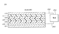
101…基板
103…アノード
105…正孔注入層
107…正孔輸送層
109…発光層
111…電子輸送層
113…カソード
250…電源
260…電気導体
Claims (1)
- 有機発光ダイオード(OLED)表示装置であって、
a)2以上のグループに分割された複数の発光要素であって時間と共に又は使用により変化する出力を有するもの;
b)該表示装置が使用した総電流量を検出して電流信号を発生させるための電流測定デバイス;及び
c)あるグループ内の発光要素の全部を同時に活性化させて、該電流信号に応じ、該グループ内の発光要素について補正信号を計算し、そして該補正信号を入力画像信号に適用することにより該グループ内の発光要素の出力変化を補償する補正入力画像信号を発生させるためのコントローラー
を含んでなるOLED表示装置。
Applications Claiming Priority (1)
| Application Number | Priority Date | Filing Date | Title |
|---|---|---|---|
| US10/355,922 US7161566B2 (en) | 2003-01-31 | 2003-01-31 | OLED display with aging compensation |
Related Child Applications (1)
| Application Number | Title | Priority Date | Filing Date |
|---|---|---|---|
| JP2011192282A Division JP2012027481A (ja) | 2003-01-31 | 2011-09-05 | 有機発光ダイオード(oled)表示装置 |
Publications (1)
| Publication Number | Publication Date |
|---|---|
| JP2004234011A true JP2004234011A (ja) | 2004-08-19 |
Family
ID=32655591
Family Applications (2)
| Application Number | Title | Priority Date | Filing Date |
|---|---|---|---|
| JP2004023121A Withdrawn JP2004234011A (ja) | 2003-01-31 | 2004-01-30 | 有機発光ダイオード(oled)表示装置 |
| JP2011192282A Pending JP2012027481A (ja) | 2003-01-31 | 2011-09-05 | 有機発光ダイオード(oled)表示装置 |
Family Applications After (1)
| Application Number | Title | Priority Date | Filing Date |
|---|---|---|---|
| JP2011192282A Pending JP2012027481A (ja) | 2003-01-31 | 2011-09-05 | 有機発光ダイオード(oled)表示装置 |
Country Status (6)
| Country | Link |
|---|---|
| US (1) | US7161566B2 (ja) |
| EP (1) | EP1443484A3 (ja) |
| JP (2) | JP2004234011A (ja) |
| KR (1) | KR20040070106A (ja) |
| CN (1) | CN100483497C (ja) |
| TW (1) | TWI350123B (ja) |
Cited By (6)
| Publication number | Priority date | Publication date | Assignee | Title |
|---|---|---|---|---|
| JP2006289721A (ja) * | 2005-04-08 | 2006-10-26 | Fuji Photo Film Co Ltd | 光走査装置における光量偏差補正方法 |
| JP2007101697A (ja) * | 2005-09-30 | 2007-04-19 | Fujifilm Corp | 露光装置 |
| JP2007156044A (ja) * | 2005-12-05 | 2007-06-21 | Sony Corp | 自発光表示装置、階調値/劣化率変換テーブル更新装置及びプログラム |
| JP2007206463A (ja) * | 2006-02-02 | 2007-08-16 | Sony Corp | 自発光表示装置、入力表示データ補正装置及びプログラム |
| JP2007206464A (ja) * | 2006-02-02 | 2007-08-16 | Sony Corp | 自発光表示装置、見積もり劣化情報修正装置、入力表示データ補正装置及びプログラム |
| CN102768816A (zh) * | 2012-07-30 | 2012-11-07 | 西安诺瓦电子科技有限公司 | Led显示屏自动化校正方法 |
Families Citing this family (127)
| Publication number | Priority date | Publication date | Assignee | Title |
|---|---|---|---|---|
| US8111222B2 (en) * | 2002-11-21 | 2012-02-07 | Koninklijke Philips Electronics N.V. | Method of improving the output uniformity of a display device |
| CA2419704A1 (en) | 2003-02-24 | 2004-08-24 | Ignis Innovation Inc. | Method of manufacturing a pixel with organic light-emitting diode |
| JP4808913B2 (ja) * | 2003-04-08 | 2011-11-02 | グローバル・オーエルイーディー・テクノロジー・リミテッド・ライアビリティ・カンパニー | 表示装置 |
| US7262753B2 (en) * | 2003-08-07 | 2007-08-28 | Barco N.V. | Method and system for measuring and controlling an OLED display element for improved lifetime and light output |
| CA2443206A1 (en) | 2003-09-23 | 2005-03-23 | Ignis Innovation Inc. | Amoled display backplanes - pixel driver circuits, array architecture, and external compensation |
| US6870323B1 (en) * | 2003-10-02 | 2005-03-22 | Eastman Kodak Company | Color display with white light emitting elements |
| JP2005128089A (ja) * | 2003-10-21 | 2005-05-19 | Tohoku Pioneer Corp | 発光表示装置 |
| US6995519B2 (en) * | 2003-11-25 | 2006-02-07 | Eastman Kodak Company | OLED display with aging compensation |
| GB0328584D0 (en) * | 2003-12-10 | 2004-01-14 | Koninkl Philips Electronics Nv | Video data signal correction |
| EP1548573A1 (en) * | 2003-12-23 | 2005-06-29 | Barco N.V. | Hierarchical control system for a tiled large-screen emissive display |
| US8025831B2 (en) * | 2004-05-24 | 2011-09-27 | Agency For Science, Technology And Research | Imprinting of supported and free-standing 3-D micro- or nano-structures |
| US7274346B2 (en) * | 2004-06-01 | 2007-09-25 | Eastman Kodak Company | Uniformity and brightness measurement in OLED displays |
| US7132805B2 (en) * | 2004-08-09 | 2006-11-07 | Dialight Corporation | Intelligent drive circuit for a light emitting diode (LED) light engine |
| US20060061292A1 (en) * | 2004-09-17 | 2006-03-23 | Samsung Electronics Co., Ltd. | Display device and driving method thereof |
| US7211452B2 (en) * | 2004-09-22 | 2007-05-01 | Eastman Kodak Company | Method and apparatus for uniformity and brightness correction in an OLED display |
| US7812800B2 (en) * | 2004-09-22 | 2010-10-12 | Tpo Displays Corp. | Design Approach and panel and electronic device utilizing the same |
| WO2006037363A1 (de) * | 2004-10-06 | 2006-04-13 | Fraunhofer-Gesellschaft zur Förderung der angewandten Forschung e.V. | Vorrichtung und verfahren zum ansteuern einer organischen leuchtdiode |
| US20060077135A1 (en) * | 2004-10-08 | 2006-04-13 | Eastman Kodak Company | Method for compensating an OLED device for aging |
| US7400345B2 (en) * | 2004-10-22 | 2008-07-15 | Eastman Kodak Company | OLED display with aspect ratio compensation |
| US20060125734A1 (en) | 2004-12-09 | 2006-06-15 | Eastman Kodak Company | OLED display with aging compensation |
| US10013907B2 (en) | 2004-12-15 | 2018-07-03 | Ignis Innovation Inc. | Method and system for programming, calibrating and/or compensating, and driving an LED display |
| US10012678B2 (en) | 2004-12-15 | 2018-07-03 | Ignis Innovation Inc. | Method and system for programming, calibrating and/or compensating, and driving an LED display |
| TWI402790B (zh) | 2004-12-15 | 2013-07-21 | Ignis Innovation Inc | 用以程式化,校準及驅動一發光元件顯示器的方法及系統 |
| US9799246B2 (en) | 2011-05-20 | 2017-10-24 | Ignis Innovation Inc. | System and methods for extraction of threshold and mobility parameters in AMOLED displays |
| US8576217B2 (en) | 2011-05-20 | 2013-11-05 | Ignis Innovation Inc. | System and methods for extraction of threshold and mobility parameters in AMOLED displays |
| US7158106B2 (en) * | 2005-01-12 | 2007-01-02 | Eastman Kodak Company | Temperature measurement using an OLED device |
| CA2495726A1 (en) | 2005-01-28 | 2006-07-28 | Ignis Innovation Inc. | Locally referenced voltage programmed pixel for amoled displays |
| KR100696107B1 (ko) * | 2005-04-11 | 2007-03-19 | 삼성전자주식회사 | 디스플레이장치 및 그 제어방법 |
| FR2886497A1 (fr) * | 2005-05-24 | 2006-12-01 | Thomson Licensing Sa | Dispositif d'affichage d'images video a matrice active avec correction des non-uniformites de luminance |
| CN102663977B (zh) | 2005-06-08 | 2015-11-18 | 伊格尼斯创新有限公司 | 用于驱动发光器件显示器的方法和系统 |
| TWI309028B (en) * | 2005-06-13 | 2009-04-21 | Novatek Microelectronics Corp | Method for calibrating a flat panel display |
| US9318053B2 (en) * | 2005-07-04 | 2016-04-19 | Semiconductor Energy Laboratory Co., Ltd. | Semiconductor device and driving method thereof |
| US7391335B2 (en) * | 2005-08-18 | 2008-06-24 | Honeywell International, Inc. | Aerospace light-emitting diode (LED)-based lights life and operation monitor compensator |
| DE102005042704A1 (de) * | 2005-09-01 | 2007-03-08 | Ingenieurbüro Kienhöfer GmbH | Verfahren zum Betreiben einer Anzeigevorrichtung mit einer Mehrzahl von verschleißbehafteten Bildelementen und Anzeigevorrichtung |
| KR101333025B1 (ko) * | 2005-09-29 | 2013-11-26 | 코닌클리케 필립스 엔.브이. | 조명 디바이스의 노화 프로세스를 보상하는 방법 및 그조명 디바이스 |
| EP1784055A3 (en) * | 2005-10-17 | 2009-08-05 | Semiconductor Energy Laboratory Co., Ltd. | Lighting system |
| US8558765B2 (en) * | 2005-11-07 | 2013-10-15 | Global Oled Technology Llc | Method and apparatus for uniformity and brightness correction in an electroluminescent display |
| US8207914B2 (en) * | 2005-11-07 | 2012-06-26 | Global Oled Technology Llc | OLED display with aging compensation |
| US20080055209A1 (en) * | 2006-08-30 | 2008-03-06 | Eastman Kodak Company | Method and apparatus for uniformity and brightness correction in an amoled display |
| US7505949B2 (en) * | 2006-01-31 | 2009-03-17 | Caterpillar Inc. | Process model error correction method and system |
| US20080048951A1 (en) * | 2006-04-13 | 2008-02-28 | Naugler Walter E Jr | Method and apparatus for managing and uniformly maintaining pixel circuitry in a flat panel display |
| CN101501748B (zh) | 2006-04-19 | 2012-12-05 | 伊格尼斯创新有限公司 | 有源矩阵显示器的稳定驱动设计 |
| US20070268414A1 (en) * | 2006-05-21 | 2007-11-22 | Ming-Tso Hsu | Method and system for distributing pvr functionalities |
| US20070290947A1 (en) * | 2006-06-16 | 2007-12-20 | Cok Ronald S | Method and apparatus for compensating aging of an electroluminescent display |
| US7696965B2 (en) * | 2006-06-16 | 2010-04-13 | Global Oled Technology Llc | Method and apparatus for compensating aging of OLED display |
| US20080042943A1 (en) * | 2006-06-16 | 2008-02-21 | Cok Ronald S | Method and apparatus for averaged luminance and uniformity correction in an am-el display |
| US8176319B2 (en) * | 2006-06-27 | 2012-05-08 | Emc Corporation | Identifying and enforcing strict file confidentiality in the presence of system and storage administrators in a NAS system |
| KR20080010796A (ko) * | 2006-07-28 | 2008-01-31 | 삼성전자주식회사 | 유기 발광 표시 장치 및 그의 구동 방법 |
| CA2556961A1 (en) | 2006-08-15 | 2008-02-15 | Ignis Innovation Inc. | Oled compensation technique based on oled capacitance |
| GB2441354B (en) * | 2006-08-31 | 2009-07-29 | Cambridge Display Tech Ltd | Display drive systems |
| KR100787221B1 (ko) * | 2006-09-26 | 2007-12-21 | 삼성전자주식회사 | Led 기반 광시스템 및 그의 노화 보상방법 |
| TW200818973A (en) * | 2006-10-11 | 2008-04-16 | Au Optronics Corp | Temperature regulative display system and controlling method of amoled panel |
| US20080122759A1 (en) * | 2006-11-28 | 2008-05-29 | Levey Charles I | Active matrix display compensating method |
| KR101310376B1 (ko) * | 2006-12-20 | 2013-09-23 | 엘지디스플레이 주식회사 | 유기 발광다이오드 표시장치와 그 구동방법 |
| US7847764B2 (en) * | 2007-03-15 | 2010-12-07 | Global Oled Technology Llc | LED device compensation method |
| CN101295465B (zh) * | 2007-04-27 | 2010-12-22 | 深圳市同洲电子股份有限公司 | Led衰老校正方法及装置 |
| DE102007040079A1 (de) * | 2007-08-24 | 2009-02-26 | Ledon Lighting Gmbh | Verfahren zur Bestimmung des Lichtstroms einer Lichtquelle |
| US8405585B2 (en) * | 2008-01-04 | 2013-03-26 | Chimei Innolux Corporation | OLED display, information device, and method for displaying an image in OLED display |
| FI122051B (fi) * | 2008-06-27 | 2011-07-29 | Valopaa Oy | Valaisin ja ohjausmenetelmä |
| US20100201275A1 (en) | 2009-02-06 | 2010-08-12 | Cok Ronald S | Light sensing in display device |
| US8350495B2 (en) | 2009-06-05 | 2013-01-08 | Light-Based Technologies Incorporated | Device driver providing compensation for aging |
| US9311859B2 (en) | 2009-11-30 | 2016-04-12 | Ignis Innovation Inc. | Resetting cycle for aging compensation in AMOLED displays |
| CA2669367A1 (en) | 2009-06-16 | 2010-12-16 | Ignis Innovation Inc | Compensation technique for color shift in displays |
| US9384698B2 (en) | 2009-11-30 | 2016-07-05 | Ignis Innovation Inc. | System and methods for aging compensation in AMOLED displays |
| US10319307B2 (en) | 2009-06-16 | 2019-06-11 | Ignis Innovation Inc. | Display system with compensation techniques and/or shared level resources |
| US8633873B2 (en) | 2009-11-12 | 2014-01-21 | Ignis Innovation Inc. | Stable fast programming scheme for displays |
| CA2692097A1 (en) | 2010-02-04 | 2011-08-04 | Ignis Innovation Inc. | Extracting correlation curves for light emitting device |
| US10089921B2 (en) | 2010-02-04 | 2018-10-02 | Ignis Innovation Inc. | System and methods for extracting correlation curves for an organic light emitting device |
| US20140313111A1 (en) | 2010-02-04 | 2014-10-23 | Ignis Innovation Inc. | System and methods for extracting correlation curves for an organic light emitting device |
| US9881532B2 (en) | 2010-02-04 | 2018-01-30 | Ignis Innovation Inc. | System and method for extracting correlation curves for an organic light emitting device |
| US8711099B2 (en) | 2010-05-10 | 2014-04-29 | Blackberry Limited | Handheld electronic communication device having sliding display |
| JP2012073400A (ja) * | 2010-09-28 | 2012-04-12 | Sanyo Electric Co Ltd | 表示装置 |
| US8907991B2 (en) | 2010-12-02 | 2014-12-09 | Ignis Innovation Inc. | System and methods for thermal compensation in AMOLED displays |
| US8723890B2 (en) | 2010-12-23 | 2014-05-13 | Blackberry Limited | Handheld electronic device having sliding display and position configurable camera |
| US8514179B2 (en) | 2010-12-23 | 2013-08-20 | Research In Motion Limited | Handheld electronic communication device having an age compensating display |
| US9606607B2 (en) | 2011-05-17 | 2017-03-28 | Ignis Innovation Inc. | Systems and methods for display systems with dynamic power control |
| US9530349B2 (en) | 2011-05-20 | 2016-12-27 | Ignis Innovations Inc. | Charged-based compensation and parameter extraction in AMOLED displays |
| US9466240B2 (en) | 2011-05-26 | 2016-10-11 | Ignis Innovation Inc. | Adaptive feedback system for compensating for aging pixel areas with enhanced estimation speed |
| US9773439B2 (en) | 2011-05-27 | 2017-09-26 | Ignis Innovation Inc. | Systems and methods for aging compensation in AMOLED displays |
| US8901579B2 (en) | 2011-08-03 | 2014-12-02 | Ignis Innovation Inc. | Organic light emitting diode and method of manufacturing |
| US10089924B2 (en) | 2011-11-29 | 2018-10-02 | Ignis Innovation Inc. | Structural and low-frequency non-uniformity compensation |
| US9385169B2 (en) | 2011-11-29 | 2016-07-05 | Ignis Innovation Inc. | Multi-functional active matrix organic light-emitting diode display |
| US9324268B2 (en) | 2013-03-15 | 2016-04-26 | Ignis Innovation Inc. | Amoled displays with multiple readout circuits |
| KR101228885B1 (ko) * | 2011-12-21 | 2013-02-01 | 엘지디스플레이 주식회사 | 유기발광표시장치 및 그 제조방법 |
| US8937632B2 (en) | 2012-02-03 | 2015-01-20 | Ignis Innovation Inc. | Driving system for active-matrix displays |
| US8922544B2 (en) | 2012-05-23 | 2014-12-30 | Ignis Innovation Inc. | Display systems with compensation for line propagation delay |
| US8922599B2 (en) | 2012-08-23 | 2014-12-30 | Blackberry Limited | Organic light emitting diode based display aging monitoring |
| KR101962897B1 (ko) | 2012-08-30 | 2019-03-29 | 삼성디스플레이 주식회사 | 화소 및 이를 이용한 유기전계발광 표시장치 |
| US9721505B2 (en) | 2013-03-08 | 2017-08-01 | Ignis Innovation Inc. | Pixel circuits for AMOLED displays |
| EP3043338A1 (en) | 2013-03-14 | 2016-07-13 | Ignis Innovation Inc. | Re-interpolation with edge detection for extracting an aging pattern for amoled displays |
| WO2014140992A1 (en) | 2013-03-15 | 2014-09-18 | Ignis Innovation Inc. | Dynamic adjustment of touch resolutions on an amoled display |
| US9741282B2 (en) | 2013-12-06 | 2017-08-22 | Ignis Innovation Inc. | OLED display system and method |
| US9761170B2 (en) | 2013-12-06 | 2017-09-12 | Ignis Innovation Inc. | Correction for localized phenomena in an image array |
| US9059337B1 (en) * | 2013-12-24 | 2015-06-16 | Christie Digital Systems Usa, Inc. | Method, system and apparatus for dynamically monitoring and calibrating display tiles |
| US9502653B2 (en) | 2013-12-25 | 2016-11-22 | Ignis Innovation Inc. | Electrode contacts |
| US10997901B2 (en) | 2014-02-28 | 2021-05-04 | Ignis Innovation Inc. | Display system |
| US10176752B2 (en) | 2014-03-24 | 2019-01-08 | Ignis Innovation Inc. | Integrated gate driver |
| DE102015206281A1 (de) | 2014-04-08 | 2015-10-08 | Ignis Innovation Inc. | Anzeigesystem mit gemeinsam genutzten Niveauressourcen für tragbare Vorrichtungen |
| CN103927989B (zh) * | 2014-04-21 | 2016-09-21 | 中国电子科技集团公司第五十五研究所 | 具有宽温亮度补偿功能的无源有机发光二极管显示装置及亮度补偿方法 |
| CN109346005B (zh) * | 2014-06-26 | 2021-10-01 | 萤光勒克斯株式会社 | 有机el面板控制装置、光源装置、有机el面板控制方法、程序以及记录介质 |
| CN104361859B (zh) * | 2014-11-18 | 2017-01-11 | 深圳市华星光电技术有限公司 | 显示装置及其亮度调节方法 |
| CA2872563A1 (en) | 2014-11-28 | 2016-05-28 | Ignis Innovation Inc. | High pixel density array architecture |
| TWI540566B (zh) * | 2014-12-09 | 2016-07-01 | 緯創資通股份有限公司 | 顯示器及其亮度、色彩補償方法與系統 |
| CA2879462A1 (en) | 2015-01-23 | 2016-07-23 | Ignis Innovation Inc. | Compensation for color variation in emissive devices |
| CA2889870A1 (en) | 2015-05-04 | 2016-11-04 | Ignis Innovation Inc. | Optical feedback system |
| CA2892714A1 (en) | 2015-05-27 | 2016-11-27 | Ignis Innovation Inc | Memory bandwidth reduction in compensation system |
| US10373554B2 (en) | 2015-07-24 | 2019-08-06 | Ignis Innovation Inc. | Pixels and reference circuits and timing techniques |
| CA2898282A1 (en) | 2015-07-24 | 2017-01-24 | Ignis Innovation Inc. | Hybrid calibration of current sources for current biased voltage progra mmed (cbvp) displays |
| US10657895B2 (en) | 2015-07-24 | 2020-05-19 | Ignis Innovation Inc. | Pixels and reference circuits and timing techniques |
| KR102435923B1 (ko) * | 2015-08-05 | 2022-08-25 | 삼성디스플레이 주식회사 | 유기 발광 표시 장치 및 이의 구동 방법 |
| CA2900170A1 (en) | 2015-08-07 | 2017-02-07 | Gholamreza Chaji | Calibration of pixel based on improved reference values |
| CA2909813A1 (en) | 2015-10-26 | 2017-04-26 | Ignis Innovation Inc | High ppi pattern orientation |
| CN105825797B (zh) * | 2016-03-31 | 2020-01-14 | Oppo广东移动通信有限公司 | 一种显示屏的检测方法、检测装置以及终端 |
| CN105895056B (zh) | 2016-06-17 | 2017-04-19 | 京东方科技集团股份有限公司 | 亮度补偿模型的建立方法、屏幕亮度的补偿方法及装置 |
| CN106093529B (zh) | 2016-07-19 | 2019-03-12 | 京东方科技集团股份有限公司 | 电流测量校准方法、电流测量方法及装置、显示装置 |
| US10586491B2 (en) | 2016-12-06 | 2020-03-10 | Ignis Innovation Inc. | Pixel circuits for mitigation of hysteresis |
| US10714018B2 (en) | 2017-05-17 | 2020-07-14 | Ignis Innovation Inc. | System and method for loading image correction data for displays |
| KR102326166B1 (ko) * | 2017-06-30 | 2021-11-16 | 엘지디스플레이 주식회사 | 전계 발광 표시장치와 그 구동방법 |
| CN109307587B (zh) * | 2017-07-26 | 2020-01-31 | 京东方科技集团股份有限公司 | 显示面板检测方法、装置及系统 |
| US11025899B2 (en) | 2017-08-11 | 2021-06-01 | Ignis Innovation Inc. | Optical correction systems and methods for correcting non-uniformity of emissive display devices |
| KR102644412B1 (ko) * | 2017-11-16 | 2024-03-06 | 시냅틱스 인코포레이티드 | 디스플레이 패널을 위한 보상 기술 |
| US10971078B2 (en) | 2018-02-12 | 2021-04-06 | Ignis Innovation Inc. | Pixel measurement through data line |
| KR20190100577A (ko) * | 2018-02-21 | 2019-08-29 | 삼성전자주식회사 | 픽셀의 열화량을 산출하는 전자 장치 |
| KR102033460B1 (ko) * | 2018-04-30 | 2019-10-17 | 배재대학교 산학협력단 | Oled 에이징 시스템 및 방법 |
| JP2021071680A (ja) * | 2019-11-01 | 2021-05-06 | セイコーエプソン株式会社 | 表示装置、頭部装着型表示装置および表示方法 |
| TWI809997B (zh) * | 2022-07-28 | 2023-07-21 | 大陸商北京集創北方科技股份有限公司 | Led顯示驅動的色溫補償方法、led顯示驅動晶片及led顯示裝置 |
| TWI845226B (zh) * | 2023-03-24 | 2024-06-11 | 友達光電股份有限公司 | 亮度補償裝置及亮度補償方法 |
Citations (7)
| Publication number | Priority date | Publication date | Assignee | Title |
|---|---|---|---|---|
| JPH09305145A (ja) * | 1996-05-16 | 1997-11-28 | Fuji Electric Co Ltd | 表示素子駆動方法 |
| JPH11219146A (ja) * | 1997-09-29 | 1999-08-10 | Mitsubishi Chemical Corp | アクティブマトリックス発光ダイオード画素構造およびその方法 |
| JP2000056732A (ja) * | 1998-08-12 | 2000-02-25 | Tdk Corp | 有機el表示装置 |
| JP2002215094A (ja) * | 2001-01-16 | 2002-07-31 | Sony Corp | 画像表示装置とその駆動方法 |
| JP2003122305A (ja) * | 2001-10-10 | 2003-04-25 | Sony Corp | 有機el表示装置およびその制御方法 |
| JP2003195816A (ja) * | 2001-12-26 | 2003-07-09 | Sony Corp | 有機el表示装置およびその制御方法 |
| JP2003330418A (ja) * | 2002-05-14 | 2003-11-19 | Sony Corp | 表示装置およびその駆動方法 |
Family Cites Families (16)
| Publication number | Priority date | Publication date | Assignee | Title |
|---|---|---|---|---|
| DE69825402T2 (de) | 1997-03-12 | 2005-08-04 | Seiko Epson Corp. | Pixelschaltung, anzeigevorrichtung und elektronische apparatur mit stromgesteuerter lichtemittierender vorrichtung |
| US6504565B1 (en) | 1998-09-21 | 2003-01-07 | Canon Kabushiki Kaisha | Light-emitting device, exposure device, and image forming apparatus |
| EP1079361A1 (en) * | 1999-08-20 | 2001-02-28 | Harness System Technologies Research, Ltd. | Driver for electroluminescent elements |
| CN1377495A (zh) * | 1999-10-04 | 2002-10-30 | 松下电器产业株式会社 | 显示面板的驱动方法、显示面板的亮度校正装置及其驱动装置 |
| WO2001027910A1 (en) * | 1999-10-12 | 2001-04-19 | Koninklijke Philips Electronics N.V. | Led display device |
| US6414661B1 (en) | 2000-02-22 | 2002-07-02 | Sarnoff Corporation | Method and apparatus for calibrating display devices and automatically compensating for loss in their efficiency over time |
| EP1158483A3 (en) * | 2000-05-24 | 2003-02-05 | Eastman Kodak Company | Solid-state display with reference pixel |
| US20020030647A1 (en) * | 2000-06-06 | 2002-03-14 | Michael Hack | Uniform active matrix oled displays |
| SG107573A1 (en) * | 2001-01-29 | 2004-12-29 | Semiconductor Energy Lab | Light emitting device |
| SG111928A1 (en) * | 2001-01-29 | 2005-06-29 | Semiconductor Energy Lab | Light emitting device |
| TWI248319B (en) * | 2001-02-08 | 2006-01-21 | Semiconductor Energy Lab | Light emitting device and electronic equipment using the same |
| JP2002278514A (ja) | 2001-03-19 | 2002-09-27 | Sharp Corp | 電気光学装置 |
| US6963321B2 (en) | 2001-05-09 | 2005-11-08 | Clare Micronix Integrated Systems, Inc. | Method of providing pulse amplitude modulation for OLED display drivers |
| US6944424B2 (en) * | 2001-07-23 | 2005-09-13 | Intermec Ip Corp. | RFID tag having combined battery and passive power source |
| US6456016B1 (en) | 2001-07-30 | 2002-09-24 | Intel Corporation | Compensating organic light emitting device displays |
| SG120888A1 (en) * | 2001-09-28 | 2006-04-26 | Semiconductor Energy Lab | A light emitting device and electronic apparatus using the same |
-
2003
- 2003-01-31 US US10/355,922 patent/US7161566B2/en not_active Expired - Lifetime
- 2003-12-09 TW TW092134692A patent/TWI350123B/zh not_active IP Right Cessation
-
2004
- 2004-01-19 EP EP04075154A patent/EP1443484A3/en not_active Withdrawn
- 2004-01-30 JP JP2004023121A patent/JP2004234011A/ja not_active Withdrawn
- 2004-01-31 KR KR1020040006474A patent/KR20040070106A/ko not_active Ceased
- 2004-01-31 CN CNB2004100038467A patent/CN100483497C/zh not_active Expired - Lifetime
-
2011
- 2011-09-05 JP JP2011192282A patent/JP2012027481A/ja active Pending
Patent Citations (7)
| Publication number | Priority date | Publication date | Assignee | Title |
|---|---|---|---|---|
| JPH09305145A (ja) * | 1996-05-16 | 1997-11-28 | Fuji Electric Co Ltd | 表示素子駆動方法 |
| JPH11219146A (ja) * | 1997-09-29 | 1999-08-10 | Mitsubishi Chemical Corp | アクティブマトリックス発光ダイオード画素構造およびその方法 |
| JP2000056732A (ja) * | 1998-08-12 | 2000-02-25 | Tdk Corp | 有機el表示装置 |
| JP2002215094A (ja) * | 2001-01-16 | 2002-07-31 | Sony Corp | 画像表示装置とその駆動方法 |
| JP2003122305A (ja) * | 2001-10-10 | 2003-04-25 | Sony Corp | 有機el表示装置およびその制御方法 |
| JP2003195816A (ja) * | 2001-12-26 | 2003-07-09 | Sony Corp | 有機el表示装置およびその制御方法 |
| JP2003330418A (ja) * | 2002-05-14 | 2003-11-19 | Sony Corp | 表示装置およびその駆動方法 |
Cited By (6)
| Publication number | Priority date | Publication date | Assignee | Title |
|---|---|---|---|---|
| JP2006289721A (ja) * | 2005-04-08 | 2006-10-26 | Fuji Photo Film Co Ltd | 光走査装置における光量偏差補正方法 |
| JP2007101697A (ja) * | 2005-09-30 | 2007-04-19 | Fujifilm Corp | 露光装置 |
| JP2007156044A (ja) * | 2005-12-05 | 2007-06-21 | Sony Corp | 自発光表示装置、階調値/劣化率変換テーブル更新装置及びプログラム |
| JP2007206463A (ja) * | 2006-02-02 | 2007-08-16 | Sony Corp | 自発光表示装置、入力表示データ補正装置及びプログラム |
| JP2007206464A (ja) * | 2006-02-02 | 2007-08-16 | Sony Corp | 自発光表示装置、見積もり劣化情報修正装置、入力表示データ補正装置及びプログラム |
| CN102768816A (zh) * | 2012-07-30 | 2012-11-07 | 西安诺瓦电子科技有限公司 | Led显示屏自动化校正方法 |
Also Published As
| Publication number | Publication date |
|---|---|
| CN1519796A (zh) | 2004-08-11 |
| EP1443484A2 (en) | 2004-08-04 |
| JP2012027481A (ja) | 2012-02-09 |
| US7161566B2 (en) | 2007-01-09 |
| KR20040070106A (ko) | 2004-08-06 |
| TWI350123B (en) | 2011-10-01 |
| CN100483497C (zh) | 2009-04-29 |
| US20040150590A1 (en) | 2004-08-05 |
| EP1443484A3 (en) | 2010-02-17 |
| TW200414807A (en) | 2004-08-01 |
Similar Documents
| Publication | Publication Date | Title |
|---|---|---|
| JP2004234011A (ja) | 有機発光ダイオード(oled)表示装置 | |
| CN1886774B (zh) | 具有老化补偿的oled显示器 | |
| CN101595519B (zh) | 具有老化和效率补偿的oled显示器 | |
| US8207914B2 (en) | OLED display with aging compensation | |
| JP5209709B2 (ja) | Oled駆動回路の特性変化の補償方法 | |
| KR100995825B1 (ko) | 광센서를 갖는 유기발광다이오드 디스플레이 | |
| US7977877B2 (en) | Flat panel OLED device having deformable substrate | |
| US7973473B2 (en) | Flat panel OLED device having deformable substrate |
Legal Events
| Date | Code | Title | Description |
|---|---|---|---|
| A621 | Written request for application examination |
Free format text: JAPANESE INTERMEDIATE CODE: A621 Effective date: 20070117 |
|
| A131 | Notification of reasons for refusal |
Free format text: JAPANESE INTERMEDIATE CODE: A131 Effective date: 20100119 |
|
| A601 | Written request for extension of time |
Free format text: JAPANESE INTERMEDIATE CODE: A601 Effective date: 20100324 |
|
| A602 | Written permission of extension of time |
Free format text: JAPANESE INTERMEDIATE CODE: A602 Effective date: 20100329 |
|
| A521 | Request for written amendment filed |
Free format text: JAPANESE INTERMEDIATE CODE: A523 Effective date: 20100716 |
|
| A711 | Notification of change in applicant |
Free format text: JAPANESE INTERMEDIATE CODE: A711 Effective date: 20100803 |
|
| A02 | Decision of refusal |
Free format text: JAPANESE INTERMEDIATE CODE: A02 Effective date: 20110510 |
|
| A521 | Request for written amendment filed |
Free format text: JAPANESE INTERMEDIATE CODE: A523 Effective date: 20110905 |
|
| A911 | Transfer to examiner for re-examination before appeal (zenchi) |
Free format text: JAPANESE INTERMEDIATE CODE: A911 Effective date: 20110913 |
|
| A761 | Written withdrawal of application |
Free format text: JAPANESE INTERMEDIATE CODE: A761 Effective date: 20110922 |