JP2004234822A - Soiセンス・アンプ - Google Patents
Soiセンス・アンプ Download PDFInfo
- Publication number
- JP2004234822A JP2004234822A JP2004001470A JP2004001470A JP2004234822A JP 2004234822 A JP2004234822 A JP 2004234822A JP 2004001470 A JP2004001470 A JP 2004001470A JP 2004001470 A JP2004001470 A JP 2004001470A JP 2004234822 A JP2004234822 A JP 2004234822A
- Authority
- JP
- Japan
- Prior art keywords
- fet
- sense amplifier
- input
- source
- latch
- Prior art date
- Legal status (The legal status is an assumption and is not a legal conclusion. Google has not performed a legal analysis and makes no representation as to the accuracy of the status listed.)
- Granted
Links
- 238000005516 engineering process Methods 0.000 claims abstract description 16
- 238000000034 method Methods 0.000 claims abstract description 12
- 230000035945 sensitivity Effects 0.000 claims abstract description 4
- 238000004519 manufacturing process Methods 0.000 claims description 2
- 230000001960 triggered effect Effects 0.000 claims description 2
- 230000000694 effects Effects 0.000 abstract description 3
- 238000010586 diagram Methods 0.000 description 5
- 238000013459 approach Methods 0.000 description 4
- 230000000295 complement effect Effects 0.000 description 3
- 230000005669 field effect Effects 0.000 description 2
- 230000003321 amplification Effects 0.000 description 1
- 238000004458 analytical method Methods 0.000 description 1
- 230000001934 delay Effects 0.000 description 1
- 230000001419 dependent effect Effects 0.000 description 1
- 238000001514 detection method Methods 0.000 description 1
- 230000001627 detrimental effect Effects 0.000 description 1
- 230000005611 electricity Effects 0.000 description 1
- 239000012212 insulator Substances 0.000 description 1
- WABPQHHGFIMREM-UHFFFAOYSA-N lead(0) Chemical compound [Pb] WABPQHHGFIMREM-UHFFFAOYSA-N 0.000 description 1
- 238000003199 nucleic acid amplification method Methods 0.000 description 1
- 230000035484 reaction time Effects 0.000 description 1
- 230000004044 response Effects 0.000 description 1
- 229910052710 silicon Inorganic materials 0.000 description 1
- 239000010703 silicon Substances 0.000 description 1
- 230000003068 static effect Effects 0.000 description 1
- 230000001360 synchronised effect Effects 0.000 description 1
Images



Classifications
-
- H—ELECTRICITY
- H03—ELECTRONIC CIRCUITRY
- H03K—PULSE TECHNIQUE
- H03K3/00—Circuits for generating electric pulses; Monostable, bistable or multistable circuits
- H03K3/02—Generators characterised by the type of circuit or by the means used for producing pulses
- H03K3/353—Generators characterised by the type of circuit or by the means used for producing pulses by the use, as active elements, of field-effect transistors with internal or external positive feedback
- H03K3/356—Bistable circuits
- H03K3/356104—Bistable circuits using complementary field-effect transistors
- H03K3/356113—Bistable circuits using complementary field-effect transistors using additional transistors in the input circuit
- H03K3/35613—Bistable circuits using complementary field-effect transistors using additional transistors in the input circuit the input circuit having a differential configuration
- H03K3/356139—Bistable circuits using complementary field-effect transistors using additional transistors in the input circuit the input circuit having a differential configuration with synchronous operation
-
- G—PHYSICS
- G11—INFORMATION STORAGE
- G11C—STATIC STORES
- G11C7/00—Arrangements for writing information into, or reading information out from, a digital store
- G11C7/06—Sense amplifiers; Associated circuits, e.g. timing or triggering circuits
- G11C7/065—Differential amplifiers of latching type
-
- H—ELECTRICITY
- H03—ELECTRONIC CIRCUITRY
- H03K—PULSE TECHNIQUE
- H03K3/00—Circuits for generating electric pulses; Monostable, bistable or multistable circuits
- H03K3/01—Details
- H03K3/011—Modifications of generator to compensate for variations in physical values, e.g. voltage, temperature
Landscapes
- Static Random-Access Memory (AREA)
- Dram (AREA)
Abstract
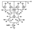
【解決手段】 クロス結合ラッチは、ボディがソースおよびドレインのうちの一方に接続されたボディ・コンタクトFET84,86を有し、スイッチング履歴効果を最小化し、入力FET80,82が通常のゲート・スイッチング電圧より高いゲート・スイッチング電圧を有すると同時に、入力信号感度を増加させる。
【選択図】図4
Description
(1)SOIシステムにおいて用いられるセンス・アンプであって、ラッチ・ノードを構成するボディ/ソース構成の一対のクロス結合並列インバータであって、それぞれがサイクルの異なる部分においてトリガされる一対のクロス結合並列インバータと、一対の高スレショルド電圧NFET並列入力デバイスであって、それぞれが前記インバータのうちのそれぞれ異なる一方と相互接続される一対の高スレショルド電圧NFET並列入力デバイスと、を備えるセンス・アンプ。
(2)一対のFETラッチであって、それぞれのラッチが、ボディがソースおよびドレインのうちの一方と接続される少なくとも1つのFETを含む一対のFETラッチと、一対の高スレショルド電圧FET並列入力デバイスであって、それぞれが前記FETラッチのうちのそれぞれ異なる一方と相互接続される一対の高スレショルド電圧FET並列入力デバイスと、を備えるセンス・アンプ。
(3)前記センス・アンプを作成する際に用いられる製造手法はSOIベースであり、接続されたボディを有する前記ラッチ内のFETはNFETであり、前記ボディは前記ソースに接続される上記(2)記載のセンス・アンプ。
(4)前記高スレショルド電圧FET入力デバイスはNFETである上記(2)記載のセンス・アンプ。
(5)SOIテクノロジ・センス・アンプ内の入力デバイスの感度を上げる方法であって、入力FETを作成し、ソース/ゲート電圧であって、前記ソース/ゲート電圧未満で前記入力FETが導通しなくなるソース/ゲート電圧を、前記センス・アンプ内の他のFETと比べて上昇させる工程を含む方法。
(6)一対のFETラッチであって、それぞれのラッチが少なくとも1つのボディ・コンタクト・タイプFETを有する一対のFETラッチと、一対のボディ・コンタクトFET並列信号入力デバイスであって、それぞれが前記FETラッチのそれぞれ異なる一方と相互接続される一対のボディ・コンタクトFET並列信号入力デバイスと、を備えるセンス・アンプ。
(7)前記信号入力デバイスは、前記センス・アンプ内の他のFETより高いスレショルド電圧を有する上記(6)記載のセンス・アンプ。
(8)前記FETラッチのボディ・コンタクトFETは、それぞれ、ソースおよびドレイン端子部を有し、前記FETラッチのボディ・コンタクトFETは、前記ソースおよびドレイン端子部のうちの一方と接続されたボディを有する上記(6)記載のセンス・アンプ。
(9)センス・アンプ内の入力信号履歴によるスイッチング遅延変動を低減させる方法であって、フローティング・ボディ・テクノロジを用いて、前記センス・アンプの2つのラッチ部のそれぞれ内に少なくとも1つのFETを作る工程と、前記少なくとも1つのFETのそれぞれのボディを、ソースおよびドレイン端子の一方へ電気的に接続する工程と、を含む方法。
(10)SOIテクノロジに従って作成された2重ラッチ部および入力信号部を有するセンス・アンプであって、前記入力信号部の一部を含むボディ・コンタクト構成入力信号FETと、前記ラッチ部のそれぞれ内の少なくとも1つのボディ・コンタクト構成FETと、前記ボディ・コンタクト構成FETのそれぞれのボディを、アース,それぞれのFETのソース端子,およびそれぞれのFETのドレイン端子のうちの1つに相互接続する電気的手段と、を備えるセンス・アンプ。
(11)SOIテクノロジに従って作成された2重ラッチ部および入力信号部を有するセンス・アンプであって、前記入力信号部内に含まれた高スレショルド入力信号ボディ・コンタクト構成入力信号FETと、前記ボディ・コンタクト構成FETのそれぞれのボディをアースに相互接続する電気的手段と、を備えるセンス・アンプ。
(12)SOIテクノロジ・センス・アンプの利得を増加させる方法であって、ボディ・コンタクト・デバイスの形態で入力FETを作成する工程と、前記入力FETが高入力信号スレショルドを有するように前記入力FETのパラメータを調整する工程と、前記入力FETのボディをアースに接続する工程と、を含む方法。
20,26,28,30,32 N型FET
22 正電圧
24,34,36,38,40,42 リード線
44 アース
46,48 ゲート
70,72,74,76 接地ボディ・コンタクトFET
80,82 高スレショルド電圧FET
84,86 ボディ・コンタクトFET
Claims (12)
- SOIシステムにおいて用いられるセンス・アンプであって、
ラッチ・ノードを構成するボディ/ソース構成の一対のクロス結合並列インバータであって、それぞれがサイクルの異なる部分においてトリガされる一対のクロス結合並列インバータと、
一対の高スレショルド電圧NFET並列入力デバイスであって、それぞれが前記インバータのうちのそれぞれ異なる一方と相互接続される一対の高スレショルド電圧NFET並列入力デバイスと、を備えるセンス・アンプ。 - 一対のFETラッチであって、それぞれのラッチが、ボディがソースおよびドレインのうちの一方と接続される少なくとも1つのFETを含む一対のFETラッチと、
一対の高スレショルド電圧FET並列入力デバイスであって、それぞれが前記FETラッチのうちのそれぞれ異なる一方と相互接続される一対の高スレショルド電圧FET並列入力デバイスと、を備えるセンス・アンプ。 - 前記センス・アンプを作成する際に用いられる製造手法はSOIベースであり、
接続されたボディを有する前記ラッチ内のFETはNFETであり、前記ボディは前記ソースに接続される請求項2記載のセンス・アンプ。 - 前記高スレショルド電圧FET入力デバイスはNFETである請求項2記載のセンス・アンプ。
- SOIテクノロジ・センス・アンプ内の入力デバイスの感度を上げる方法であって、
入力FETを作成し、ソース/ゲート電圧であって、前記ソース/ゲート電圧未満で前記入力FETが導通しなくなるソース/ゲート電圧を、前記センス・アンプ内の他のFETと比べて上昇させる工程を含む方法。 - 一対のFETラッチであって、それぞれのラッチが少なくとも1つのボディ・コンタクト・タイプFETを有する一対のFETラッチと、
一対のボディ・コンタクトFET並列信号入力デバイスであって、それぞれが前記FETラッチのそれぞれ異なる一方と相互接続される一対のボディ・コンタクトFET並列信号入力デバイスと、を備えるセンス・アンプ。 - 前記信号入力デバイスは、前記センス・アンプ内の他のFETより高いスレショルド電圧を有する請求項6記載のセンス・アンプ。
- 前記FETラッチのボディ・コンタクトFETは、それぞれ、ソースおよびドレイン端子部を有し、
前記FETラッチのボディ・コンタクトFETは、前記ソースおよびドレイン端子部のうちの一方と接続されたボディを有する請求項6記載のセンス・アンプ。 - センス・アンプ内の入力信号履歴によるスイッチング遅延変動を低減させる方法であって、
フローティング・ボディ・テクノロジを用いて、前記センス・アンプの2つのラッチ部のそれぞれ内に少なくとも1つのFETを作る工程と、
前記少なくとも1つのFETのそれぞれのボディを、ソースおよびドレイン端子の一方へ電気的に接続する工程と、を含む方法。 - SOIテクノロジに従って作成された2重ラッチ部および入力信号部を有するセンス・アンプであって、
前記入力信号部の一部を含むボディ・コンタクト構成入力信号FETと、
前記ラッチ部のそれぞれ内の少なくとも1つのボディ・コンタクト構成FETと、
前記ボディ・コンタクト構成FETのそれぞれのボディを、アース,それぞれのFETのソース端子,およびそれぞれのFETのドレイン端子のうちの1つに相互接続する電気的手段と、を備えるセンス・アンプ。 - SOIテクノロジに従って作成された2重ラッチ部および入力信号部を有するセンス・アンプであって、
前記入力信号部内に含まれた高スレショルド入力信号ボディ・コンタクト構成入力信号FETと、
前記ボディ・コンタクト構成FETのそれぞれのボディをアースに相互接続する電気的手段と、を備えるセンス・アンプ。 - SOIテクノロジ・センス・アンプの利得を増加させる方法であって、
ボディ・コンタクト・デバイスの形態で入力FETを作成する工程と、
前記入力FETが高入力信号スレショルドを有するように前記入力FETのパラメータを調整する工程と、
前記入力FETのボディをアースに接続する工程と、を含む方法。
Applications Claiming Priority (1)
| Application Number | Priority Date | Filing Date | Title |
|---|---|---|---|
| US10/355,682 US6833737B2 (en) | 2003-01-30 | 2003-01-30 | SOI sense amplifier method and apparatus |
Publications (2)
| Publication Number | Publication Date |
|---|---|
| JP2004234822A true JP2004234822A (ja) | 2004-08-19 |
| JP4527985B2 JP4527985B2 (ja) | 2010-08-18 |
Family
ID=32770591
Family Applications (1)
| Application Number | Title | Priority Date | Filing Date |
|---|---|---|---|
| JP2004001470A Expired - Fee Related JP4527985B2 (ja) | 2003-01-30 | 2004-01-06 | センス・アンプ |
Country Status (2)
| Country | Link |
|---|---|
| US (1) | US6833737B2 (ja) |
| JP (1) | JP4527985B2 (ja) |
Cited By (3)
| Publication number | Priority date | Publication date | Assignee | Title |
|---|---|---|---|---|
| JP2006209947A (ja) * | 2005-01-31 | 2006-08-10 | Toshiba Corp | センスアンプおよびセンスアンプのセンス動作高速化方法 |
| JP2014102870A (ja) * | 2012-11-21 | 2014-06-05 | Toshiba Corp | センスアンプ回路 |
| JP2024046318A (ja) * | 2022-09-22 | 2024-04-03 | 株式会社東芝 | センスアンプ回路および半導体記憶装置 |
Families Citing this family (13)
| Publication number | Priority date | Publication date | Assignee | Title |
|---|---|---|---|---|
| JP3997973B2 (ja) * | 2003-08-28 | 2007-10-24 | セイコーエプソン株式会社 | 半導体集積回路装置及びメモリにおけるセンスアンプ |
| US7053668B2 (en) * | 2004-05-25 | 2006-05-30 | Kabushiki Kaisha Toshiba | SOI sense amplifier with cross-coupled body terminal |
| US20050264322A1 (en) * | 2004-05-25 | 2005-12-01 | Takaaki Nakazato | SOI sense amplifier with pre-charge |
| US7046045B2 (en) * | 2004-05-25 | 2006-05-16 | Kabushiki Kaisha Toshiba | SOI sense amplifier with cross-coupled bit line structure |
| US7263016B1 (en) * | 2004-06-07 | 2007-08-28 | Virage Logic Corporation | Method and system for pre-charging and biasing a latch-type sense amplifier |
| US7233173B1 (en) * | 2004-10-26 | 2007-06-19 | National Semiconductor Corporation | System and method for providing a low jitter data receiver for serial links with a regulated single ended phase interpolator |
| US7339402B2 (en) * | 2006-02-13 | 2008-03-04 | Texas Instruments Incorporated | Differential amplifier with over-voltage protection and method |
| TW200828333A (en) * | 2006-04-28 | 2008-07-01 | Samsung Electronics Co Ltd | Sense amplifier circuit and sense amplifier-based flip-flop having the same |
| US7339403B2 (en) * | 2006-06-29 | 2008-03-04 | Intel Corporation | Clock error detection circuits, methods, and systems |
| US7606097B2 (en) * | 2006-12-27 | 2009-10-20 | Micron Technology, Inc. | Array sense amplifiers, memory devices and systems including same, and methods of operation |
| US8108816B2 (en) * | 2009-06-15 | 2012-01-31 | International Business Machines Corporation | Device history based delay variation adjustment during static timing analysis |
| US8141014B2 (en) * | 2009-08-10 | 2012-03-20 | International Business Machines Corporation | System and method for common history pessimism relief during static timing analysis |
| US8659337B2 (en) * | 2011-07-21 | 2014-02-25 | Nvidia Corporation | Latch circuit with a bridging device |
Family Cites Families (3)
| Publication number | Priority date | Publication date | Assignee | Title |
|---|---|---|---|---|
| JP2000090683A (ja) * | 1998-09-11 | 2000-03-31 | Internatl Business Mach Corp <Ibm> | センスアンプ回路 |
| US6433589B1 (en) * | 2001-04-12 | 2002-08-13 | International Business Machines Corporation | Sense amplifier and method for sensing signals in a silicon-on-insulator integrated circuit |
| US6476645B1 (en) * | 2001-08-10 | 2002-11-05 | Hewlett-Packard Company | Method and apparatus for mitigating the history effect in a silicon-on-insulator (SOI)-based circuit |
-
2003
- 2003-01-30 US US10/355,682 patent/US6833737B2/en not_active Expired - Lifetime
-
2004
- 2004-01-06 JP JP2004001470A patent/JP4527985B2/ja not_active Expired - Fee Related
Cited By (4)
| Publication number | Priority date | Publication date | Assignee | Title |
|---|---|---|---|---|
| JP2006209947A (ja) * | 2005-01-31 | 2006-08-10 | Toshiba Corp | センスアンプおよびセンスアンプのセンス動作高速化方法 |
| JP2014102870A (ja) * | 2012-11-21 | 2014-06-05 | Toshiba Corp | センスアンプ回路 |
| JP2024046318A (ja) * | 2022-09-22 | 2024-04-03 | 株式会社東芝 | センスアンプ回路および半導体記憶装置 |
| US12525280B2 (en) | 2022-09-22 | 2026-01-13 | Kabushiki Kaisha Toshiba | Sense amplifier circuit and for semiconductor memory device with capacitive elements for increased read margin |
Also Published As
| Publication number | Publication date |
|---|---|
| US6833737B2 (en) | 2004-12-21 |
| US20040150470A1 (en) | 2004-08-05 |
| JP4527985B2 (ja) | 2010-08-18 |
Similar Documents
| Publication | Publication Date | Title |
|---|---|---|
| US6331791B1 (en) | Charge-redistribution low-swing differential logic circuit | |
| US6741104B2 (en) | DRAM sense amplifier for low voltages | |
| JP4527985B2 (ja) | センス・アンプ | |
| US5325335A (en) | Memories and amplifiers suitable for low voltage power supplies | |
| US6456549B1 (en) | Sense amplifier circuit and semiconductor storage device | |
| JPH0583998B2 (ja) | ||
| US20060255850A1 (en) | High speed latch circuits using gated diodes | |
| JPH11510944A (ja) | 電荷転送センス増幅器 | |
| EP0748042B1 (en) | Improved current sensing differential amplifier for low voltage operation | |
| US8451649B2 (en) | Self pre-charging and equalizing bit line sense amplifier | |
| JPH0492287A (ja) | ダイナミック・ランダム・アクセス・メモリ | |
| US6788112B1 (en) | High performance dual-stage sense amplifier circuit | |
| US6229745B1 (en) | Semiconductor memory | |
| US7116596B2 (en) | Method of apparatus for enhanced sensing of low voltage memory | |
| EP0122119B1 (en) | A sense amplifier | |
| US7173457B2 (en) | Silicon-on-insulator sense amplifier for memory cell | |
| US6894541B2 (en) | Sense amplifier with feedback-controlled bitline access | |
| KR100837022B1 (ko) | 감지증폭회로 | |
| US7433254B2 (en) | Accelerated single-ended sensing for a memory circuit | |
| US7123529B1 (en) | Sense amplifier including multiple conduction state field effect transistor | |
| US7027340B2 (en) | Output device for static random access memory | |
| JP2000090683A (ja) | センスアンプ回路 | |
| JP2005512252A (ja) | 改良されたラッチ回路を備えたセンスアンプ | |
| US20030103397A1 (en) | Semiconductor memory device and sensing control method having more stable input/output line sensing control | |
| JP3712993B2 (ja) | センスアンプ回路 |
Legal Events
| Date | Code | Title | Description |
|---|---|---|---|
| A977 | Report on retrieval |
Free format text: JAPANESE INTERMEDIATE CODE: A971007 Effective date: 20060515 |
|
| A131 | Notification of reasons for refusal |
Free format text: JAPANESE INTERMEDIATE CODE: A131 Effective date: 20060523 |
|
| A601 | Written request for extension of time |
Free format text: JAPANESE INTERMEDIATE CODE: A601 Effective date: 20060821 |
|
| A602 | Written permission of extension of time |
Free format text: JAPANESE INTERMEDIATE CODE: A602 Effective date: 20060824 |
|
| RD12 | Notification of acceptance of power of sub attorney |
Free format text: JAPANESE INTERMEDIATE CODE: A7432 Effective date: 20060830 |
|
| A521 | Written amendment |
Free format text: JAPANESE INTERMEDIATE CODE: A821 Effective date: 20060830 |
|
| A521 | Written amendment |
Free format text: JAPANESE INTERMEDIATE CODE: A523 Effective date: 20061117 |
|
| A02 | Decision of refusal |
Free format text: JAPANESE INTERMEDIATE CODE: A02 Effective date: 20070410 |
|
| A521 | Written amendment |
Free format text: JAPANESE INTERMEDIATE CODE: A523 Effective date: 20070621 |
|
| A911 | Transfer to examiner for re-examination before appeal (zenchi) |
Free format text: JAPANESE INTERMEDIATE CODE: A911 Effective date: 20070815 |
|
| A912 | Re-examination (zenchi) completed and case transferred to appeal board |
Free format text: JAPANESE INTERMEDIATE CODE: A912 Effective date: 20070907 |
|
| A521 | Written amendment |
Free format text: JAPANESE INTERMEDIATE CODE: A523 Effective date: 20100414 |
|
| RD14 | Notification of resignation of power of sub attorney |
Free format text: JAPANESE INTERMEDIATE CODE: A7434 Effective date: 20100601 |
|
| A01 | Written decision to grant a patent or to grant a registration (utility model) |
Free format text: JAPANESE INTERMEDIATE CODE: A01 |
|
| A61 | First payment of annual fees (during grant procedure) |
Free format text: JAPANESE INTERMEDIATE CODE: A61 Effective date: 20100604 |
|
| FPAY | Renewal fee payment (event date is renewal date of database) |
Free format text: PAYMENT UNTIL: 20130611 Year of fee payment: 3 |
|
| R150 | Certificate of patent or registration of utility model |
Free format text: JAPANESE INTERMEDIATE CODE: R150 Ref document number: 4527985 Country of ref document: JP Free format text: JAPANESE INTERMEDIATE CODE: R150 |
|
| LAPS | Cancellation because of no payment of annual fees |