JP2004235729A - Antenna device - Google Patents
Antenna device Download PDFInfo
- Publication number
- JP2004235729A JP2004235729A JP2003018869A JP2003018869A JP2004235729A JP 2004235729 A JP2004235729 A JP 2004235729A JP 2003018869 A JP2003018869 A JP 2003018869A JP 2003018869 A JP2003018869 A JP 2003018869A JP 2004235729 A JP2004235729 A JP 2004235729A
- Authority
- JP
- Japan
- Prior art keywords
- antenna
- radiating element
- dielectric
- circuit board
- antenna device
- Prior art date
- Legal status (The legal status is an assumption and is not a legal conclusion. Google has not performed a legal analysis and makes no representation as to the accuracy of the status listed.)
- Pending
Links
Images




Classifications
-
- H—ELECTRICITY
- H01—ELECTRIC ELEMENTS
- H01Q—ANTENNAS, i.e. RADIO AERIALS
- H01Q21/00—Antenna arrays or systems
- H01Q21/28—Combinations of substantially independent non-interacting antenna units or systems
-
- H—ELECTRICITY
- H01—ELECTRIC ELEMENTS
- H01Q—ANTENNAS, i.e. RADIO AERIALS
- H01Q1/00—Details of, or arrangements associated with, antennas
- H01Q1/27—Adaptation for use in or on movable bodies
- H01Q1/32—Adaptation for use in or on road or rail vehicles
- H01Q1/3208—Adaptation for use in or on road or rail vehicles characterised by the application wherein the antenna is used
-
- H—ELECTRICITY
- H01—ELECTRIC ELEMENTS
- H01Q—ANTENNAS, i.e. RADIO AERIALS
- H01Q1/00—Details of, or arrangements associated with, antennas
- H01Q1/36—Structural form of radiating elements, e.g. cone, spiral, umbrella; Particular materials used therewith
- H01Q1/38—Structural form of radiating elements, e.g. cone, spiral, umbrella; Particular materials used therewith formed by a conductive layer on an insulating support
-
- H—ELECTRICITY
- H01—ELECTRIC ELEMENTS
- H01Q—ANTENNAS, i.e. RADIO AERIALS
- H01Q19/00—Combinations of primary active antenna elements and units with secondary devices, e.g. with quasi-optical devices, for giving the antenna a desired directional characteristic
- H01Q19/10—Combinations of primary active antenna elements and units with secondary devices, e.g. with quasi-optical devices, for giving the antenna a desired directional characteristic using reflecting surfaces
- H01Q19/106—Combinations of primary active antenna elements and units with secondary devices, e.g. with quasi-optical devices, for giving the antenna a desired directional characteristic using reflecting surfaces using two or more intersecting plane surfaces, e.g. corner reflector antennas
-
- H—ELECTRICITY
- H01—ELECTRIC ELEMENTS
- H01Q—ANTENNAS, i.e. RADIO AERIALS
- H01Q9/00—Electrically-short antennas having dimensions not more than twice the operating wavelength and consisting of conductive active radiating elements
- H01Q9/04—Resonant antennas
- H01Q9/0407—Substantially flat resonant element parallel to ground plane, e.g. patch antenna
Landscapes
- Details Of Aerials (AREA)
- Waveguide Aerials (AREA)
- Support Of Aerials (AREA)
- Variable-Direction Aerials And Aerial Arrays (AREA)
Abstract
Description
【0001】
【発明の属する技術分野】
本発明は、放射素子とアンテナグランドとの間に誘電体が介在されてなるアンテナ装置に関する。
【0002】
【従来の技術】
従来より、放射素子を回路基板に対して所定の傾斜角度を有するように搭載した構成がある(例えば特許文献1、2参照)。
【0003】
【特許文献1】
特開2002−111377号公報
【0004】
【特許文献2】
特開2001−159672号公報
【0005】
【発明が解決しようとする課題】
しかしながら、上記した特許文献1、2に記載したものでは、放射素子をアンテナ台座やブラケットで保持する構成であるので、アンテナ台座やブラケットを用いる分、部品点数が増大し、取付作業が複雑になるという問題があった。また、指向性パターンの最大利得角度をマイクロストリップアンテナにより制御しようとすると、アレイアンテナにする必要があり、装置自体が大型化するという問題もあった。
【0006】
本発明は、上記した事情に鑑みてなされたものであり、その目的は、部品点数が増大することや取付作業が複雑になることを未然に回避することができ、しかも、装置自体が大型化することなく、指向性パターンの最大利得角度を自在に制御することができるアンテナ装置を提供することにある。
【0007】
【課題を解決するための手段】
請求項1に記載したアンテナ装置によれば、放射素子とアンテナグランドとを元々は両者の間で電気力線を通し易くして装置自体の小型化に寄与することを目的として配置された誘電体で保持し、放射素子とアンテナグランドとが回路基板に対して所定の傾斜角度を有する構成としたので、放射素子をアンテナ台座やブラケットで保持する従来のものとは異なって、アンテナ台座やブラケットを不要とすることができる分、部品点数が増大することや取付作業が複雑になることを未然に回避することができる。しかも、このとき、所定の傾斜角度を任意に制御することにより、装置自体が大型化することなく、指向性パターンの最大利得角度を自在に制御することができる。
【0008】
請求項2に記載したアンテナ装置によれば、誘電体を樹脂から構成し、アンテナグランドを樹脂にインサート成型する構成としたので、アンテナグランドをインサート成型により誘電体に適切に固定することができる。
【0009】
請求項3に記載したアンテナ装置によれば、他の放射素子を一体に備える構成としたので、アンテナ装置を多機能化することができる。
【0010】
【発明の実施の形態】
(第1実施例)
以下、本発明の第1実施例について、図1および図2を参照して説明する。
図1は、アンテナ装置1の縦断側面図を示している。アンテナ装置1において、放射素子2は、面状に形成されており、ETC車載器のアンテナの一部として作用するものであり、樹脂からなる誘電体3の傾斜面3aに取付けられている。アンテナグランド4は、インサート成型されて誘電体3に内蔵されており、放射素子2と略平行に配置されている。このような構成により、これら放射素子2およびアンテナグランド4は、回路基板5に対して傾斜角度θ(本発明でいう所定の傾斜角度)を有するように誘電体3で保持されている。尚、誘電体3は、元々は放射素子2とアンテナグランド4との間で電気力線を通し易くして装置自体の小型化に寄与することを目的として、放射素子2とアンテナグランド4との間に介在されているものである。
【0011】
回路基板5は、その表面5aに回路基板グランド6が形成されていると共に、その裏面5bにも回路基板グランド7が形成されており、各種の電子部品(図示せず)を実装して構成されている。そして、放射素子2に電力を供給するための給電ピン8は、回路基板5に形成された貫通穴5cを貫通し、その端部8aが回路基板5の裏面5bではんだ9により導体パターン10にはんだ付けされて電気的に接続されている。
【0012】
この場合は、アンテナ装置1を以下の手順により製造することができる。すなわち、放射素子2と給電ピン8とを接続し、給電ピン8が接続された放射素子2とアンテナグランド4とを誘電体3に一体化し、給電ピン8を回路基板5の貫通穴5cに貫通させ、放射素子2とアンテナグランド4とが一体化された誘電体3を回路基板5上に配置し、給電ピン8を回路基板5の導体パターン10にはんだ付けすることにより、アンテナ装置1を製造することができる。
【0013】
ここで、図2は、放射素子2およびアンテナグランド4の回路基板5に対する傾斜角度θと、実際に指向性パターンの利得が最大となる角度を示す最大利得角度との関係を示すグラフである。図2から明らかなように、発明者らは、放射素子2およびアンテナグランド4の回路基板5に対する傾斜角度θを略20度に設定したときに、指向性パターンの最大利得角度が10度付近になることを確認し、また、放射素子2およびアンテナグランド4の回路基板5に対する傾斜角度θを略30度に設定したときに、指向性パターンの最大利得角度が25度付近になることを確認し、さらに、放射素子2およびアンテナグランド4の回路基板5に対する傾斜角度θを略40度に設定したときに、指向性パターンの最大利得角度が54度付近になることを確認した。
【0014】
これにより、放射素子2およびアンテナグランド4の回路基板5に対する傾斜角度θを任意に設定することにより、指向性パターンの最大利得角度を自在に制御することができる。つまり、この場合のように、放射素子2がETC車載器のアンテナの一部として作用するものであれば、指向性パターンの最大利得角度が路側に設置されている路側アンテナの方向に一致するように放射素子2およびアンテナグランド4の回路基板5に対する傾斜角度θを設定することにより、ETC車載器と路側アンテナとの間でETC無線通信を適切に行うことができる。
【0015】
以上に説明したように第1実施例によれば、アンテナ装置1において、放射素子2とアンテナグランド4とを元々は両者の間で電気力線を通し易くして装置自体の小型化に寄与することを目的として配置された誘電体3で保持し、放射素子2とアンテナグランド4とが回路基板5に対して所定の傾斜角度を有する構成としたので、放射素子2をアンテナ台座やブラケットで保持する従来のものとは異なって、アンテナ台座やブラケットを不要とすることができる分、部品点数が増大することや取付作業が複雑になることを未然に回避することができる。しかも、このとき、傾斜角度θを任意に制御することにより、装置自体が大型化することなく、指向性パターンの最大利得角度を自在に制御することができる。
【0016】
また、この場合は、誘電体3を樹脂から構成し、アンテナグランド4を樹脂にインサート成型する構成としたので、アンテナグランド4をインサート成型により誘電体3に適切に固定することができる。
【0017】
(第2実施例)
次に、本発明の第2実施例について、図3を参照して説明する。尚、上記した第1実施例と同一部分については説明を省略し、異なる部分について説明する。
【0018】
上記した第1実施例は、誘電体3が樹脂から構成され、アンテナグランド4がインサート成型されて誘電体3に内蔵されているものであるが、これに対して、この第2実施例は、誘電体がセラミックから構成されているものである。
【0019】
すなわち、アンテナ装置11において、放射素子2は、セラミックからなる誘電体12の上側の傾斜面12aに取付けられていると共に、アンテナグランド4は、誘電体12の下側の傾斜面12bに取付けられている。このような構成により、この場合も、これら放射素子2およびアンテナグランド4は、回路基板5に対して傾斜角度θを有するように誘電体12で保持されている。
【0020】
以上に説明したように第2実施例によれば、上記した第1実施例に記載したものと比較して誘電体12の材質が異なるのみであり、アンテナ装置11において、放射素子2とアンテナグランド4とを回路基板5に対して傾斜角度θを有するように誘電体12で保持する構成としたので、上記した第1実施例に記載したものと同様にして、部品点数が増大することや取付作業が複雑になることを未然に回避することができ、しかも、このとき、傾斜角度θを任意に制御することにより、装置自体が大型化することなく、指向性パターンの最大利得角度を自在に制御することができる。
【0021】
(第3実施例)
次に、本発明の第3実施例について、図4および図5を参照して説明する。この場合も、上記した第1実施例と同一部分については説明を省略し、異なる部分について説明する。上記した第1実施例は、ETC車載器のアンテナの一部として作用する放射素子2のみを備えているものであるが、これに対して、この第3実施例は、ETC車載器のアンテナの一部として作用する放射素子2に加えて、例えばGPS受信機のアンテナの一部として作用する放射素子をも備えているものである。
【0022】
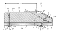
すなわち、アンテナ装置21において、ETC車載器のアンテナの一部として作用する放射素子2は、誘電体22の傾斜面22aに取付けられており、アンテナグランド4は、インサート成型されて誘電体22に内蔵されており、放射素子2と略平行に配置されている。このような構成により、この場合も、これら放射素子2およびアンテナグランド4は、回路基板23に対して傾斜角度θを有するように誘電体22で保持されている。
【0023】
GPS受信機のアンテナの一部として作用する放射素子24(本発明でいう他の放射素子)は、放射素子2と同様にして面状に形成されており、誘電体22の上面22bに取付けられている。放射素子2に電力を供給するための給電ピン8は、回路基板23に形成された貫通穴23cを貫通し、その端部8aが回路基板23の裏面23bではんだ9により導体パターン10にはんだ付けされて電気的に接続されている。また、放射素子24に電力を供給するための給電ピン25は、回路基板23に形成された貫通穴23dを貫通し、その端部25aが回路基板23の裏面23bではんだ26により導体パターン27にはんだ付けされて電気的に接続されている。
【0024】
ところで、以上は、GPS受信機のアンテナの一部として作用する放射素子24を備えた場合を説明したものであるが、この場合、GPS受信機のアンテナの一部として作用する放射素子24に代えて、例えばVICSのアンテナの一部として作用する放射素子や電話通信用のアンテナの一部として作用する放射素子を備える構成であっても良く、また、これら複数の放射素子を同時に備える構成であっても良い。
【0025】
以上に説明したように第3実施例によれば、アンテナ装置21において、放射素子2とアンテナグランド4とを回路基板23に対して傾斜角度θを有するように誘電体22で保持する構成としたので、上記した第1実施例に記載したものと同様にして、部品点数が増大することや取付作業が複雑になることを未然に回避することができ、しかも、このとき、傾斜角度θを任意に制御することにより、装置自体が大型化することなく、指向性パターンの最大利得角度を自在に制御することができる。また、この場合は、ETC車載器のアンテナの一部として作用する放射素子2に加えて、GPS受信機のアンテナの一部として作用する放射素子24をも一体に備える構成としたので、アンテナ装置21を多機能化することができる。
【0026】
(第4実施例)
次に、本発明の第4実施例について、図6および図7を参照して説明する。尚、上記した第3実施例と同一部分については説明を省略し、異なる部分について説明する。上記した第3実施例は、ETC車載器のアンテナの一部として作用する放射素子2とGPS受信機のアンテナの一部として作用する放射素子24とを隣接して配置するものであるが、これに対して、この第4実施例は、GPS受信機のアンテナの一部として作用する放射素子に中空部を形成し、ETC車載器のアンテナの一部として作用する放射素子をGPS受信機のアンテナの一部として作用する放射素子の中空部に配置するものである。
【0027】
すなわち、アンテナ装置31において、GPS受信機のアンテナの一部として作用する放射素子32(本発明でいう他の放射素子)は、中空部32aを有する形状となっており、誘電体33の上面33bに取付けられている。ETC車載器のアンテナの一部として作用する放射素子2は、放射素子32に形成された中空部32aに配置され、誘電体33の傾斜面33aに取付けられており、アンテナグランド4は、インサート成型されて誘電体33に内蔵されており、放射素子2と略平行に配置されている。このような構成により、この場合も、これら放射素子2およびアンテナグランド4は、回路基板34に対して傾斜角度θを有するように誘電体33で保持されている。
【0028】
放射素子2に電力を供給するための給電ピン8は、回路基板34に形成された貫通穴34cを貫通し、その端部8aが回路基板34の裏面34bではんだ9により導体パターン10にはんだ付けされて電気的に接続されている。また、放射素子32に電力を供給するための給電ピン35は、回路基板34に形成された貫通穴34dを貫通し、その端部35aが回路基板34の裏面34bではんだ36により導体パターン37にはんだ付けされて電気的に接続されている。
【0029】
尚、この場合、上記した第3実施例で説明したGPS受信機のアンテナの一部として作用する放射素子24の外形寸法(図4および図5中、L1にて示す)と、この第4実施例で説明したGPS受信機のアンテナの一部として作用する放射素子32の外形寸法(図6および図7中、L2にて示す)とは同一であり、つまり、この第4実施例では、ETC車載器のアンテナの一部として作用する放射素子2を放射素子32に形成された中空部32aに配置する分、上記した第3実施例に記載したものよりも、装置自体を小型化することができる。
【0030】
以上に説明したように第4実施例によれば、アンテナ装置31において、放射素子2とアンテナグランド4とを回路基板34に対して傾斜角度θを有するように誘電体33で保持する構成としたので、上記した第1実施例に記載したものと同様にして、部品点数が増大することや取付作業が複雑になることを未然に回避することができ、しかも、このとき、傾斜角度θを任意に制御することにより、装置自体が大型化することなく、指向性パターンの最大利得角度を自在に制御することができる。また、この場合は、ETC車載器のアンテナの一部として作用する放射素子2に加えて、GPS受信機のアンテナの一部として作用する放射素子32をも一体に備える構成としたので、上記した第3実施例に記載したものと同様にして、アンテナ装置31を多機能化することができ、さらに、GPS受信機のアンテナの一部として作用する放射素子32に中空部32aを形成し、ETC車載器のアンテナの一部として作用する放射素子2を中空部32aに配置する構成としたので、装置自体を小型化することをもできる。
【0031】
(その他の実施例)
本発明は、上記した実施例にのみ限定されるものではなく、以下のように変形または拡張することができる。
誘電体は、樹脂やセラミックからなるものに限らず、他の材質からなるものであっても良い。
第3実施例および第4実施例において、ETC車載器のアンテナの一部として作用する放射素子が取付けられる誘電体と、GPS受信機のアンテナの一部として作用する放射素子が取付けられる誘電体とが別体の構成であっても良い。
【図面の簡単な説明】
【図1】本発明の第1実施例を示す縦断側面図
【図2】放射素子およびアンテナグランドの回路基板に対する傾斜角度と、指向性パターンの最大利得角度との関係を示すグラフ
【図3】本発明の第2実施例を示す縦断側面図
【図4】本発明の第3実施例を示す縦断側面図
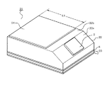
【図5】外観斜視図
【図6】本発明の第4実施例を示す縦断側面図
【図7】図5相当図
【符号の説明】
図面中、1はアンテナ装置、2は放射素子、3は誘電体、4はアンテナグランド、5は回路基板、11はアンテナ装置、12は誘電体、21はアンテナ装置、22は誘電体、23は回路基板、24は放射素子(他の放射素子)、31はアンテナ装置、32は放射素子(他の放射素子)、33は誘電体、34は回路基板である。[0001]
TECHNICAL FIELD OF THE INVENTION
The present invention relates to an antenna device having a dielectric between a radiating element and an antenna ground.
[0002]
[Prior art]
Conventionally, there is a configuration in which a radiating element is mounted so as to have a predetermined inclination angle with respect to a circuit board (for example, see Patent Documents 1 and 2).
[0003]
[Patent Document 1]
JP-A-2002-111377
[Patent Document 2]
JP 2001-159672 A
[Problems to be solved by the invention]
However, in the configurations described in
[0006]
The present invention has been made in view of the above circumstances, and an object of the present invention is to prevent an increase in the number of parts and a complicated mounting operation beforehand, and furthermore, an increase in the size of the device itself. An object of the present invention is to provide an antenna device that can freely control the maximum gain angle of the directivity pattern without performing the above operation.
[0007]
[Means for Solving the Problems]
According to the antenna device of the first aspect, the dielectric element is originally disposed for the purpose of facilitating the passage of the electric flux between the radiating element and the antenna ground and contributing to the miniaturization of the device itself. Since the radiating element and the antenna ground have a predetermined inclination angle with respect to the circuit board, the antenna pedestal and the bracket are different from the conventional one in which the radiating element is held by the antenna pedestal and the bracket. Since the number of parts can be eliminated, an increase in the number of parts and a complicated mounting operation can be avoided. Moreover, at this time, by arbitrarily controlling the predetermined inclination angle, the maximum gain angle of the directivity pattern can be freely controlled without increasing the size of the device itself.
[0008]
According to the antenna device of the second aspect, since the dielectric is made of resin and the antenna ground is insert-molded in the resin, the antenna ground can be appropriately fixed to the dielectric by insert molding.
[0009]
According to the antenna device of the third aspect, since the other radiating element is integrally provided, the antenna device can be multifunctional.
[0010]
BEST MODE FOR CARRYING OUT THE INVENTION
(First embodiment)
Hereinafter, a first embodiment of the present invention will be described with reference to FIGS.
FIG. 1 shows a longitudinal side view of the antenna device 1. In the antenna device 1, the
[0011]
The circuit board 5 has a circuit board ground 6 formed on its
[0012]
In this case, the antenna device 1 can be manufactured by the following procedure. That is, the
[0013]
Here, FIG. 2 is a graph showing the relationship between the inclination angle θ of the
[0014]
Thereby, the maximum gain angle of the directivity pattern can be freely controlled by arbitrarily setting the inclination angle θ of the
[0015]
As described above, according to the first embodiment, in the antenna device 1, the
[0016]
In this case, since the dielectric 3 is made of resin and the antenna ground 4 is insert-molded into resin, the antenna ground 4 can be appropriately fixed to the dielectric 3 by insert molding.
[0017]
(Second embodiment)
Next, a second embodiment of the present invention will be described with reference to FIG. The description of the same parts as in the first embodiment will be omitted, and different parts will be described.
[0018]
In the above-described first embodiment, the dielectric 3 is made of resin, and the antenna ground 4 is insert-molded and built in the dielectric 3. On the other hand, in the second embodiment, The dielectric is made of ceramic.
[0019]
That is, in the
[0020]
As described above, according to the second embodiment, only the material of the dielectric 12 is different from that described in the first embodiment, and the
[0021]
(Third embodiment)
Next, a third embodiment of the present invention will be described with reference to FIGS. Also in this case, the description of the same parts as those in the first embodiment will be omitted, and different parts will be described. The first embodiment has only the radiating
[0022]
That is, in the
[0023]
The radiating element 24 (other radiating element in the present invention) acting as a part of the antenna of the GPS receiver is formed in a planar shape in the same manner as the radiating
[0024]
By the way, the case where the radiating
[0025]
As described above, according to the third embodiment, in the
[0026]
(Fourth embodiment)
Next, a fourth embodiment of the present invention will be described with reference to FIGS. The description of the same parts as in the third embodiment is omitted, and different parts will be described. In the third embodiment described above, the radiating
[0027]
That is, in the
[0028]
The
[0029]
In this case, the outer dimensions (indicated by L1 in FIGS. 4 and 5) of the radiating
[0030]
As described above, according to the fourth embodiment, in the
[0031]
(Other Examples)
The present invention is not limited to the above-described embodiment, but can be modified or expanded as follows.
The dielectric is not limited to one made of resin or ceramic, and may be made of another material.
In the third and fourth embodiments, the dielectric to which the radiating element acting as a part of the antenna of the vehicle-mounted ETC is attached, and the dielectric to which the radiating element acting as part of the antenna of the GPS receiver is attached May be a separate structure.
[Brief description of the drawings]
FIG. 1 is a longitudinal sectional side view showing a first embodiment of the present invention. FIG. 2 is a graph showing a relationship between an inclination angle of a radiating element and an antenna ground with respect to a circuit board and a maximum gain angle of a directivity pattern. FIG. 4 is a vertical side view showing a second embodiment of the present invention. FIG. 4 is a vertical side view showing a third embodiment of the present invention. FIG. 5 is an external perspective view. FIG. 6 is a vertical side view showing a fourth embodiment of the present invention. FIG. 7 FIG. 5 equivalent diagram [Description of reference numerals]
In the drawing, 1 is an antenna device, 2 is a radiating element, 3 is a dielectric, 4 is an antenna ground, 5 is a circuit board, 11 is an antenna device, 12 is a dielectric, 21 is an antenna device, 22 is a dielectric, 23 is A circuit board, 24 is a radiating element (other radiating element), 31 is an antenna device, 32 is a radiating element (other radiating element), 33 is a dielectric, and 34 is a circuit board.
Claims (6)
前記放射素子と前記アンテナグランドとを回路基板に対して所定の傾斜角度を有するように前記誘電体で保持したことを特徴とするアンテナ装置。An antenna device in which a dielectric is interposed between a radiating element and an antenna ground,
An antenna device, wherein the radiating element and the antenna ground are held by the dielectric so as to have a predetermined inclination angle with respect to a circuit board.
前記誘電体を樹脂から構成し、前記アンテナグランドを前記樹脂にインサート成型したことを特徴とするアンテナ装置。The antenna device according to claim 1,
An antenna device, wherein the dielectric is made of resin, and the antenna ground is insert-molded in the resin.
他の放射素子を一体に備えたことを特徴とするアンテナ装置。The antenna device according to claim 1 or 2,
An antenna device comprising another radiating element integrally.
前記放射素子と前記他の放射素子とを隣接して配置したことを特徴とするアンテナ装置。The antenna device according to claim 3,
An antenna device, wherein the radiating element and the other radiating element are arranged adjacent to each other.
前記他の放射素子に中空部を形成し、前記放射素子を前記他の放射素子における前記中空部に配置したことを特徴とするアンテナ装置。The antenna device according to claim 3,
An antenna device, wherein a hollow portion is formed in the other radiating element, and the radiating element is arranged in the hollow portion of the other radiating element.
前記放射素子は、ETC車載器のアンテナの一部として作用するものであることを特徴とするアンテナ装置。The antenna device according to any one of claims 1 to 5,
The antenna device, wherein the radiating element functions as a part of an antenna of an on-board ETC device.
Priority Applications (2)
| Application Number | Priority Date | Filing Date | Title |
|---|---|---|---|
| JP2003018869A JP2004235729A (en) | 2003-01-28 | 2003-01-28 | Antenna device |
| US10/765,762 US6975270B2 (en) | 2003-01-28 | 2004-01-26 | Antenna unit |
Applications Claiming Priority (1)
| Application Number | Priority Date | Filing Date | Title |
|---|---|---|---|
| JP2003018869A JP2004235729A (en) | 2003-01-28 | 2003-01-28 | Antenna device |
Publications (1)
| Publication Number | Publication Date |
|---|---|
| JP2004235729A true JP2004235729A (en) | 2004-08-19 |
Family
ID=32820595
Family Applications (1)
| Application Number | Title | Priority Date | Filing Date |
|---|---|---|---|
| JP2003018869A Pending JP2004235729A (en) | 2003-01-28 | 2003-01-28 | Antenna device |
Country Status (2)
| Country | Link |
|---|---|
| US (1) | US6975270B2 (en) |
| JP (1) | JP2004235729A (en) |
Cited By (8)
| Publication number | Priority date | Publication date | Assignee | Title |
|---|---|---|---|---|
| JP2007067784A (en) * | 2005-08-31 | 2007-03-15 | Furukawa Electric Co Ltd:The | Multi-frequency integrated antenna |
| JP2007104257A (en) * | 2005-10-04 | 2007-04-19 | Yokowo Co Ltd | Dielectric antenna and element therefor |
| JP2010081500A (en) * | 2008-09-29 | 2010-04-08 | Nippon Antenna Co Ltd | Integrated antenna |
| WO2013094692A1 (en) * | 2011-12-20 | 2013-06-27 | 株式会社フジクラ | Antenna device |
| JP2014062845A (en) * | 2012-09-24 | 2014-04-10 | Seiko Epson Corp | Built-in antenna electronic clock |
| WO2015087486A1 (en) * | 2013-12-10 | 2015-06-18 | パナソニック株式会社 | Wireless module |
| KR101819173B1 (en) * | 2016-02-05 | 2018-01-17 | 한국전기연구원 | Cavity-backed coupler with enhanced coupling sensitivity |
| WO2023286610A1 (en) * | 2021-07-12 | 2023-01-19 | 株式会社村田製作所 | Antenna device and communication module |
Families Citing this family (5)
| Publication number | Priority date | Publication date | Assignee | Title |
|---|---|---|---|---|
| US7245261B2 (en) * | 2005-07-12 | 2007-07-17 | Delphi Technologies, Inc. | Satellite diversity antenna system |
| EP3285332B1 (en) * | 2016-08-19 | 2019-04-03 | Swisscom AG | Antenna system |
| KR102280051B1 (en) * | 2018-08-22 | 2021-07-21 | 삼성전자주식회사 | Antenna module, and electronic device with the same |
| KR102537495B1 (en) | 2018-10-02 | 2023-05-26 | 삼성전자주식회사 | An electronic device including an antenna module |
| KR102707114B1 (en) * | 2019-10-11 | 2024-09-20 | 삼성전자주식회사 | A structure for fixing an antenna module and including the same |
Family Cites Families (4)
| Publication number | Priority date | Publication date | Assignee | Title |
|---|---|---|---|---|
| CN1094663C (en) * | 1994-03-08 | 2002-11-20 | 泰利泰尔有限责任公司 | Hand-held transmitting and/or receiving apparatus |
| JP3644331B2 (en) | 1999-12-03 | 2005-04-27 | 株式会社デンソー | GPS antenna device for portable terminal |
| JP2002111377A (en) | 2000-09-29 | 2002-04-12 | Mitsumi Electric Co Ltd | Antenna device |
| EP1237225A1 (en) * | 2001-03-01 | 2002-09-04 | Red-M (Communications) Limited | An antenna array |
-
2003
- 2003-01-28 JP JP2003018869A patent/JP2004235729A/en active Pending
-
2004
- 2004-01-26 US US10/765,762 patent/US6975270B2/en not_active Expired - Fee Related
Cited By (9)
| Publication number | Priority date | Publication date | Assignee | Title |
|---|---|---|---|---|
| JP2007067784A (en) * | 2005-08-31 | 2007-03-15 | Furukawa Electric Co Ltd:The | Multi-frequency integrated antenna |
| JP2007104257A (en) * | 2005-10-04 | 2007-04-19 | Yokowo Co Ltd | Dielectric antenna and element therefor |
| JP2010081500A (en) * | 2008-09-29 | 2010-04-08 | Nippon Antenna Co Ltd | Integrated antenna |
| WO2013094692A1 (en) * | 2011-12-20 | 2013-06-27 | 株式会社フジクラ | Antenna device |
| JP2014062845A (en) * | 2012-09-24 | 2014-04-10 | Seiko Epson Corp | Built-in antenna electronic clock |
| WO2015087486A1 (en) * | 2013-12-10 | 2015-06-18 | パナソニック株式会社 | Wireless module |
| KR101819173B1 (en) * | 2016-02-05 | 2018-01-17 | 한국전기연구원 | Cavity-backed coupler with enhanced coupling sensitivity |
| WO2023286610A1 (en) * | 2021-07-12 | 2023-01-19 | 株式会社村田製作所 | Antenna device and communication module |
| US12609452B2 (en) | 2021-07-12 | 2026-04-21 | Murata Manufacturing Co., Ltd. | Antenna device and communication module |
Also Published As
| Publication number | Publication date |
|---|---|
| US20040155821A1 (en) | 2004-08-12 |
| US6975270B2 (en) | 2005-12-13 |
Similar Documents
| Publication | Publication Date | Title |
|---|---|---|
| US7746286B2 (en) | Antenna device having good symmetry of directional characteristics | |
| JP2004235729A (en) | Antenna device | |
| JP2001085929A (en) | Asymmetric dipole antenna assembly | |
| JP2005039754A (en) | Antenna system | |
| KR100420489B1 (en) | A Compact Folded Patch Antenna | |
| JP2002111344A (en) | Portable radio | |
| JP4383411B2 (en) | Patch antenna | |
| JP6658889B2 (en) | Antenna and wireless module | |
| JP2009055299A (en) | Antenna and radio equipment | |
| JP5418688B2 (en) | Antenna device, antenna module, and portable terminal | |
| US6618015B2 (en) | Antenna for use with radio device | |
| US20120026059A1 (en) | Antenna device | |
| JP2008160411A (en) | Antenna device and portable radio | |
| KR20020091789A (en) | Built-in Patch Antenna for Mobile Communication Terminal and Method for Manufacturing it | |
| JP3880295B2 (en) | Chip antenna | |
| US20090303151A1 (en) | Low profile gps antenna assembly | |
| JP2006197449A (en) | Antenna device | |
| JP3983224B2 (en) | Patch antenna | |
| JP6004173B2 (en) | Antenna device | |
| JP2004241803A (en) | Radio communication apparatus | |
| JP2006128898A (en) | Antenna device | |
| JP4160948B2 (en) | Antenna device | |
| CN100569059C (en) | electronic device with wireless communication function | |
| JP2008219661A (en) | Antenna device | |
| JPH10233613A (en) | Antenna device and its mounting structure |
Legal Events
| Date | Code | Title | Description |
|---|---|---|---|
| A621 | Written request for application examination |
Free format text: JAPANESE INTERMEDIATE CODE: A621 Effective date: 20050621 |
|
| A977 | Report on retrieval |
Free format text: JAPANESE INTERMEDIATE CODE: A971007 Effective date: 20061101 |
|
| A131 | Notification of reasons for refusal |
Free format text: JAPANESE INTERMEDIATE CODE: A131 Effective date: 20061114 |
|
| A521 | Written amendment |
Free format text: JAPANESE INTERMEDIATE CODE: A523 Effective date: 20070115 |
|
| A131 | Notification of reasons for refusal |
Free format text: JAPANESE INTERMEDIATE CODE: A131 Effective date: 20070306 |
|
| A02 | Decision of refusal |
Free format text: JAPANESE INTERMEDIATE CODE: A02 Effective date: 20070821 |