JP2004236059A - Noise filter circuit for switching power source - Google Patents
Noise filter circuit for switching power source Download PDFInfo
- Publication number
- JP2004236059A JP2004236059A JP2003023112A JP2003023112A JP2004236059A JP 2004236059 A JP2004236059 A JP 2004236059A JP 2003023112 A JP2003023112 A JP 2003023112A JP 2003023112 A JP2003023112 A JP 2003023112A JP 2004236059 A JP2004236059 A JP 2004236059A
- Authority
- JP
- Japan
- Prior art keywords
- line
- capacitor
- noise filter
- switching power
- short
- Prior art date
- Legal status (The legal status is an assumption and is not a legal conclusion. Google has not performed a legal analysis and makes no representation as to the accuracy of the status listed.)
- Pending
Links
- 239000003990 capacitor Substances 0.000 claims abstract description 60
- 239000004020 conductor Substances 0.000 abstract description 25
- 230000007935 neutral effect Effects 0.000 description 17
- 238000009499 grossing Methods 0.000 description 4
- 238000010586 diagram Methods 0.000 description 3
- 230000002159 abnormal effect Effects 0.000 description 1
- 230000005856 abnormality Effects 0.000 description 1
- 230000000694 effects Effects 0.000 description 1
- 238000012986 modification Methods 0.000 description 1
- 230000004048 modification Effects 0.000 description 1
- 230000003071 parasitic effect Effects 0.000 description 1
- 230000002250 progressing effect Effects 0.000 description 1
Images


Landscapes
- Filters And Equalizers (AREA)
- Dc-Dc Converters (AREA)
Abstract
Description
【0001】
【産業上の利用分野】
この発明は、スイッチング電源用のノイズフィルタ回路に関する。
【0002】
【従来の技術】
スイッチング電源回路には、入力側から侵入する外来ノイズからスイッチング電源回路を保護するため、あるいはAC入力端に現れるスイッチング電源回路からの伝導ノイズを抑制するためにノイズフィルタ回路が設けられている。
【0003】
図1は、スイッチング電源回路の構成を示している。
【0004】
スイッチング電源回路は、入力部1、ノイズフィルタ部(ノイズフィルタ回路)2、整流平滑部3およびコンバータ部4から構成されている。入力された交流電圧は、整流平滑部3によって整流および平滑化された後、コンバータ部4で変換されて所定の直流電圧を出力する。
【0005】
商用交流電源からの商用交流電力は、ライン(ライン線)Lとニュートラル(中性線)Nとからなる交流供給線によって送られる。入力部1では、ラインLに過電流保護用ヒューズF1が接続されている。
【0006】
ノイズフィルタ部2では、ヒューズF1の後のラインLとニュートラルNとの間に、LとNとの間の高周波ノイズを低減させるためのアクロスザラインコンデンサC1が接続されている。その後段には、ラインLとフレームグランド(グランド線)FGとの間に、LとFGとの間の高周波ノイズを低減させるためのラインバイパスコンデンサC3が接続されているとともにニュートラルNとフレームグランドFGとの間に、NとFGとの間の高周波ノイズを低減させるためのラインバイパスコンデンサC4が接続されている。
【0007】
その後段に、ラインLとニュートラルNとの間に、同相成分のノイズを除去するためのチョークコイルL1が接続されている。
【0008】
チョークコイルL1の後段においても、ヒューズF1の後のラインLとニュートラルNとの間に、アクロスザラインコンデンサC2が接続されている。そして、その後段に、ラインLとフレームグランドFGとの間に、ラインバイパスコンデンサC5が接続されているとともにニュートラルNとフレームグランドFGとの間にラインバイパスコンデンサC6が接続されている。
【0009】
ノイズフィルタ部2内のラインバイパスコンデンサC3、C4、C5、C6は、DC−DCコンバータ内のスイッチング素子(図示略)のコレクタあるいはソースとフレームグランドFG間の寄生キャパシタを通して流れる電流によって発生するコモンモードノイズを除去するものである。
【0010】
ノイズフィルタ部2を通過した交流入力は、整流平滑部3内のダイオードブリッジDによって整流された後、整流平滑部3内のダイオードC7によって平滑化されて、非安定直流電圧となる。この非安定直流電圧は、コンバータ部内のDC−DCコンバータによって安定化されて所定の直流電圧なって出力される。
【0011】
【特許文献1】特開平8−191570号公報
【特許文献2】特開平7−39136号公報
【特許文献3】特開1994−153382号公報
【特許文献4】特開2000−98797号公報
【0012】
【発明が解決しようとする課題】
安全規格上、上記ノイズフィルタ部2内の各コンデンサの異常時を考慮して、素子の短絡試験を実施することにより、回路基板上の導体パターン焼損等によって危険な状態にならないようにしている。
【0013】
ラインバイパスコンデンサC3、C4、C5、C6に対しても異常試験が実施され、これらの素子が短絡した場合にも、ラインLまたはニュートラルNからコンデンサまでの導体パターンおよび各コンデンサからフレームグランドFGまでの導体パターンが焼損しないように、これらの導体パターンの幅を大きくしている。
【0014】
つまり、ラインバイパスコンデンサが短絡した場合において、過電流保護用ヒューズF1が溶断するまでに、上記導体パターンが焼損してしまわないように、上記導体パターンの幅を大きくしている。例えば、交流電源電圧が100Vの国内向けの仕様には、過電流保護用ヒューズF1として15Aのヒューズがよく用いられるため、上記導体パターンの幅としては、20mm以上が必要とされていることが多い。
【0015】
しかしながら、機器の小型化が進んでいるため、スイッチング電源回路にも小型化が要求されるが、従来回路では上述したように導体パターンの幅を大きくとる必要があるため、機器を小型化することが困難となっている。
【0016】
この発明は、導体パターンの幅を小さくでき、しかもラインバイパスコンデンサが短絡した場合において、導体パターンが焼損しないようにできるスイッチング電源用のノイズフィルタ回路を提供することを目的とする。
【0017】
【課題を解決するための手段】
請求項1に記載の発明は、交流供給線とグランド線との間に接続されたラインバイパスコンデンサを備えているスイッチング電源用のノイズフィルタ回路において、ラインバイパスコンデンサが接続されている交流供給線とグランド線との間において、ラインバイパスコンデンサと直列にコンデンサ短絡時用ヒューズが接続されていることを特徴とする。交流供給線には、図1〜図3のライン(ライン線)Lおよびニュートラル(中性線)Nが含まれる。
【0018】
【発明の実施の形態】
以下、図2および図3を参照して、この発明の実施の形態について説明する。
【0019】
図2は、スイッチング電源回路の構成を示している。図2において、図1と同じものには、同じ符号を付してその説明を省略する。
【0020】
このスイッチング電源回路では、ノイズフィルタ部2Aの構成が図1のノイズフィルタ部2の構成と異なっている。このノイズフィルタ部2Aでは、ラインバイパスコンデンサC3、C4とフレームグランドFGとの間に、コンデンサ短絡時用ヒューズF2が接続されているとともに、ラインバイパスコンデンサC5、C6とフレームグランドFGとの間に、コンデンサ短絡時用ヒューズF3が接続されている。
【0021】
この例では、交流電源電圧が100Vであり、過電流保護用ヒューズF1として15Aのヒューズが用いられているとすると、コンデンサ短絡時用ヒューズF2、F3としては、例えば、1Aのヒューズが用いられる。
【0022】
図2のノイズフィルタ部2Aにおいては、ラインバイパスコンデンサC3が短絡した場合には、直ちに、コンデンサ短絡時用ヒューズF2が溶断する。このため、ラインLからコンデンサC3までの導体パターンおよびコンデンサC3からフレームグランドFGまでの導体パターンに大きな電流が流れるのが回避される。ラインバイパスコンデンサC4が短絡した場合には、直ちに、コンデンサ短絡時用ヒューズF2が溶断する。このため、ニュートラルNからコンデンサC4までの導体パターンおよびコンデンサC4からフレームグランドFGまでの導体パターンに大きな電流が流れるのが回避される。
【0023】
ラインバイパスコンデンサC5が短絡した場合には、直ちに、コンデンサ短絡時用ヒューズF3が溶断する。このため、ラインLからコンデンサC5までの導体パターンおよびコンデンサC5からフレームグランドFGまでの導体パターンに大きな電流が流れるのが回避される。ラインバイパスコンデンサC6が短絡した場合には、直ちに、コンデンサ短絡時用ヒューズF3が溶断する。このため、ニュートラルNからコンデンサC6までの導体パターンおよびコンデンサC6からフレームグランドFGまでの導体パターンに大きな電流が流れるのが回避される。
【0024】
つまり、ラインバイパスコンデンサC3、C4、C5、C6が短絡した場合にも、ラインLまたはニュートラルNからコンデンサまでの導体パターンおよび各コンデンサからフレームグランドFGまでの導体パターンに大電流が流れないため、これらの導体パターンの幅を図1のノイズフィルタ部2に比べて小さくすることが可能となる。この結果、スイッチング電源回路の小型化を図ることができる。
【0025】
なお、図2に示すようなコンデンサ短絡時用ヒューズF2、F3を設ける代わりに、図3に示すノイズフィルタ部2Bのように、コンデンサC3とラインLとの間にコンデンサ短絡時用ヒューズF4を、コンデンサC4とニュートラルNとの間にコンデンサ短絡時用ヒューズF5を、コンデンサC5とラインLとの間にコンデンサ短絡時用ヒューズF6を、コンデンサC6とニュートラルNとの間にコンデンサ短絡時用ヒューズF6を、設けてもよい。
【0026】
【発明の効果】
この発明によれば、導体パターンの幅を小さくでき、しかもラインバイパスコンデンサが短絡した場合において、導体パターンが焼損しないようにできる。
【図面の簡単な説明】
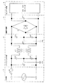
【図1】従来のスイッチング電源回路の構成を示す電気回路図である。
【図2】実施の形態であるスイッチング電源回路の構成を示す電気回路図である。
【図3】変形例を示す電気回路図である。
【符号の説明】
2A、2B ノイズフィルタ部
L ライン(ライン線)
N ニュートラル(中性線)
FG フレームグランド(グランド線)
C3、C4、C5、C6 ラインバイパスコンデンサ
F2、F3、F4、F5、F6、F7 コンデンサ短絡時用ヒューズ[0001]
[Industrial applications]
The present invention relates to a noise filter circuit for a switching power supply.
[0002]
[Prior art]
The switching power supply circuit is provided with a noise filter circuit for protecting the switching power supply circuit from external noise invading from the input side or for suppressing conduction noise from the switching power supply circuit appearing at the AC input terminal.
[0003]
FIG. 1 shows the configuration of the switching power supply circuit.
[0004]
The switching power supply circuit includes an
[0005]
Commercial AC power from a commercial AC power supply is sent by an AC supply line composed of a line (line line) L and a neutral (neutral line) N. In the
[0006]
In the
[0007]
In the subsequent stage, a choke coil L1 for removing in-phase component noise is connected between the line L and the neutral N.
[0008]
In the subsequent stage of the choke coil L1, an across-the-line capacitor C2 is connected between the line L after the fuse F1 and the neutral N. In the subsequent stage, a line bypass capacitor C5 is connected between the line L and the frame ground FG, and a line bypass capacitor C6 is connected between the neutral N and the frame ground FG.
[0009]
The line bypass capacitors C3, C4, C5, and C6 in the
[0010]
The AC input that has passed through the
[0011]
[Patent Document 1] JP-A-8-191570 [Patent Document 2] JP-A-7-39136 [Patent Document 3] JP-A-1994-153382 [Patent Document 4] JP-A-2000-98797 ]
[Problems to be solved by the invention]
According to safety standards, a short circuit test of the elements is performed in consideration of abnormal times of each capacitor in the
[0013]
Abnormality tests are also performed on the line bypass capacitors C3, C4, C5, and C6. Even when these elements are short-circuited, the conductor pattern from the line L or the neutral N to the capacitor and the conductor pattern from each capacitor to the frame ground FG can be obtained. The width of these conductor patterns is increased so that the conductor patterns do not burn out.
[0014]
That is, when the line bypass capacitor is short-circuited, the width of the conductor pattern is increased so that the conductor pattern does not burn out before the overcurrent protection fuse F1 is blown. For example, in a domestic specification having an AC power supply voltage of 100 V, a fuse of 15 A is often used as the overcurrent protection fuse F1, and therefore, the width of the conductor pattern is often required to be 20 mm or more. .
[0015]
However, as the miniaturization of equipment is progressing, the switching power supply circuit is also required to be miniaturized.However, in the conventional circuit, it is necessary to increase the width of the conductor pattern as described above. Has become difficult.
[0016]
SUMMARY OF THE INVENTION It is an object of the present invention to provide a noise filter circuit for a switching power supply that can reduce the width of a conductor pattern and can prevent the conductor pattern from being burned out when a line bypass capacitor is short-circuited.
[0017]
[Means for Solving the Problems]
According to a first aspect of the present invention, there is provided a noise filter circuit for a switching power supply including a line bypass capacitor connected between an AC supply line and a ground line, wherein the AC supply line to which the line bypass capacitor is connected is provided. A fuse for short-circuiting the capacitor is connected in series with the line bypass capacitor between the ground line and the ground line. The AC supply line includes the line (line line) L and the neutral (neutral line) N in FIGS.
[0018]
BEST MODE FOR CARRYING OUT THE INVENTION
An embodiment of the present invention will be described below with reference to FIGS.
[0019]
FIG. 2 shows the configuration of the switching power supply circuit. 2, the same components as those in FIG. 1 are denoted by the same reference numerals, and description thereof will be omitted.
[0020]
In this switching power supply circuit, the configuration of the noise filter unit 2A is different from the configuration of the
[0021]
In this example, assuming that the AC power supply voltage is 100 V and a 15-A fuse is used as the overcurrent protection fuse F1, for example, a 1-A fuse is used as the capacitor short-circuit fuses F2 and F3.
[0022]
In the noise filter section 2A of FIG. 2, when the line bypass capacitor C3 is short-circuited, the capacitor short-circuit fuse F2 is blown immediately. Therefore, it is possible to prevent a large current from flowing through the conductor pattern from the line L to the capacitor C3 and the conductor pattern from the capacitor C3 to the frame ground FG. When the line bypass capacitor C4 is short-circuited, the capacitor short-circuit fuse F2 is blown immediately. Therefore, a large current is prevented from flowing through the conductor pattern from the neutral N to the capacitor C4 and the conductor pattern from the capacitor C4 to the frame ground FG.
[0023]
When the line bypass capacitor C5 is short-circuited, the capacitor short-circuit fuse F3 is blown immediately. Therefore, it is possible to prevent a large current from flowing through the conductor pattern from the line L to the capacitor C5 and the conductor pattern from the capacitor C5 to the frame ground FG. When the line bypass capacitor C6 is short-circuited, the capacitor short-circuit fuse F3 is blown immediately. For this reason, a large current is prevented from flowing through the conductor pattern from the neutral N to the capacitor C6 and the conductor pattern from the capacitor C6 to the frame ground FG.
[0024]
That is, even when the line bypass capacitors C3, C4, C5, and C6 are short-circuited, a large current does not flow through the conductor pattern from the line L or the neutral N to the capacitor and the conductor pattern from each capacitor to the frame ground FG. Can be made smaller than the width of the
[0025]
Note that instead of providing the capacitor short-circuit fuses F2 and F3 as shown in FIG. 2, a capacitor short-circuit fuse F4 is provided between the capacitor C3 and the line L as in a noise filter unit 2B shown in FIG. A fuse F5 for short-circuiting between the capacitor C4 and the neutral N, a fuse F6 for short-circuiting between the capacitor C5 and the line L, and a fuse F6 for short-circuiting between the capacitor C6 and the neutral N. , May be provided.
[0026]
【The invention's effect】
According to the present invention, the width of the conductor pattern can be reduced, and furthermore, the conductor pattern can be prevented from burning when the line bypass capacitor is short-circuited.
[Brief description of the drawings]
FIG. 1 is an electric circuit diagram showing a configuration of a conventional switching power supply circuit.
FIG. 2 is an electric circuit diagram showing a configuration of a switching power supply circuit according to the embodiment.
FIG. 3 is an electric circuit diagram showing a modification.
[Explanation of symbols]
2A, 2B Noise filter section L line (line line)
N neutral (neutral wire)
FG frame ground (ground line)
C3, C4, C5, C6 Line bypass capacitors F2, F3, F4, F5, F6, F7 Fuse for capacitor short circuit
Claims (1)
ラインバイパスコンデンサが接続されている交流供給線とグランド線との間において、ラインバイパスコンデンサと直列にコンデンサ短絡時用ヒューズが接続されていることを特徴とするスイッチング電源用のノイズフィルタ回路。In a noise filter circuit for a switching power supply having a line bypass capacitor connected between an AC supply line and a ground line,
A noise filter circuit for a switching power supply, wherein a capacitor short-circuit fuse is connected in series with a line bypass capacitor between an AC supply line to which a line bypass capacitor is connected and a ground line.
Priority Applications (1)
| Application Number | Priority Date | Filing Date | Title |
|---|---|---|---|
| JP2003023112A JP2004236059A (en) | 2003-01-31 | 2003-01-31 | Noise filter circuit for switching power source |
Applications Claiming Priority (1)
| Application Number | Priority Date | Filing Date | Title |
|---|---|---|---|
| JP2003023112A JP2004236059A (en) | 2003-01-31 | 2003-01-31 | Noise filter circuit for switching power source |
Publications (1)
| Publication Number | Publication Date |
|---|---|
| JP2004236059A true JP2004236059A (en) | 2004-08-19 |
Family
ID=32952014
Family Applications (1)
| Application Number | Title | Priority Date | Filing Date |
|---|---|---|---|
| JP2003023112A Pending JP2004236059A (en) | 2003-01-31 | 2003-01-31 | Noise filter circuit for switching power source |
Country Status (1)
| Country | Link |
|---|---|
| JP (1) | JP2004236059A (en) |
Cited By (6)
| Publication number | Priority date | Publication date | Assignee | Title |
|---|---|---|---|---|
| JP2008193788A (en) * | 2007-02-02 | 2008-08-21 | Tokyo Institute Of Technology | Power control device and vehicle equipped with the same |
| US7525826B2 (en) | 2006-04-21 | 2009-04-28 | Roland Corporation | Switching power supply apparatus and method |
| WO2014122736A1 (en) * | 2013-02-06 | 2014-08-14 | 三菱電機株式会社 | Filter device and electric rolling stock drive controller |
| JP2014217244A (en) * | 2013-04-30 | 2014-11-17 | 三菱電機株式会社 | Isolated switching power supply device and method of manufacturing isolated switching power supply device |
| JP2017212496A (en) * | 2016-05-23 | 2017-11-30 | 三菱電機エンジニアリング株式会社 | Filter circuit |
| JP6602518B1 (en) * | 2019-03-07 | 2019-11-06 | 三菱電機株式会社 | Noise filter circuit |
-
2003
- 2003-01-31 JP JP2003023112A patent/JP2004236059A/en active Pending
Cited By (9)
| Publication number | Priority date | Publication date | Assignee | Title |
|---|---|---|---|---|
| US7525826B2 (en) | 2006-04-21 | 2009-04-28 | Roland Corporation | Switching power supply apparatus and method |
| JP2008193788A (en) * | 2007-02-02 | 2008-08-21 | Tokyo Institute Of Technology | Power control device and vehicle equipped with the same |
| WO2014122736A1 (en) * | 2013-02-06 | 2014-08-14 | 三菱電機株式会社 | Filter device and electric rolling stock drive controller |
| CN104969466A (en) * | 2013-02-06 | 2015-10-07 | 三菱电机株式会社 | Filter device and electric vehicle drive control device |
| US9806691B2 (en) | 2013-02-06 | 2017-10-31 | Mitsubishi Electric Corporation | Filter device and electric-vehicle drive controller |
| JP2014217244A (en) * | 2013-04-30 | 2014-11-17 | 三菱電機株式会社 | Isolated switching power supply device and method of manufacturing isolated switching power supply device |
| JP2017212496A (en) * | 2016-05-23 | 2017-11-30 | 三菱電機エンジニアリング株式会社 | Filter circuit |
| JP6602518B1 (en) * | 2019-03-07 | 2019-11-06 | 三菱電機株式会社 | Noise filter circuit |
| WO2020179047A1 (en) * | 2019-03-07 | 2020-09-10 | 三菱電機株式会社 | Noise filter circuit |
Similar Documents
| Publication | Publication Date | Title |
|---|---|---|
| JP5170248B2 (en) | Power supply control circuit, power supply apparatus, power supply system, and control method for power supply control apparatus | |
| JP2004236059A (en) | Noise filter circuit for switching power source | |
| JP4662022B2 (en) | Matrix converter | |
| US20030173909A1 (en) | Power supply apparatus for light source | |
| JP2006060917A (en) | Noise filter circuit for switching power supply | |
| KR102260289B1 (en) | LED module power supply converter with surge voltage protection circuit | |
| JP2002198189A (en) | Electric discharge lamp lighting circuit | |
| JP2007295645A (en) | Switching power supply | |
| JP5233375B2 (en) | Rectified power supply circuit | |
| JP6466133B2 (en) | Electric circuit, electric compressor and electric circuit control method | |
| JP2004236413A (en) | Noise filter circuit for switching power supply | |
| JPH0422086A (en) | Protection circuit against surge voltage | |
| KR102260295B1 (en) | LED module power supply converter with PCB pattern-connected surge voltage protection circuit | |
| CN108667312B (en) | Electronic device | |
| JP3240031B2 (en) | DC high voltage power supply | |
| JP5583616B2 (en) | Switching power supply | |
| JP3806913B2 (en) | Power supply | |
| JP3931319B2 (en) | Power supply | |
| KR100948762B1 (en) | SMPS module with incorrect wiring protection | |
| CN210225276U (en) | a power supply device | |
| JP2909391B2 (en) | Inrush current suppression circuit | |
| JP4313963B2 (en) | Switching power supply | |
| JP2012005305A (en) | Protection circuit | |
| CN210380686U (en) | Flyback power supply circuit | |
| KR200421608Y1 (en) | Socket ballast for discharge lamp |
Legal Events
| Date | Code | Title | Description |
|---|---|---|---|
| A621 | Written request for application examination |
Effective date: 20050225 Free format text: JAPANESE INTERMEDIATE CODE: A621 |
|
| A131 | Notification of reasons for refusal |
Free format text: JAPANESE INTERMEDIATE CODE: A131 Effective date: 20080617 |
|
| A02 | Decision of refusal |
Free format text: JAPANESE INTERMEDIATE CODE: A02 Effective date: 20081106 |