JP2004240102A - Liquid crystal display substrate having phase difference control function and liquid crystal display using the same - Google Patents
Liquid crystal display substrate having phase difference control function and liquid crystal display using the same Download PDFInfo
- Publication number
- JP2004240102A JP2004240102A JP2003028176A JP2003028176A JP2004240102A JP 2004240102 A JP2004240102 A JP 2004240102A JP 2003028176 A JP2003028176 A JP 2003028176A JP 2003028176 A JP2003028176 A JP 2003028176A JP 2004240102 A JP2004240102 A JP 2004240102A
- Authority
- JP
- Japan
- Prior art keywords
- liquid crystal
- layer
- crystal display
- phase
- optical axis
- Prior art date
- Legal status (The legal status is an assumption and is not a legal conclusion. Google has not performed a legal analysis and makes no representation as to the accuracy of the status listed.)
- Granted
Links
Images



Classifications
-
- G—PHYSICS
- G02—OPTICS
- G02F—OPTICAL DEVICES OR ARRANGEMENTS FOR THE CONTROL OF LIGHT BY MODIFICATION OF THE OPTICAL PROPERTIES OF THE MEDIA OF THE ELEMENTS INVOLVED THEREIN; NON-LINEAR OPTICS; FREQUENCY-CHANGING OF LIGHT; OPTICAL LOGIC ELEMENTS; OPTICAL ANALOGUE/DIGITAL CONVERTERS
- G02F1/00—Devices or arrangements for the control of the intensity, colour, phase, polarisation or direction of light arriving from an independent light source, e.g. switching, gating or modulating; Non-linear optics
- G02F1/01—Devices or arrangements for the control of the intensity, colour, phase, polarisation or direction of light arriving from an independent light source, e.g. switching, gating or modulating; Non-linear optics for the control of the intensity, phase, polarisation or colour
- G02F1/13—Devices or arrangements for the control of the intensity, colour, phase, polarisation or direction of light arriving from an independent light source, e.g. switching, gating or modulating; Non-linear optics for the control of the intensity, phase, polarisation or colour based on liquid crystals, e.g. single liquid crystal display cells
- G02F1/133—Constructional arrangements; Operation of liquid crystal cells; Circuit arrangements
- G02F1/1333—Constructional arrangements; Manufacturing methods
- G02F1/1335—Structural association of cells with optical devices, e.g. polarisers or reflectors
- G02F1/13363—Birefringent elements, e.g. for optical compensation
-
- G—PHYSICS
- G02—OPTICS
- G02F—OPTICAL DEVICES OR ARRANGEMENTS FOR THE CONTROL OF LIGHT BY MODIFICATION OF THE OPTICAL PROPERTIES OF THE MEDIA OF THE ELEMENTS INVOLVED THEREIN; NON-LINEAR OPTICS; FREQUENCY-CHANGING OF LIGHT; OPTICAL LOGIC ELEMENTS; OPTICAL ANALOGUE/DIGITAL CONVERTERS
- G02F1/00—Devices or arrangements for the control of the intensity, colour, phase, polarisation or direction of light arriving from an independent light source, e.g. switching, gating or modulating; Non-linear optics
- G02F1/01—Devices or arrangements for the control of the intensity, colour, phase, polarisation or direction of light arriving from an independent light source, e.g. switching, gating or modulating; Non-linear optics for the control of the intensity, phase, polarisation or colour
- G02F1/13—Devices or arrangements for the control of the intensity, colour, phase, polarisation or direction of light arriving from an independent light source, e.g. switching, gating or modulating; Non-linear optics for the control of the intensity, phase, polarisation or colour based on liquid crystals, e.g. single liquid crystal display cells
- G02F1/133—Constructional arrangements; Operation of liquid crystal cells; Circuit arrangements
- G02F1/1333—Constructional arrangements; Manufacturing methods
- G02F1/1335—Structural association of cells with optical devices, e.g. polarisers or reflectors
- G02F1/13356—Structural association of cells with optical devices, e.g. polarisers or reflectors characterised by the placement of the optical elements
- G02F1/133565—Structural association of cells with optical devices, e.g. polarisers or reflectors characterised by the placement of the optical elements inside the LC elements, i.e. between the cell substrates
-
- G—PHYSICS
- G02—OPTICS
- G02F—OPTICAL DEVICES OR ARRANGEMENTS FOR THE CONTROL OF LIGHT BY MODIFICATION OF THE OPTICAL PROPERTIES OF THE MEDIA OF THE ELEMENTS INVOLVED THEREIN; NON-LINEAR OPTICS; FREQUENCY-CHANGING OF LIGHT; OPTICAL LOGIC ELEMENTS; OPTICAL ANALOGUE/DIGITAL CONVERTERS
- G02F1/00—Devices or arrangements for the control of the intensity, colour, phase, polarisation or direction of light arriving from an independent light source, e.g. switching, gating or modulating; Non-linear optics
- G02F1/01—Devices or arrangements for the control of the intensity, colour, phase, polarisation or direction of light arriving from an independent light source, e.g. switching, gating or modulating; Non-linear optics for the control of the intensity, phase, polarisation or colour
- G02F1/13—Devices or arrangements for the control of the intensity, colour, phase, polarisation or direction of light arriving from an independent light source, e.g. switching, gating or modulating; Non-linear optics for the control of the intensity, phase, polarisation or colour based on liquid crystals, e.g. single liquid crystal display cells
- G02F1/137—Devices or arrangements for the control of the intensity, colour, phase, polarisation or direction of light arriving from an independent light source, e.g. switching, gating or modulating; Non-linear optics for the control of the intensity, phase, polarisation or colour based on liquid crystals, e.g. single liquid crystal display cells characterised by the electro-optical or magneto-optical effect, e.g. field-induced phase transition, orientation effect, guest-host interaction or dynamic scattering
- G02F1/139—Devices or arrangements for the control of the intensity, colour, phase, polarisation or direction of light arriving from an independent light source, e.g. switching, gating or modulating; Non-linear optics for the control of the intensity, phase, polarisation or colour based on liquid crystals, e.g. single liquid crystal display cells characterised by the electro-optical or magneto-optical effect, e.g. field-induced phase transition, orientation effect, guest-host interaction or dynamic scattering based on orientation effects in which the liquid crystal remains transparent
- G02F1/1393—Devices or arrangements for the control of the intensity, colour, phase, polarisation or direction of light arriving from an independent light source, e.g. switching, gating or modulating; Non-linear optics for the control of the intensity, phase, polarisation or colour based on liquid crystals, e.g. single liquid crystal display cells characterised by the electro-optical or magneto-optical effect, e.g. field-induced phase transition, orientation effect, guest-host interaction or dynamic scattering based on orientation effects in which the liquid crystal remains transparent the birefringence of the liquid crystal being electrically controlled, e.g. ECB-, DAP-, HAN-, PI-LC cells
-
- G—PHYSICS
- G02—OPTICS
- G02F—OPTICAL DEVICES OR ARRANGEMENTS FOR THE CONTROL OF LIGHT BY MODIFICATION OF THE OPTICAL PROPERTIES OF THE MEDIA OF THE ELEMENTS INVOLVED THEREIN; NON-LINEAR OPTICS; FREQUENCY-CHANGING OF LIGHT; OPTICAL LOGIC ELEMENTS; OPTICAL ANALOGUE/DIGITAL CONVERTERS
- G02F2413/00—Indexing scheme related to G02F1/13363, i.e. to birefringent elements, e.g. for optical compensation, characterised by the number, position, orientation or value of the compensation plates
- G02F2413/02—Number of plates being 2
Landscapes
- Physics & Mathematics (AREA)
- Nonlinear Science (AREA)
- Mathematical Physics (AREA)
- Chemical & Material Sciences (AREA)
- Crystallography & Structural Chemistry (AREA)
- General Physics & Mathematics (AREA)
- Optics & Photonics (AREA)
- Liquid Crystal (AREA)
- Polarising Elements (AREA)
Abstract
【課題】位相差制御層をLCDを構成する基板の液晶層側に直接配置することにより、粘着材による界面反射をキャンセルさせて高コントラストな表示を可能にする。
【解決手段】液晶層を挟む透明基板1、1’の少なくとも何れか一方の内面に、重合性液晶分子からなる層面内に光軸を有する正の一軸性位相層a、若しくは、重合性液晶分子からなる層面の法線方向に光軸を有する負の一軸性位相層cの中、少なくとも一方がパターニングされて設けられている液晶ディスプレイ。
【選択図】 図1An object of the present invention is to arrange a phase difference control layer directly on a liquid crystal layer side of a substrate constituting an LCD, thereby canceling interfacial reflection by an adhesive and enabling a high-contrast display.
Kind Code: A1 A positive uniaxial phase layer a having an optical axis in a layer plane composed of polymerizable liquid crystal molecules on at least one of inner surfaces of transparent substrates 1 and 1 ′ sandwiching a liquid crystal layer, or polymerizable liquid crystal molecules. A liquid crystal display, wherein at least one of a negative uniaxial phase layer c having an optical axis in a direction normal to a layer surface is formed by patterning.
[Selection diagram] Fig. 1
Description
【0001】
【発明の属する技術分野】
本発明は、位相差制御機能を有する液晶ディスプレイ用基板及びそれを用いた液晶ディスプレイに関し、特に、液晶セル内部にパターニングされた位相差制御層を有する液晶ディスプレイ用基板とそれを用いた液晶ディスプレイに関するものである。
【0002】
【従来の技術】
カラー液晶ディスプレイ(以下、液晶ディスプレイをLCDと称す。)はその薄型、軽量、小消費電力、フリッカーレスといった特徴から、ノートパソコンを中心にその市場が急速に拡大してきた。最近になって、こうしたPC用途ディスプレイの一環として、ノートパソコンに比べてより大型のデスクトップ用モニターの需要が発生している。また、PC用のみならず、従来であればCRTが主流であったTV向けにも、LCDが利用されるようになってきた。
【0003】
ここで、LCDの問題点として、その狭い視野角度の問題がある。これは、斜め方向からLCDを観察した場合、元来黒を表示すべき画素からの光漏れが生じるためであり、それが原因でコントラストの反転が生じ、正しい表示ができなくなるためである。このような問題点に鑑み、特許文献1、特許文献2のように、位相差フィルムを用いて、黒表示画素において視野角度が増大した場合でも、光漏れが生じない、広視野角度な垂直配向モードLCDが考案されている。
【0004】
【特許文献1】
特開平10−153802号公報
【0005】
【特許文献2】
特開平11−258605号公報
【0006】
【特許文献3】
特開平7−258638号公報
【0007】
【特許文献4】
特表平10−508882号公報
【0008】
【発明が解決しようとする課題】
これらの位相差フィルムは、通常、偏光板と互いの光軸(偏光板の場合は吸収軸、位相差フィルムの場合は光学軸)をある特定の角度をなすように貼り合わせて用いられる。しかしながら、その際に使用される粘着剤はその屈折率が偏光板、位相差板(位相差フィルム)に比較して小さいため、界面で光の反射が生じ、表示のコントラストが低下するといった問題点があった。
【0009】
また、一般に、位相差補償には波長分散が伴うため、ある特定波長を中心に補償を行っている。多くの場合では、視感度の最も高い緑を中心に位相差補償の設計がなされる。そのため、黒表示画素を完全な黒状態として表示できず、赤色と青色の光成分が漏れるため、紫がかった黒表示になってしまう。
【0010】
その他にも、位相差フィルムは吸湿することにより体積変化を生じるので、位相差に変化が生じ、LCDに適用した場合は画面が歪むといった欠点がある。この傾向は、位相差フィルムの面積が大きくなる程顕著になり、近年応用が進んでいる液晶TVにおいて特に問題となる。
【0011】
本発明は従来技術のこのような問題点に鑑みてなされたものであり、その目的は、通常フィルム状態として用いられる位相差制御層をLCDを構成する基板の液晶層側に直接配置することにより、粘着材による界面反射をキャンセルさせて高コントラストな表示を可能にすることである。
【0012】
また、インセル構造でかつ直接透明基板、カラーフィルター等の基材に積層可能にして、従来の位相差フィルムに見られるような吸湿による体積変化を生じさせなるようにすることである。
【0013】
また、さらに、本発明においては、位相差制御層をR(赤色)、G(緑色)、B(青色)に対応する各領域にパターニングすることにより、それぞれの色の画素領域で位相差を別々に制御し、波長分散のない位相差補償を可能にすることである。
【0014】
【課題を解決するための手段】
上記目的を達成する本発明の位相差制御機能を有する液晶ディスプレイ用基板は、液晶ディスプレイの液晶層を挟む透明基板において、その液晶層側に、重合性液晶分子からなる層面内に光軸を有する正の一軸性位相層、若しくは、重合性液晶分子からなる層面の法線方向に光軸を有する負の一軸性位相層の中、少なくとも一方がパターニングされて設けられていることを特徴とするものである。
【0015】
この場合、重合性液晶分子からなる層面の法線方向に光軸を有する負の一軸性位相層は、重合性液晶分子とカイラル剤の混合物からなることが望ましい。
【0016】
本発明のもう1つの位相差制御機能を有する液晶ディスプレイ用基板は、液晶ディスプレイの液晶層を挟む透明基板において、その液晶層側に、配向膜、重合性液晶分子からなる層面内に光軸を有する正の一軸性位相層、重合性液晶分子からなる層面の法線方向に光軸を有する負の一軸性位相層の順に積層されていることを特徴とするものである。
【0017】
この場合に、重合性液晶分子からなる層面内に光軸を有する正の一軸性位相層と、重合性液晶分子からなる層面の法線方向に光軸を有する負の一軸性位相層の間に配向膜を有することが望ましい。
【0018】
また、第1の位相差制御機能を有する液晶ディスプレイ用基板において、層面内に光軸を有する正の一軸性位相層、若しくは、層面の法線方向に光軸を有する負の一軸性位相層の一方がフィルム状態で液晶ディスプレイの液晶層を挟む透明基板の液晶層とは反対側に貼り付けられているものとすることも可能である。
【0019】
以上において、重合性液晶分子からなる層面内に光学的に正の一軸性を有する位相層、若しくは、重合性液晶分子からなる層面の法線方向に光学的に負の一軸性を有する位相層の中、少なくとも一方がパターニングされてなる位相差制御機能を有する液晶ディスプレイ用基板が、R、G、B3色の領域を有し、かつ、その位相差層の中、少なくとも一方がそのR、G、B3色の領域に合わせてパターニングされて形成されていることが望ましい。
【0020】
以上において、液晶層の配向モードが垂直配向モードであるものを対象とすることが望ましい。
【0021】
その場合に、垂直配向モードである液晶層に用いる液晶分子の屈折率異方性が0.05から0.30であり、かつ、位相層として用いる重合性液晶分子の屈折率異方性が0.05から0.30であるのが一般的てあり、また、垂直配向モードである液晶層の厚さが1.0μmから6.0μmであり、かつ、重合性液晶分子からなる位相層の膜厚は0.1μmから10.0μmであるのが一般的てある。
【0022】
本発明は、以上のような位相差制御機能を有する液晶ディスプレイ用基板を用いた液晶ディスプレイを含むものである。
【0023】
本発明によると、液晶ディスプレイの液晶層を挟む透明基板の液晶層側に、重合性液晶分子からなる光軸を有する正の一軸性位相層、若しくは、重合性液晶分子からなる層面の法線方向に光軸を有する負の一軸性位相層の中、少なくとも一方がパターニングされて設けられているので、視野角度を拡大するために通常フィルム状態として液晶セル外に貼り付けられる位相差板を、液晶セルを構成する透明基板に直接パターニングし、かつ、液晶セル内部に包含させることにより、接着剤の界面反射によるコントラストの低下を防ぎ、波長分散の少ない高品位な液晶ディスプレイ、特に垂直配向モードの液晶ディスプレイを構成することが可能となる。
【0024】
【発明の実施の形態】
本発明において用いる位相差補償の基本原理は、例えば特許文献2において知られいる。まず、この位相差補償について説明する。
【0025】
まず、位相差制御層について説明する。本発明で用いる位相差制御層にとしては、層面内に光軸を有する正の一軸性位相層と、層面の法線方向に光軸を有する負の一軸性位相層とを用いる。
【0026】
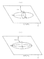
この2種類の位相層について図8を用いて説明すると、図示のように層面Sの法線方向にz軸、層面S内の直交方向をx軸とy軸をとり、x軸方向、y軸方向、z軸方向の屈折率をそれぞれnx 、ny 、nz とし、図8(a)に示すように、nx >ny =nz の関係にある位相層が層面S内に光学的に正の一軸性を有する位相層であり、以下の説明では正のAプレートと称することにする。また、図8(b)に示すように、nx =ny >nz の関係にある位相層が層面Sの法線方向に光学的に負の一軸性を有する位相層であり、以下の説明では負のCプレートと称することにする。
【0027】
このような正のAプレートは、例えば、正の屈折率異方性を持つネマテック重合性液晶分子を層面内にプラナー配向させることにより構成することができ、負のCプレートはそのような液晶にカイラル剤を混合して螺旋軸が層面の法線方向を向くようにツイストさせることにより構成することができる。
【0028】
ところで、電圧が印加されない状態では液晶セル中の液晶分子が基板に略垂直に立つように配向していて黒表示になり、電圧が印加された状態では液晶分子が基板に略平行に配向していて白表示になる垂直配向(VA)モードのLCDにおいては、従来、特許文献2に開示されているように、液晶セルと一方の偏光板の間に、偏光板側に正のAプレートを、液晶セル側に負のCプレートを配置して、斜め方向から観察した際の黒表示画素の光漏れを低減させている。このような構成では、前記したように、偏光板及び液晶セルの基板に対して正のAプレートと負のCプレートを屈折率差のある粘着剤により貼り合わせなけれならないため、界面で光の反射が生じ表示のコントラストが低下する等の問題がある。
【0029】
そこで、本発明においては、図1(a)、(b)、(c)に本発明による液晶ディスプレイの液晶セル部分の模式的断面図を示すように、液晶セルを構成する透明基板1、1’の内側(液晶セル内)に正のAプレートaと負のCプレートcとを透明基板1、1’(図では、透明基板1)に積層して配置する。なお、図1中、符号2は透明基板1、1’間をシールして液晶セルを構成するシール部材、符号3はVAモードの液晶層、符号4はRGBのカラーフィルター(赤色を透過するフィルターを“R”、緑色を透過するフィルターを“G”、青色を透過するフィルターを“B”で表記してある。)を示す。また、図1中では、液晶層3を配向する配向層、電極層、各画素を制御するTFT等の図示は省いてある。
【0030】
図1(a)は、カラーフィルターを設けない白黒表示の液晶セルであり、図1(b)、(c)は、カラーフィルター3を設けたカラー表示の液晶セルである。カラー表示液晶セルの場合、図1(b)に示すように、まず、カラーフィルター3を積層し、その上に正のAプレートaや負のCプレートcを積層してもよいが、図1(c)に示すように、透明基板1、1’にまず正のAプレートaや負のCプレートcを積層し、その上にカラーフィルター3を積層する方が望ましい。その理由は、正のAプレートa、負のCプレートc等の位相差制御層には波長分散が伴うため、R、G、Bの波長毎に最適な厚さが異なる。具体的には、同じ材料を用いると、R領域の厚さ>G領域の厚さ>B領域の厚さの順となる。そのため、正のAプレートaと負のCプレートは、図1(c)に示すように、R、G、Bの画素毎にパターニングして作製することが望ましく、そうすると、画素間に段差が生じてしまう。このような画素間の段差を補償して液晶層3の厚さを均一にするためには、カラーフィルター3のR、G、Bの要素に異なる厚さを持たせることができる図1(c)の配置が望ましい。なお、図1(b)のような配置の場合には、このような画素間の段差はCプレートc上に保護層を設け、その保護層の厚さを画素間で異ならせて補償するようにすることが望ましい。
【0031】
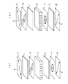
図2(a)、(b)〜図4(a)、(b)に、本発明に基づいて正のAプレートaと負のCプレートcの少なくとも一方を液晶セル内に配置する場合の液晶ディスプレイの可能な構成を模式的に示す分解斜視図であり、これらの図では、シール部材、配向層、電極層、TFT等の図示は省いてある。また、これらの図において、正のAプレートa、負のCプレートcは、図示上分離して示してあるが、実際には、基板1、1’に対して配向膜を介して直接積層されている(図1(b)のように、カラーフィルター3を介する場合もある。)。なお、図4(a)、(b)のように、正のAプレートaと負のCプレートcの中の一方のみを液晶セル内に配置するように構成してもよい。
【0032】
図2(a)、(b)〜図4(a)、(b)の場合を簡単に説明する。図中、2枚の透明基板1、1’とその間に配置された液晶層3とからなる液晶セルの両側に、吸収軸6が相互に直交して直交ニコル状態の2枚の偏光板5、5’が配置されて液晶ディスプレイが構成されている。
【0033】
図2(a)の場合は、透明基板1の内側に偏光板5側に正のAプレートaが、液晶層3側に負のCプレートcが、透明基板1の内側に順に積層されている。
【0034】
図2(b)の場合は、透明基板1の内側に負のCプレートcが、透明基板1’の内側に正のAプレートaが分離されてそれぞれ透明基板1、1’の内側に積層されている。
【0035】
図3(a)の場合は、図2(b)の場合と逆で、透明基板1の内側に正のAプレートaが、透明基板1’の内側に負のCプレートcが分離されてそれぞれ透明基板1、1’の内側に積層されている。
【0036】
図3(b)の場合は、図2(a)の場合と逆で、透明基板1’の内側に偏光板5’側に正のAプレートaが、液晶層3側に負のCプレートcが順に積層されている。
【0037】
図4(a)の場合は、透明基板1の内側に正のAプレートaが積層されており、負のCプレートcは透明基板1’の外側に積層されている。
【0038】
図4(b)の場合は、透明基板1’の内側に負のCプレートcが積層されており、正のAプレートaは透明基板1の外側に積層されている。
【0039】
なお、何れの場合も、偏光板5、5’に隣接する正のAプレートaの光学軸は偏光板5、5’の吸収軸6と直交するような位置関係で配置される。
【0040】
以上の本発明の構成においては、従来液晶セルの外側に貼り合わせて用いられる位相差制御層(正のAプレートa、負のCプレートc)の全部あるいは一部を、図2(a)、(b)〜図4(a)、(b)に示すように、重合性液晶分子を用いて液晶セル内に設けるため、界面反射光が少なく高コントラストで視野角度の広いVAモードのLCDを提供することができる。なお、図4(a)、(b)のように、正のAプレートa又は負のCプレートcの一方のみを液晶セル外に配置する場合も、透明基板1、1’の外側に直接重合性液晶分子を用いて設けることができるため、同様に界面反射光が少なく高コントラストで視野角度の広いVAモードのLCDを提供することができる。なお、透明基板1、1’の外側に配置する正のAプレートa、負のCプレートcは、直接重合性液晶分子を用いて設ける代わりに、従来のように、ポリカーボネート等の透明高分子フィルムを1軸又は2軸延伸処理して作製したフィルム状態のものを用いてもよい。この場合は、透明基板1、1’の外側に粘着剤を用いて貼り付ける。
【0041】
ところで、本発明において正のAプレートa及び負のCプレートcとして用いる位相差制御層を構成する三次元架橋が可能な液晶モノマー分子(重合性液晶分子)としては、例えば特許文献3や特許文献4で開示されているような液晶性モノマー及びそれとキラル化合物の混合物がある。このような重合性液晶材料の一例としては、次の〔化11〕に包含されるような化合物や、下記の〔化1〕〜〔化10〕の化合物の2種類以上を混合して使用することができる。なお、一般化学式〔化11〕で示される液晶性モノマーの場合、Xは2〜5(整数)であることが好ましい。
【0042】
また、カイラル剤としては、例えば一般化学式〔化12〕〜〔化14〕に示されるようなカイラル剤を用いることができる。なお、一般化学式〔化12〕、〔化13〕で示されるカイラル剤の場合、Xは2〜12(整数)であることが望ましく、また、一般化学式〔化14〕で示されるカイラル剤の場合、Xが2〜5(整数)であることが望ましい。
【0043】
【化1】

【化2】
【化3】
【化4】
【化5】
【化6】
【化7】
【化8】
【化9】
【化10】
【化11】
【化12】
【化13】
【化14】
【0057】
(1)下地基板の準備
適当な洗浄処理を施した基板としてのガラス基板(1737材、コーニング社製)上に、配向膜材料としてAL1254(JSR製)を用い、フレキソ印刷により配向膜を形成した。
【0058】
次に、当該配向膜を既知の手法によりラビング処理して下地基板を得た。本実施例においては、基板としてガラス基板を用いているが、本発明はガラス基板にのみ限定されるものではなく、ポリカーボネート、ポリメチルメタクリレート、ポリエチレンテレフタレート、トリアセチルセルロース等からなるプラスチック基板であってもよいし、またさらに、ポリエーテルスルホン、ポリスルホン、ポリプロプレン、ポリイミド、ポリアミドイミド、ポリエーテルケトン等のフィルムを用いることもできる。
【0059】
(2)インキの調整
正のAプレート位相差制御層用インキとして、両端に重合可能なアクリレート基を有すると共に、中央部のメソゲンと上記アクリレートの間にスペーサを有する液晶材料を75重両部、光重合開始材としてイルガキュアIrg184(Chiba Speciality Chemicals製)を1重量部、溶剤としてのトルエン25重量部を混合して、重合性液晶インキを製作した。
【0060】
負のCプレート位相差制御層用重合性液晶材料としては、上記Aプレート用位相差制御層インキに、カイラル材として両末端に重合可能なアクリレート基を有するカイラル剤を5重量部加えて製作した。
【0061】
(3)正のAプレート位相差制御層の形成
調整した上記インキを、スピンコーティング法を用いて(1)で配向膜を形成した基板上に塗布した。なお、本実施例ではスピンコーティング法を適用したが、基板上に均一に塗布が可能であればこれに限られる訳ではなく、ダイコーティング、スリットコーティング、及び、これらを組み合わせた手法であってもよく、特に限定されない。
【0062】
続いて、当該基板をホットプレート上で100℃、5分間加熱し、残存溶剤を除去し、液晶構造を発現させた。
【0063】
続いて、フォトマスクを介して塗布した液晶膜に紫外線照射を行い(10J/cm2 、波長365nm)、後の工程で緑の画素が形成される部分にのみパターンを焼き付けた。
【0064】
その後、現像液としてのメタノールに3分間浸漬して未露光部分の液晶膜を除去し、純水にて1分間リンスした後、100℃のホットプレート上で10分間加熱して完全に乾燥させて、正のAプレート位相差制御層を1.0μm厚で得た。
【0065】
同様な手法を用い、膜厚を変化させつつ、青、赤の画素についても塗布、パターニングを行った。膜厚はそれぞれ0.8m、1.2mとした。
【0066】
(4)負のCプレート位相差制御層の形成
上記(1)〜(3)で製作した基板上に、負のCプレート位相差制御層インキを用い、正のAプレート位相差制御層と同様な手法により、負のCプレート位相差制御層を2.5μmの厚さでパターニングして、正のAプレート位相差制御層上に積層構成した。本実施例では、正のAプレート位相差制御層上に直接負のCプレート位相差制御層を積層したが、図2〜図4に示すように、正のAプレート位相差制御層と負のCプレート位相差制御層は、それぞれバックライト側及び観察側の何れの基板の内側あるいは外側に構成してもよく、図2(a)、(b)〜図4(a)、(b)に示す構成であれば特に限定されない。
【0067】
上記の手法を繰り返し、膜厚をそれぞれ2.6m、2.4mと変化させつつ、青、赤の画素についても同様の塗布、パターニングを行った。
【0068】
(5)カラーフィルターの形成
上記の正のAプレート位相差制御層、負のCプレート位相差制御層の各位相差制御層が積層された基板上に、カラーフィルターとしてのブラックマトリクス、各RGB着色画素パターンを、既知の手法を用いて作成した。その際、図1(c)に示すように、RGB着色画素パターンは、R、G、Bの要素で異なる厚さを持つようにして、画素間の段差を補償してVAモードの液晶層の厚さが均一になるようにした。
【0069】
次に、電極としてITO膜をスパッタリングの手法により2000Å厚に形成した後、液晶分子の配向方向を制御する突起を、その配向方向が4分割でかつ配向分割面積が等しくなるよう設けた。
【0070】
本実施例では、カラーフィルター層を位相差制御層の上に設けているが、本発明においてはこの位置に限定されるものではなく、2枚の対向するガラス基板の内側であればよく、特に限定されない。
【0071】
(6)垂直配向ディスプレイの構成
上記(1)〜(5)で得られた位相差制御機能付きMVAモードLCD用カラーフィルターを用い、その上に垂直配向用の配向膜を製膜後、対向基板と間隙を設けて貼り合わせ、負の誘電異方性を持つ液晶MLC−6608(メルク社製)を注入して、MVAモード液晶ディスプレイを得た。
【0072】
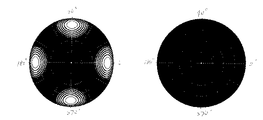
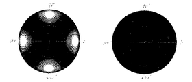
得られたMVAモード液晶ディスプレイの黒表示時の光漏れを、比較対照例として位相差制御層を設けなかった場合と合わせて、図5〜図7に示す。各図中、左側が比較対照例、右側が本実施例の光漏れを示す。測定には、EZContrasut160R (ELDIM製)を用いた。図5の場合は、B(青色)として450nm、図6の場合は、G(緑色)として550nm、図7の場合は、R(赤色)として610nmの光源を用い、それぞれ構成した液晶ディスプレイの黒状態に入射させ、その際の光漏れを方位角度360°、極角度80°の範囲で検証した。2枚の偏光板の吸収軸の方位角度は45°と135°である。なお、図5〜図7の各図において、円の中心が極角度0°、円の周が極角度80°である。それぞれの波長で、本実施例の場合は、位相差制御層なしの場合に比べて、方位角度0°、90°、180°、270°における光漏れが大幅に低減されていることが分かる。
【0073】
なお、本発明においては、配向膜層、位相差制御層はそれぞれ有効表示エリアのみにパターニングされて設けることができ、対向基板と張り合わせる際にシール部材2(図1)が設けられる部分はガラス表面であるため、確実なシールが可能であり、耐久性に優れた液晶ディスプレイを構成することが可能である。なお、この場合に、位相差制御層のパターニングされた最外端面は、シール部材2の糊付着部(シール部)から50μm以上内側にパターニングして形成することが望ましい。
【0074】
また、本発明において、重合性液晶分子を配向させるためには、配向膜が必要である。特に、1層目の正のAプレートa又は負のCプレートcの位相差制御層を基板上に設ける際には配向膜が必須となる。正のAプレートa上に負のCプレートcを積層する場合には、下地の正のAプレートaの配向が配向膜として機能させることも可能であるが、より確実な配向を得るためには、2層目のための配向膜を設けることが望ましい。
【0075】
なお、本発明において、VAモードのLCDにおいける液晶層3に用いる液晶分子の屈折率異方性(異常光屈折率から常光屈折率を引いた値)は一般に0.05から0.30の範囲にあり、正のAプレートa、負のCプレートcの位相差制御層として用いる重合性液晶分子の屈折率異方性は一般に0.05から0.30の範囲にあり、液晶セルのセルギャップ(液晶層3の厚さ)は一般に1.0μmから6.0μmであり、かつ、重合性液晶分子からなる正のAプレートa、負のCプレートcの膜厚は0.1μmから10.0μmである。
【0076】
以上、本発明の位相差制御機能を有する液晶ディスプレイ用基板及びそれを用いた液晶ディスプレイをその原理と実施例に基づいて説明してきたが、本発明はこれら実施例に限定されず種々の変形が可能である。
【0077】
【発明の効果】
以上の説明から明らかなように、本発明の位相差制御機能を有する液晶ディスプレイ用基板及びそれを用いた液晶ディスプレイにおいては、液晶ディスプレイの液晶層を挟む透明基板の液晶層側に、重合性液晶分子からなる層面内に光軸を有する正の一軸性位相層、若しくは、重合性液晶分子からなる層面の法線方向に光軸を有する負の一軸性位相層の中、少なくとも一方がパターニングされて設けられているので、視野角度を拡大するために通常フィルム状態として液晶セル外に貼り付けられる位相差板を、液晶セルを構成する透明基板に直接パターニングし、かつ、液晶セル内部に包含させることにより、接着剤の界面反射によるコントラストの低下を防ぎ、波長分散の少ない高品位な液晶ディスプレイ、特に垂直配向モードの液晶ディスプレイを構成することが可能となる。
【図面の簡単な説明】
【図1】本発明による液晶ディスプレイの液晶セル部分の模式的断面図である。
【図2】本発明に基づいて正のAプレートと負のCプレートの少なくとも一方を液晶セル内に配置する場合の液晶ディスプレイの可能な構成を模式的に示す分解斜視図である。
【図3】本発明に基づいて正のAプレートと負のCプレートの少なくとも一方を液晶セル内に配置する場合の液晶ディスプレイの可能な構成を模式的に示す分解斜視図である。
【図4】本発明に基づいて正のAプレートと負のCプレートの少なくとも一方を液晶セル内に配置する場合の液晶ディスプレイの可能な構成を模式的に示す分解斜視図である。
【図5】本発明の1実施例による位相差制御機能付きMVAモードLCD用カラーフィルターを用いたMVAモード液晶ディスプレイの黒表示時のB光の光漏れを比較対照例と合わせて示す図である。
【図6】本発明の1実施例による位相差制御機能付きMVAモードLCD用カラーフィルターを用いたMVAモード液晶ディスプレイの黒表示時のG光の光漏れを比較対照例と合わせて示す図である。
【図7】本発明の1実施例による位相差制御機能付きMVAモードLCD用カラーフィルターを用いたMVAモード液晶ディスプレイの黒表示時のR光の光漏れを比較対照例と合わせて示す図である。
【図8】層面内に光軸を有する正の一軸性位相層と層面の法線方向に光軸を有する負の一軸性位相層とを説明するための図である。
【符号の説明】
S…層面
a…正のAプレート
c…負のCプレート
1、1’…透明基板
2…シール部材
3…VAモードの液晶層
4…RGBのカラーフィルター
5、5’…偏光板
6…吸収軸[0001]
TECHNICAL FIELD OF THE INVENTION
The present invention relates to a liquid crystal display substrate having a phase difference control function and a liquid crystal display using the same, and more particularly, to a liquid crystal display substrate having a phase difference control layer patterned inside a liquid crystal cell and a liquid crystal display using the same. Things.
[0002]
[Prior art]
2. Description of the Related Art The market for color liquid crystal displays (hereinafter, liquid crystal displays are referred to as LCDs) has been rapidly expanding, mainly for notebook computers, due to its features of thinness, light weight, low power consumption, and flickerlessness. Recently, as a part of such a display for a PC, there is a demand for a monitor for a desktop that is larger than a notebook personal computer. LCDs have been used not only for PCs but also for TVs where CRTs have been the mainstream in the past.
[0003]
Here, as a problem of the LCD, there is a problem of its narrow viewing angle. This is because, when the LCD is viewed from an oblique direction, light leaks from a pixel that should originally display black, and this causes the contrast to be inverted, preventing correct display. In view of such a problem, as described in
[0004]
[Patent Document 1]
JP-A-10-153802
[0005]
[Patent Document 2]
JP-A-11-258605
[0006]
[Patent Document 3]
JP-A-7-258638
[0007]
[Patent Document 4]
Japanese Patent Publication No. Hei 10-508882
[0008]
[Problems to be solved by the invention]
These retardation films are usually used by laminating a polarizing plate and an optical axis (an absorption axis in the case of a polarizing plate and an optical axis in the case of a retardation film) so as to form a specific angle. However, the pressure-sensitive adhesive used at that time has a smaller refractive index than that of a polarizing plate or a retardation film (retardation film), so that light is reflected at the interface, and the display contrast is reduced. was there.
[0009]
In general, since phase difference compensation involves chromatic dispersion, compensation is performed around a specific wavelength. In many cases, phase difference compensation is designed around green having the highest visibility. As a result, the black display pixel cannot be displayed in a completely black state, and the red and blue light components leak, resulting in a purple-black display.
[0010]
In addition, since the retardation film changes its volume by absorbing moisture, the retardation changes, and when applied to an LCD, there is a disadvantage that the screen is distorted. This tendency becomes more conspicuous as the area of the retardation film increases, and is particularly problematic in liquid crystal TVs that have recently been applied.
[0011]
The present invention has been made in view of such problems of the prior art, and an object of the present invention is to arrange a phase difference control layer, which is usually used in a film state, directly on a liquid crystal layer side of a substrate constituting an LCD. Another object of the present invention is to cancel the interfacial reflection caused by the adhesive, thereby enabling a high-contrast display.
[0012]
It is another object of the present invention to provide an in-cell structure that can be directly laminated on a substrate such as a transparent substrate or a color filter so as to prevent a change in volume due to moisture absorption as seen in a conventional retardation film.
[0013]
Further, in the present invention, the phase difference control layer is patterned into regions corresponding to R (red), G (green), and B (blue), so that the phase difference is separately set in the pixel region of each color. To enable phase difference compensation without chromatic dispersion.
[0014]
[Means for Solving the Problems]
The liquid crystal display substrate having a phase difference control function of the present invention that achieves the above object has a transparent substrate sandwiching a liquid crystal layer of a liquid crystal display, and the liquid crystal layer side has an optical axis in a layer plane composed of polymerizable liquid crystal molecules. At least one of a positive uniaxial phase layer or a negative uniaxial phase layer having an optical axis in a direction normal to a layer surface composed of polymerizable liquid crystal molecules is provided by being patterned. It is.
[0015]
In this case, it is desirable that the negative uniaxial phase layer having an optical axis in the direction normal to the layer surface composed of polymerizable liquid crystal molecules is composed of a mixture of polymerizable liquid crystal molecules and a chiral agent.
[0016]
Another substrate for a liquid crystal display having a phase difference control function of the present invention is a transparent substrate sandwiching a liquid crystal layer of a liquid crystal display, the liquid crystal layer being provided with an alignment film and an optical axis in a layer plane composed of polymerizable liquid crystal molecules. And a negative uniaxial phase layer having an optical axis in a direction normal to a layer surface composed of polymerizable liquid crystal molecules.
[0017]
In this case, between the positive uniaxial phase layer having an optical axis in the layer plane composed of polymerizable liquid crystal molecules and the negative uniaxial phase layer having an optical axis in the direction normal to the layer plane composed of polymerizable liquid crystal molecules. It is desirable to have an alignment film.
[0018]
In the liquid crystal display substrate having the first phase difference control function, a positive uniaxial phase layer having an optical axis in a layer plane or a negative uniaxial phase layer having an optical axis in a direction normal to the layer plane is used. It is also possible for one to be attached to the other side of the liquid crystal layer of the liquid crystal display in a film state on the side opposite to the liquid crystal layer of the transparent substrate.
[0019]
Above, a phase layer having an optically positive uniaxial property in the layer plane composed of polymerizable liquid crystal molecules, or a phase layer having an optically negative uniaxial property in the normal direction of the layer plane composed of polymerizable liquid crystal molecules. Among them, a substrate for a liquid crystal display having a phase difference control function in which at least one is patterned has regions of R, G, and B colors, and at least one of the phase difference layers has the R, G, or B region. It is desirable to be formed by patterning in accordance with the B3 color region.
[0020]
In the above description, it is desirable that the alignment mode of the liquid crystal layer is the vertical alignment mode.
[0021]
In this case, the liquid crystal molecules used for the liquid crystal layer in the vertical alignment mode have a refractive index anisotropy of 0.05 to 0.30, and the polymerizable liquid crystal molecules used for the phase layer have a refractive index anisotropy of 0. It is generally from 0.05 to 0.30, and the thickness of the liquid crystal layer in the vertical alignment mode is from 1.0 μm to 6.0 μm, and the film of the phase layer made of polymerizable liquid crystal molecules. The thickness is generally between 0.1 μm and 10.0 μm.
[0022]
The present invention includes a liquid crystal display using a liquid crystal display substrate having the above-described phase difference control function.
[0023]
According to the present invention, a positive uniaxial phase layer having an optical axis composed of polymerizable liquid crystal molecules or a normal direction of a layer surface composed of polymerizable liquid crystal molecules is provided on a liquid crystal layer side of a transparent substrate sandwiching a liquid crystal layer of a liquid crystal display. Since at least one of the negative uniaxial phase layers having an optical axis is provided by being patterned, a retardation plate that is attached to the outside of the liquid crystal cell in a normal film state in order to expand the viewing angle is provided by a liquid crystal. By patterning directly on the transparent substrate that constitutes the cell and including it inside the liquid crystal cell, it prevents contrast deterioration due to interfacial reflection of the adhesive and reduces the wavelength dispersion of high-quality liquid crystal displays, especially vertical alignment mode liquid crystals. A display can be configured.
[0024]
BEST MODE FOR CARRYING OUT THE INVENTION
The basic principle of the phase difference compensation used in the present invention is known, for example, from
[0025]
First, the phase difference control layer will be described. As the retardation control layer used in the present invention, a positive uniaxial phase layer having an optical axis in a layer plane and a negative uniaxial phase layer having an optical axis in a direction normal to the layer plane are used.
[0026]
The two types of phase layers will be described with reference to FIG. 8. As shown in the drawing, the z axis is taken in the direction normal to the layer surface S, the x axis and the y axis are taken in the direction perpendicular to the layer surface S, and the x axis direction and the y axis are taken. In the direction and the z-axis direction, respectively. x , N y , N z Then, as shown in FIG. x > N y = N z Is a phase layer having optically positive uniaxiality in the layer surface S, and will be referred to as a positive A plate in the following description. Also, as shown in FIG. x = N y > N z Is a phase layer having optically negative uniaxiality in the normal direction of the layer surface S, and will be referred to as a negative C plate in the following description.
[0027]
Such a positive A plate can be constituted by, for example, aligning a nematic polymerizable liquid crystal molecule having a positive refractive index anisotropy in a plane plane with a negative C plate. It can be constituted by mixing a chiral agent and twisting the helical axis so that the helical axis is directed to the normal direction of the layer surface.
[0028]
By the way, in the state where no voltage is applied, the liquid crystal molecules in the liquid crystal cell are oriented so as to stand substantially perpendicular to the substrate, resulting in black display, and in the state where the voltage is applied, the liquid crystal molecules are oriented substantially parallel to the substrate. Conventionally, in a vertical alignment (VA) mode LCD in which a white display is provided, a positive A plate is provided between the liquid crystal cell and one polarizing plate on the polarizing plate side, as disclosed in
[0029]
Therefore, in the present invention, as shown in FIGS. 1A, 1B and 1C, a schematic sectional view of a liquid crystal cell portion of a liquid crystal display according to the present invention is shown. A positive A plate a and a negative C plate c are laminated on the
[0030]
FIG. 1A shows a liquid crystal cell for monochrome display without a color filter, and FIGS. 1B and 1C show liquid crystal cells for color display with a
[0031]
FIGS. 2 (a) and 2 (b) to 4 (a) and 4 (b) show a liquid crystal in which at least one of a positive A plate a and a negative C plate c is arranged in a liquid crystal cell according to the present invention. FIG. 3 is an exploded perspective view schematically showing a possible configuration of a display, in which illustration of a sealing member, an alignment layer, an electrode layer, a TFT, and the like is omitted. In these figures, the positive A plate a and the negative C plate c are shown separately from each other in the drawing, but are actually stacked directly on the
[0032]
The cases of FIGS. 2A and 2B to FIGS. 4A and 4B will be briefly described. In the figure, on both sides of a liquid crystal cell composed of two
[0033]
In the case of FIG. 2A, a positive A plate a is disposed on the
[0034]
In the case of FIG. 2 (b), a negative C plate c is separated inside the
[0035]
In the case of FIG. 3A, the positive A plate a is separated inside the
[0036]
In the case of FIG. 3 (b), contrary to the case of FIG. 2 (a), a positive A plate a is provided on the polarizing plate 5 'side inside the transparent substrate 1' and a negative C plate c is provided on the
[0037]
In the case of FIG. 4A, the positive A plate a is laminated inside the
[0038]
In the case of FIG. 4B, the negative C plate c is laminated inside the
[0039]
In any case, the optical axis of the positive A plate a adjacent to the
[0040]
In the configuration of the present invention described above, all or a part of the phase difference control layers (positive A-plate a and negative C-plate c) conventionally used by being bonded to the outside of the liquid crystal cell are shown in FIG. (B) As shown in FIGS. 4 (a) and 4 (b), the liquid crystal cell is provided in the liquid crystal cell using polymerizable liquid crystal molecules. can do. In addition, as shown in FIGS. 4A and 4B, when only one of the positive A plate a and the negative C plate c is disposed outside the liquid crystal cell, the direct polymerization is performed on the outside of the
[0041]
Incidentally, as liquid crystal monomer molecules (polymerizable liquid crystal molecules) capable of three-dimensional cross-linking constituting the retardation control layer used as the positive A plate a and the negative C plate c in the present invention, for example,
[0042]
Further, as the chiral agent, for example, a chiral agent represented by a general chemical formula [Chemical Formula 12] to [Chemical Formula 14] can be used. In the case of the chiral agent represented by the general chemical formulas [Chemical Formula 12] and [Formula 13], X is preferably 2 to 12 (integer). , X are preferably 2 to 5 (integer).
[0043]
Embedded image
Embedded image
Embedded image
Embedded image
Embedded image
Embedded image
Embedded image
Embedded image
Embedded image
Embedded image
Embedded image
Embedded image
Embedded image
Embedded image
[0057]
(1) Preparation of base substrate
An alignment film was formed by flexographic printing using AL1254 (manufactured by JSR) as an alignment film material on a glass substrate (1737 material, manufactured by Corning Incorporated) as a substrate having been subjected to an appropriate cleaning treatment.
[0058]
Next, the alignment film was rubbed by a known method to obtain a base substrate. In the present embodiment, a glass substrate is used as the substrate, but the present invention is not limited to the glass substrate alone, and is a plastic substrate made of polycarbonate, polymethyl methacrylate, polyethylene terephthalate, triacetyl cellulose, or the like. Alternatively, a film of polyethersulfone, polysulfone, polypropylene, polyimide, polyamideimide, polyetherketone, or the like may be used.
[0059]
(2) Ink adjustment
As a positive A-plate retardation control layer ink, a liquid crystal material having polymerizable acrylate groups at both ends and a spacer between the mesogen in the center and the acrylate is used in 75 parts, and Irgacure is used as a photopolymerization initiator. 1 part by weight of Irg184 (manufactured by Chiba Specialty Chemicals) and 25 parts by weight of toluene as a solvent were mixed to prepare a polymerizable liquid crystal ink.
[0060]
The polymerizable liquid crystal material for the negative C-plate retardation control layer was manufactured by adding 5 parts by weight of a chiral agent having a polymerizable acrylate group at both ends as a chiral material to the ink for the A-plate retardation control layer. .
[0061]
(3) Formation of positive A-plate retardation control layer
The adjusted ink was applied on the substrate on which the alignment film was formed in (1) by using a spin coating method. In this example, the spin coating method was applied, but the present invention is not limited to this as long as it can be applied uniformly on the substrate.Die coating, slit coating, and a method combining these are also possible. Well, there is no particular limitation.
[0062]
Subsequently, the substrate was heated on a hot plate at 100 ° C. for 5 minutes to remove the residual solvent, thereby developing a liquid crystal structure.
[0063]
Subsequently, the applied liquid crystal film was irradiated with ultraviolet light through a photomask (10 J / cm 2). 2 , Wavelength 365 nm), and a pattern was printed only on a portion where a green pixel is formed in a later step.
[0064]
Thereafter, the liquid crystal film in the unexposed portion was removed by immersion in methanol as a developer for 3 minutes, rinsed with pure water for 1 minute, and then heated on a hot plate at 100 ° C. for 10 minutes to be completely dried. And a positive A-plate retardation control layer having a thickness of 1.0 μm.
[0065]
Using the same technique, application and patterning were performed on blue and red pixels while changing the film thickness. The film thickness was 0.8 m and 1.2 m, respectively.
[0066]
(4) Formation of negative C-plate retardation control layer
The negative C-plate phase difference control layer is formed on the substrate manufactured in the above (1) to (3) by using the negative C-plate phase difference control layer ink in the same manner as the positive A-plate phase difference control layer. It was patterned with a thickness of 2.5 μm and laminated on the positive A-plate phase difference control layer. In the present embodiment, the negative C-plate phase difference control layer is directly laminated on the positive A-plate phase difference control layer. However, as shown in FIGS. The C-plate retardation control layer may be formed inside or outside any of the substrates on the backlight side and the observation side, respectively, as shown in FIGS. 2 (a), (b) to 4 (a), (b). There is no particular limitation as long as the configuration is as shown.
[0067]
The above method was repeated, and the same coating and patterning were performed on the blue and red pixels while changing the film thickness to 2.6 m and 2.4 m, respectively.
[0068]
(5) Formation of color filter
A black matrix as a color filter and each of the RGB colored pixel patterns are formed on a substrate on which the respective phase difference control layers of the positive A plate phase difference control layer and the negative C plate phase difference control layer are laminated by a known method. Created using At this time, as shown in FIG. 1 (c), the RGB colored pixel patterns are made to have different thicknesses for the R, G, and B elements to compensate for the step between the pixels and to form the VA mode liquid crystal layer. The thickness was made uniform.
[0069]
Next, after an ITO film was formed as an electrode to a thickness of 2000 mm by a sputtering technique, projections for controlling the alignment direction of liquid crystal molecules were provided so that the alignment direction was divided into four and the alignment division areas were equal.
[0070]
In the present embodiment, the color filter layer is provided on the retardation control layer. However, the present invention is not limited to this position, and it is sufficient that the color filter layer is inside two opposing glass substrates. Not limited.
[0071]
(6) Configuration of vertical alignment display
Using the color filter for MVA mode LCD with a phase difference control function obtained in the above (1) to (5), forming an alignment film for vertical alignment thereon, and bonding the same to a counter substrate with a gap provided, Liquid crystal MLC-6608 (manufactured by Merck) having a negative dielectric anisotropy was injected to obtain an MVA mode liquid crystal display.
[0072]
Light leakage at the time of black display of the obtained MVA mode liquid crystal display is shown in FIGS. 5 to 7 together with a case where no phase difference control layer is provided as a comparative example. In each figure, the left side shows the comparative example, and the right side shows the light leakage of this example. For the measurement, EZContrasut160R (manufactured by ELDIM) was used. In the case of FIG. 5, a light source of 450 nm is used as B (blue), in FIG. 6, a light source of 550 nm is used as G (green), and in FIG. 7, a light source of 610 nm is used as R (red). Then, the light leakage at that time was verified in the range of the azimuth angle of 360 ° and the polar angle of 80 °. The azimuthal angles of the absorption axes of the two polarizing plates are 45 ° and 135 °. In each of FIGS. 5 to 7, the center of the circle has a polar angle of 0 ° and the circumference of the circle has a polar angle of 80 °. It can be seen that the light leakage at the azimuth angles of 0 °, 90 °, 180 °, and 270 ° is significantly reduced in the case of the present embodiment at each wavelength as compared with the case without the phase difference control layer.
[0073]
In the present invention, the alignment film layer and the phase difference control layer can be provided by being patterned only in the effective display area, and the portion where the sealing member 2 (FIG. 1) is provided when bonding with the counter substrate is made of glass. Since it is a surface, a reliable seal is possible and a liquid crystal display having excellent durability can be formed. In this case, it is desirable that the patterned outermost end surface of the phase difference control layer is formed by patterning 50 μm or more inward from the glue adhering portion (seal portion) of the
[0074]
In the present invention, an alignment film is required to align the polymerizable liquid crystal molecules. In particular, when the first phase difference control layer of the positive A plate a or the negative C plate c is provided on the substrate, an alignment film is essential. When the negative C plate c is laminated on the positive A plate a, the orientation of the underlying positive A plate a can be made to function as an orientation film, but in order to obtain a more reliable orientation, It is desirable to provide an alignment film for the second layer.
[0075]
In the present invention, the refractive index anisotropy (value obtained by subtracting the ordinary light refractive index from the extraordinary light refractive index) of the liquid crystal molecules used for the
[0076]
As described above, the liquid crystal display substrate having a phase difference control function and the liquid crystal display using the same according to the present invention have been described based on the principle and the embodiments. However, the present invention is not limited to these embodiments, and various modifications may be made. It is possible.
[0077]
【The invention's effect】
As is clear from the above description, in the liquid crystal display substrate having a phase difference control function of the present invention and the liquid crystal display using the same, the polymerizable liquid crystal is provided on the liquid crystal layer side of the transparent substrate sandwiching the liquid crystal layer of the liquid crystal display. At least one of a positive uniaxial phase layer having an optical axis in a layer surface composed of molecules, or a negative uniaxial phase layer having an optical axis in a direction normal to the layer surface composed of polymerizable liquid crystal molecules, is patterned. Since it is provided, a retardation plate that is normally attached to the outside of the liquid crystal cell in a film state to expand the viewing angle is directly patterned on a transparent substrate constituting the liquid crystal cell, and included in the liquid crystal cell. This prevents contrast deterioration due to interfacial reflection of the adhesive and prevents high-quality liquid crystal displays with low wavelength dispersion, especially vertical alignment mode liquid crystal displays. It is possible to configure the play.
[Brief description of the drawings]
FIG. 1 is a schematic sectional view of a liquid crystal cell portion of a liquid crystal display according to the present invention.
FIG. 2 is an exploded perspective view schematically showing a possible configuration of a liquid crystal display when at least one of a positive A plate and a negative C plate is arranged in a liquid crystal cell according to the present invention.
FIG. 3 is an exploded perspective view schematically showing a possible configuration of a liquid crystal display when at least one of a positive A plate and a negative C plate is disposed in a liquid crystal cell according to the present invention.
FIG. 4 is an exploded perspective view schematically showing a possible configuration of a liquid crystal display when at least one of a positive A plate and a negative C plate is arranged in a liquid crystal cell according to the present invention.
FIG. 5 is a diagram showing light leakage of B light during black display of an MVA mode liquid crystal display using a color filter for an MVA mode LCD with a phase difference control function according to one embodiment of the present invention, together with a comparative example. .
FIG. 6 is a diagram showing light leakage of G light during black display of an MVA mode liquid crystal display using a color filter for an MVA mode LCD with a phase difference control function according to one embodiment of the present invention, together with a comparative example. .
FIG. 7 is a diagram showing light leakage of R light during black display of an MVA mode liquid crystal display using a color filter for an MVA mode LCD with a phase difference control function according to one embodiment of the present invention, together with a comparative example. .
FIG. 8 is a diagram for explaining a positive uniaxial phase layer having an optical axis in a layer plane and a negative uniaxial phase layer having an optical axis in a direction normal to the layer plane.
[Explanation of symbols]
S ... layer surface
a ... Positive A plate
c ... Negative C plate
1, 1 '... transparent substrate
2. Seal member
3. VA mode liquid crystal layer
4: RGB color filter
5, 5 '... polarizing plate
6 ... Absorption axis
Claims (20)
Priority Applications (3)
| Application Number | Priority Date | Filing Date | Title |
|---|---|---|---|
| JP2003028176A JP4329983B2 (en) | 2003-02-05 | 2003-02-05 | Liquid crystal display |
| US10/771,445 US20040156001A1 (en) | 2003-02-05 | 2004-02-05 | Liquid crystal display-specific substrate having a phase difference control function, and liquid crystal display using the same |
| US11/362,802 US7495729B2 (en) | 2003-02-05 | 2006-02-28 | Liquid crystal display-specific substrate having a phase difference control function, and liquid crystal display using the same |
Applications Claiming Priority (1)
| Application Number | Priority Date | Filing Date | Title |
|---|---|---|---|
| JP2003028176A JP4329983B2 (en) | 2003-02-05 | 2003-02-05 | Liquid crystal display |
Publications (2)
| Publication Number | Publication Date |
|---|---|
| JP2004240102A true JP2004240102A (en) | 2004-08-26 |
| JP4329983B2 JP4329983B2 (en) | 2009-09-09 |
Family
ID=32820816
Family Applications (1)
| Application Number | Title | Priority Date | Filing Date |
|---|---|---|---|
| JP2003028176A Expired - Fee Related JP4329983B2 (en) | 2003-02-05 | 2003-02-05 | Liquid crystal display |
Country Status (2)
| Country | Link |
|---|---|
| US (2) | US20040156001A1 (en) |
| JP (1) | JP4329983B2 (en) |
Cited By (37)
| Publication number | Priority date | Publication date | Assignee | Title |
|---|---|---|---|---|
| JP2006078647A (en) * | 2004-09-08 | 2006-03-23 | Dainippon Printing Co Ltd | Color filter with retardation layer and liquid crystal display element |
| JP2006154784A (en) * | 2004-10-29 | 2006-06-15 | Semiconductor Energy Lab Co Ltd | Liquid crystal display |
| WO2006090617A1 (en) * | 2005-02-25 | 2006-08-31 | Nitto Denko Corporation | Polarizing element, liquid crystal panel, liquid crystal television and liquid crystal display device |
| JP2006309025A (en) * | 2005-04-28 | 2006-11-09 | Dainippon Printing Co Ltd | Optical element in which liquid crystal molecules are homeotropically aligned, liquid crystal display device using the same, and liquid crystal display device |
| JP2006309024A (en) * | 2005-04-28 | 2006-11-09 | Dainippon Printing Co Ltd | Optical element in which liquid crystal molecules are homeotropically aligned, liquid crystal display device using the same, and liquid crystal display device |
| JP2007052310A (en) * | 2005-08-19 | 2007-03-01 | Fujifilm Corp | LAMINATED STRUCTURE HAVING PATTERN OPTICAL ANISOTROPIC LAYER, ITS MANUFACTURING METHOD, AND LIQUID CRYSTAL DISPLAY DEVICE |
| WO2007055368A1 (en) * | 2005-11-14 | 2007-05-18 | Fujifilm Corporation | Method for producing substrate for liquid crystal display, substrate for liquid crystal display and liquid crystal display |
| JP2007155898A (en) * | 2005-12-01 | 2007-06-21 | Fujifilm Corp | Liquid crystal cell substrate manufacturing method, liquid crystal cell substrate, and liquid crystal display device. |
| JP2007188066A (en) * | 2005-12-14 | 2007-07-26 | Dainippon Printing Co Ltd | Liquid crystal display |
| WO2007089040A1 (en) * | 2006-02-03 | 2007-08-09 | Fujifilm Corporation | Liquid crystal display device and color film plate, and processes for producing the same |
| JP2007233376A (en) * | 2006-02-03 | 2007-09-13 | Fujifilm Corp | LIQUID CRYSTAL DISPLAY DEVICE HAVING PATTERNED COLOR FILTER LAYER AND OPTICAL ANISOTROPIC LAYER, ITS MANUFACTURING METHOD, COLOR FILTER SUBSTRATE AND ITS MANUFACTURING METHOD |
| JP2007334014A (en) * | 2006-06-15 | 2007-12-27 | Dainippon Printing Co Ltd | Liquid crystal composition, color filter, and liquid crystal display device |
| JP2007334059A (en) * | 2006-06-15 | 2007-12-27 | Dainippon Printing Co Ltd | Liquid crystal composition, color filter, and liquid crystal display device |
| JP2007334060A (en) * | 2006-06-15 | 2007-12-27 | Dainippon Printing Co Ltd | Liquid crystal composition, color filter, and liquid crystal display device |
| JP2008170501A (en) * | 2007-01-09 | 2008-07-24 | Hitachi Displays Ltd | Liquid crystal display device and manufacturing method thereof |
| EP1980901A1 (en) | 2007-04-12 | 2008-10-15 | Fujifilm Corporation | Process of producing a substrate for liquid crystal display devices comprising a patterned optical retarder |
| WO2009090778A1 (en) | 2008-01-16 | 2009-07-23 | Sharp Kabushiki Kaisha | Liquid crystal display |
| US7582227B2 (en) | 2003-04-08 | 2009-09-01 | Merck Patent Gmbh | Optical film inside a liquid crystal display |
| JP2009217099A (en) * | 2008-03-12 | 2009-09-24 | Seiko Epson Corp | Liquid crystal device |
| JP2009237130A (en) * | 2008-03-26 | 2009-10-15 | Stanley Electric Co Ltd | Liquid crystal display element and method for manufacturing the same |
| JP2009276761A (en) * | 2008-04-17 | 2009-11-26 | Sumitomo Chemical Co Ltd | Composite retardation plate and method for manufacturing the same |
| JP2009282144A (en) * | 2008-05-20 | 2009-12-03 | Stanley Electric Co Ltd | Vertical alignment type liquid crystal display and method for manufacturing the same |
| JP2011118424A (en) * | 2011-03-04 | 2011-06-16 | Dainippon Printing Co Ltd | Method for forming retardation layer, liquid crystal composition used for forming retardation layer, color filter and liquid crystal display device |
| JP2011128480A (en) * | 2009-12-21 | 2011-06-30 | Tosoh Corp | Substrate for liquid crystal display and manufacturing method thereof |
| JP2011133904A (en) * | 2011-03-03 | 2011-07-07 | Dainippon Printing Co Ltd | Method for forming retardation layer, liquid crystal composition for forming retardation layer, color filter and liquid crystal display device |
| JP2011145691A (en) * | 2011-03-04 | 2011-07-28 | Dainippon Printing Co Ltd | Method for forming optical retardation layer, liquid crystal composition for forming the optical retardation layer, color filter and liquid crystal display device |
| US8031309B2 (en) | 2005-12-14 | 2011-10-04 | Fujifilm Corporation | Liquid crystal display device having retardation film on inside of substrate compensating for light of a particular wavelength |
| US8068199B2 (en) | 2004-10-29 | 2011-11-29 | Semiconductor Energy Laboratory Co., Ltd. | Liquid crystal display device |
| US8174650B2 (en) | 2008-04-07 | 2012-05-08 | Sharp Kabushiki Kaisha | Liquid crystal display device having first and second birefringent layers and first and second quarter-wave plates |
| TWI475289B (en) * | 2008-07-04 | 2015-03-01 | Toppan Printing Co Ltd | Color filter and liquid crystal display device |
| JP2015127793A (en) * | 2013-11-26 | 2015-07-09 | Jnc株式会社 | Optical anisotropic material and liquid crystal display |
| JP2015206852A (en) * | 2014-04-18 | 2015-11-19 | 住友化学株式会社 | Method for manufacturing patterned polarization film |
| WO2018021521A1 (en) * | 2016-07-28 | 2018-02-01 | シャープ株式会社 | Liquid crystal display panel and liquid crystal display device |
| JP2018106194A (en) * | 2018-02-27 | 2018-07-05 | 住友化学株式会社 | Pattern polarizing film manufacturing method |
| KR20190005800A (en) | 2017-07-07 | 2019-01-16 | 제이엔씨 주식회사 | Polymerizable liquid crystal composition and a liquid crystal polymer film |
| JP2019012151A (en) * | 2017-06-29 | 2019-01-24 | セイコーエプソン株式会社 | Liquid crystal display device and electronic device |
| JP2022545386A (en) * | 2019-10-25 | 2022-10-27 | エルジー・ケム・リミテッド | Optical modulation device |
Families Citing this family (6)
| Publication number | Priority date | Publication date | Assignee | Title |
|---|---|---|---|---|
| JP2006317656A (en) * | 2005-05-12 | 2006-11-24 | Dainippon Printing Co Ltd | Anisotropic optical element |
| US7764339B2 (en) * | 2005-12-14 | 2010-07-27 | Dai Nippon Printing Co., Ltd. | Liquid crystal display device |
| JP2009098619A (en) * | 2007-09-28 | 2009-05-07 | Fujifilm Corp | Photoalignment film composition, retardation film composition, photoalignment film, retardation film, liquid crystal cell and liquid crystal display device using the same, and method for producing photoalignment film or retardation film |
| JP2009098596A (en) * | 2007-09-28 | 2009-05-07 | Fujifilm Corp | Optically anisotropic film, manufacturing method thereof, and liquid crystal display device using the same |
| CN104035234B (en) * | 2014-06-25 | 2016-06-01 | 深圳市华星光电技术有限公司 | Liquid-crystal display and optical compensation method thereof |
| JP7177617B2 (en) * | 2018-07-24 | 2022-11-24 | スタンレー電気株式会社 | Lamp units, vehicle lighting systems |
Family Cites Families (7)
| Publication number | Priority date | Publication date | Assignee | Title |
|---|---|---|---|---|
| EP0277385A3 (en) * | 1987-01-27 | 1990-11-14 | Agfa-Gevaert Naamloze Vennootschap | Process for the manufacture of a relief element |
| US5499126A (en) | 1993-12-02 | 1996-03-12 | Ois Optical Imaging Systems, Inc. | Liquid crystal display with patterned retardation films |
| US6016178A (en) * | 1996-09-13 | 2000-01-18 | Sony Corporation | Reflective guest-host liquid-crystal display device |
| GB2318878A (en) * | 1996-10-31 | 1998-05-06 | Sharp Kk | Reflective liquid crystal device |
| EP2284602A1 (en) * | 1997-08-29 | 2011-02-16 | Sharp Kabushiki Kaisha | Liduid crystal display device |
| JP3993000B2 (en) | 2002-03-08 | 2007-10-17 | シャープ株式会社 | Setting method of retardation of liquid crystal display device |
| US6819381B2 (en) * | 2002-10-28 | 2004-11-16 | Eastman Kodak Company | Compensation films for liquid crystal displays |
-
2003
- 2003-02-05 JP JP2003028176A patent/JP4329983B2/en not_active Expired - Fee Related
-
2004
- 2004-02-05 US US10/771,445 patent/US20040156001A1/en not_active Abandoned
-
2006
- 2006-02-28 US US11/362,802 patent/US7495729B2/en not_active Expired - Fee Related
Cited By (46)
| Publication number | Priority date | Publication date | Assignee | Title |
|---|---|---|---|---|
| US7582227B2 (en) | 2003-04-08 | 2009-09-01 | Merck Patent Gmbh | Optical film inside a liquid crystal display |
| JP2006078647A (en) * | 2004-09-08 | 2006-03-23 | Dainippon Printing Co Ltd | Color filter with retardation layer and liquid crystal display element |
| US8068199B2 (en) | 2004-10-29 | 2011-11-29 | Semiconductor Energy Laboratory Co., Ltd. | Liquid crystal display device |
| JP2006154784A (en) * | 2004-10-29 | 2006-06-15 | Semiconductor Energy Lab Co Ltd | Liquid crystal display |
| US8274632B2 (en) | 2004-10-29 | 2012-09-25 | Semiconductor Energy Laboratory Co., Ltd. | Liquid crystal display device |
| WO2006090617A1 (en) * | 2005-02-25 | 2006-08-31 | Nitto Denko Corporation | Polarizing element, liquid crystal panel, liquid crystal television and liquid crystal display device |
| JP2006309025A (en) * | 2005-04-28 | 2006-11-09 | Dainippon Printing Co Ltd | Optical element in which liquid crystal molecules are homeotropically aligned, liquid crystal display device using the same, and liquid crystal display device |
| JP2006309024A (en) * | 2005-04-28 | 2006-11-09 | Dainippon Printing Co Ltd | Optical element in which liquid crystal molecules are homeotropically aligned, liquid crystal display device using the same, and liquid crystal display device |
| JP2007052310A (en) * | 2005-08-19 | 2007-03-01 | Fujifilm Corp | LAMINATED STRUCTURE HAVING PATTERN OPTICAL ANISOTROPIC LAYER, ITS MANUFACTURING METHOD, AND LIQUID CRYSTAL DISPLAY DEVICE |
| WO2007055368A1 (en) * | 2005-11-14 | 2007-05-18 | Fujifilm Corporation | Method for producing substrate for liquid crystal display, substrate for liquid crystal display and liquid crystal display |
| US8451420B2 (en) | 2005-11-14 | 2013-05-28 | Fujifilm Corporation | Process of producing substrate for liquid crystal display device, substrate for liquid crystal display device, and liquid crystal display device |
| KR101312130B1 (en) * | 2005-11-14 | 2013-09-26 | 후지필름 가부시키가이샤 | Method for producing substrate for liquid crystal display, substrate for liquid crystal display and liquid crystal display |
| JP2007155898A (en) * | 2005-12-01 | 2007-06-21 | Fujifilm Corp | Liquid crystal cell substrate manufacturing method, liquid crystal cell substrate, and liquid crystal display device. |
| JP2007188066A (en) * | 2005-12-14 | 2007-07-26 | Dainippon Printing Co Ltd | Liquid crystal display |
| US8031309B2 (en) | 2005-12-14 | 2011-10-04 | Fujifilm Corporation | Liquid crystal display device having retardation film on inside of substrate compensating for light of a particular wavelength |
| WO2007089040A1 (en) * | 2006-02-03 | 2007-08-09 | Fujifilm Corporation | Liquid crystal display device and color film plate, and processes for producing the same |
| JP2007233376A (en) * | 2006-02-03 | 2007-09-13 | Fujifilm Corp | LIQUID CRYSTAL DISPLAY DEVICE HAVING PATTERNED COLOR FILTER LAYER AND OPTICAL ANISOTROPIC LAYER, ITS MANUFACTURING METHOD, COLOR FILTER SUBSTRATE AND ITS MANUFACTURING METHOD |
| US8094271B2 (en) | 2006-02-03 | 2012-01-10 | Fujifilm Corporation | Liquid crystal display device and color film plate, and processes for producing the same |
| JP2007334014A (en) * | 2006-06-15 | 2007-12-27 | Dainippon Printing Co Ltd | Liquid crystal composition, color filter, and liquid crystal display device |
| JP2007334059A (en) * | 2006-06-15 | 2007-12-27 | Dainippon Printing Co Ltd | Liquid crystal composition, color filter, and liquid crystal display device |
| JP2007334060A (en) * | 2006-06-15 | 2007-12-27 | Dainippon Printing Co Ltd | Liquid crystal composition, color filter, and liquid crystal display device |
| JP2008170501A (en) * | 2007-01-09 | 2008-07-24 | Hitachi Displays Ltd | Liquid crystal display device and manufacturing method thereof |
| EP1980901A1 (en) | 2007-04-12 | 2008-10-15 | Fujifilm Corporation | Process of producing a substrate for liquid crystal display devices comprising a patterned optical retarder |
| WO2009090778A1 (en) | 2008-01-16 | 2009-07-23 | Sharp Kabushiki Kaisha | Liquid crystal display |
| JP2009217099A (en) * | 2008-03-12 | 2009-09-24 | Seiko Epson Corp | Liquid crystal device |
| JP2009237130A (en) * | 2008-03-26 | 2009-10-15 | Stanley Electric Co Ltd | Liquid crystal display element and method for manufacturing the same |
| US8174650B2 (en) | 2008-04-07 | 2012-05-08 | Sharp Kabushiki Kaisha | Liquid crystal display device having first and second birefringent layers and first and second quarter-wave plates |
| JP2009276761A (en) * | 2008-04-17 | 2009-11-26 | Sumitomo Chemical Co Ltd | Composite retardation plate and method for manufacturing the same |
| JP2009282144A (en) * | 2008-05-20 | 2009-12-03 | Stanley Electric Co Ltd | Vertical alignment type liquid crystal display and method for manufacturing the same |
| TWI475289B (en) * | 2008-07-04 | 2015-03-01 | Toppan Printing Co Ltd | Color filter and liquid crystal display device |
| JP2011128480A (en) * | 2009-12-21 | 2011-06-30 | Tosoh Corp | Substrate for liquid crystal display and manufacturing method thereof |
| JP2011133904A (en) * | 2011-03-03 | 2011-07-07 | Dainippon Printing Co Ltd | Method for forming retardation layer, liquid crystal composition for forming retardation layer, color filter and liquid crystal display device |
| JP2011145691A (en) * | 2011-03-04 | 2011-07-28 | Dainippon Printing Co Ltd | Method for forming optical retardation layer, liquid crystal composition for forming the optical retardation layer, color filter and liquid crystal display device |
| JP2011118424A (en) * | 2011-03-04 | 2011-06-16 | Dainippon Printing Co Ltd | Method for forming retardation layer, liquid crystal composition used for forming retardation layer, color filter and liquid crystal display device |
| JP2015127793A (en) * | 2013-11-26 | 2015-07-09 | Jnc株式会社 | Optical anisotropic material and liquid crystal display |
| JP2015206852A (en) * | 2014-04-18 | 2015-11-19 | 住友化学株式会社 | Method for manufacturing patterned polarization film |
| US10948778B2 (en) | 2016-07-28 | 2021-03-16 | Sharp Kabushiki Kaisha | Liquid crystal display panel and liquid crystal display device |
| CN109496279A (en) * | 2016-07-28 | 2019-03-19 | 夏普株式会社 | Liquid crystal display panel and liquid crystal display device |
| WO2018021521A1 (en) * | 2016-07-28 | 2018-02-01 | シャープ株式会社 | Liquid crystal display panel and liquid crystal display device |
| JP2019012151A (en) * | 2017-06-29 | 2019-01-24 | セイコーエプソン株式会社 | Liquid crystal display device and electronic device |
| US10527889B2 (en) | 2017-06-29 | 2020-01-07 | Seiko Epson Corporation | Liquid-crystal display device and electronic apparatus |
| KR20190005800A (en) | 2017-07-07 | 2019-01-16 | 제이엔씨 주식회사 | Polymerizable liquid crystal composition and a liquid crystal polymer film |
| JP2018106194A (en) * | 2018-02-27 | 2018-07-05 | 住友化学株式会社 | Pattern polarizing film manufacturing method |
| JP2022545386A (en) * | 2019-10-25 | 2022-10-27 | エルジー・ケム・リミテッド | Optical modulation device |
| JP7443659B2 (en) | 2019-10-25 | 2024-03-06 | エルジー・ケム・リミテッド | light modulation device |
| US12345906B2 (en) | 2019-10-25 | 2025-07-01 | Lg Chem, Ltd. | Light modulation device |
Also Published As
| Publication number | Publication date |
|---|---|
| US20040156001A1 (en) | 2004-08-12 |
| US7495729B2 (en) | 2009-02-24 |
| JP4329983B2 (en) | 2009-09-09 |
| US20060203160A1 (en) | 2006-09-14 |
Similar Documents
| Publication | Publication Date | Title |
|---|---|---|
| JP4329983B2 (en) | Liquid crystal display | |
| TWI390306B (en) | Transparent liquid crystal display device | |
| CN100557488C (en) | Set of color filters and color correction retardation layers for liquid crystal displays | |
| JP4032568B2 (en) | Liquid crystal display | |
| CN101506724B (en) | Liquid crystal panel comprising liquid crystal cell having multigap structure, and liquid crystal display device | |
| TWI396009B (en) | Transmissive liquid crystal display device | |
| CN101743504B (en) | Liquid crystal panel and liquid crystal display | |
| KR101030538B1 (en) | IPS mode liquid crystal display device | |
| CN101548225B (en) | Liquid crystal panel and liquid crystal display device | |
| TWI413810B (en) | Transmissive liquid crystal display device | |
| CN101617269B (en) | Viewing angle control device and display provided with the same | |
| US8066905B2 (en) | Optical element obtained by homeotropically orienting liquid crystal molecule, member for liquid crystal display device using the same, and liquid crystal display device | |
| TWI422902B (en) | Transmissive liquid crystal display device | |
| JP4669311B2 (en) | Color filter and display having phase difference control function | |
| CN1912660B (en) | Polarizing film and display device having the same | |
| JP2007163722A (en) | Liquid crystal device, its manufacturing method, optical retardation plate and electronic device | |
| JP2005215631A (en) | OPTICAL ELEMENT AND ITS MANUFACTURING METHOD, AND LIQUID CRYSTAL ORIENTATION SUBSTRATE AND LIQUID CRYSTAL DISPLAY | |
| KR100842194B1 (en) | Optical device having homeotropic orientting liquid crystal molecules, base material for liquid crystal display using the smae, and liquid crystal display | |
| US20060270084A1 (en) | Liquid crystal display device | |
| JP2006071945A (en) | Phase difference plate, color filter using the same, and liquid crystal display device | |
| JP2008299290A (en) | Liquid crystal display | |
| JP2006284967A (en) | Optical element in which liquid crystal molecules are homeotropically aligned on vertical alignment film, substrate for liquid crystal display device using the same, and liquid crystal display device | |
| JP2007334194A (en) | Transflective liquid crystal display device |
Legal Events
| Date | Code | Title | Description |
|---|---|---|---|
| A621 | Written request for application examination |
Free format text: JAPANESE INTERMEDIATE CODE: A621 Effective date: 20060127 |
|
| A977 | Report on retrieval |
Free format text: JAPANESE INTERMEDIATE CODE: A971007 Effective date: 20080612 |
|
| A131 | Notification of reasons for refusal |
Free format text: JAPANESE INTERMEDIATE CODE: A131 Effective date: 20080625 |
|
| A521 | Request for written amendment filed |
Free format text: JAPANESE INTERMEDIATE CODE: A523 Effective date: 20080806 |
|
| A131 | Notification of reasons for refusal |
Free format text: JAPANESE INTERMEDIATE CODE: A131 Effective date: 20080903 |
|
| A521 | Request for written amendment filed |
Free format text: JAPANESE INTERMEDIATE CODE: A523 Effective date: 20081030 |
|
| A131 | Notification of reasons for refusal |
Free format text: JAPANESE INTERMEDIATE CODE: A131 Effective date: 20090401 |
|
| A521 | Request for written amendment filed |
Free format text: JAPANESE INTERMEDIATE CODE: A523 Effective date: 20090512 |
|
| TRDD | Decision of grant or rejection written | ||
| A01 | Written decision to grant a patent or to grant a registration (utility model) |
Free format text: JAPANESE INTERMEDIATE CODE: A01 Effective date: 20090610 |
|
| A01 | Written decision to grant a patent or to grant a registration (utility model) |
Free format text: JAPANESE INTERMEDIATE CODE: A01 |
|
| A61 | First payment of annual fees (during grant procedure) |
Free format text: JAPANESE INTERMEDIATE CODE: A61 Effective date: 20090611 |
|
| R150 | Certificate of patent or registration of utility model |
Free format text: JAPANESE INTERMEDIATE CODE: R150 |
|
| FPAY | Renewal fee payment (event date is renewal date of database) |
Free format text: PAYMENT UNTIL: 20120626 Year of fee payment: 3 |
|
| FPAY | Renewal fee payment (event date is renewal date of database) |
Free format text: PAYMENT UNTIL: 20120626 Year of fee payment: 3 |
|
| FPAY | Renewal fee payment (event date is renewal date of database) |
Free format text: PAYMENT UNTIL: 20130626 Year of fee payment: 4 |
|
| FPAY | Renewal fee payment (event date is renewal date of database) |
Free format text: PAYMENT UNTIL: 20140626 Year of fee payment: 5 |
|
| LAPS | Cancellation because of no payment of annual fees |