JP2004246366A - Photomask blank, photomask, method and apparatus for manufacturing photomask blank - Google Patents
Photomask blank, photomask, method and apparatus for manufacturing photomask blank Download PDFInfo
- Publication number
- JP2004246366A JP2004246366A JP2004036249A JP2004036249A JP2004246366A JP 2004246366 A JP2004246366 A JP 2004246366A JP 2004036249 A JP2004036249 A JP 2004036249A JP 2004036249 A JP2004036249 A JP 2004036249A JP 2004246366 A JP2004246366 A JP 2004246366A
- Authority
- JP
- Japan
- Prior art keywords
- photomask blank
- substrate
- target
- layer
- particle
- Prior art date
- Legal status (The legal status is an assumption and is not a legal conclusion. Google has not performed a legal analysis and makes no representation as to the accuracy of the status listed.)
- Abandoned
Links
Images




Classifications
-
- G—PHYSICS
- G03—PHOTOGRAPHY; CINEMATOGRAPHY; ANALOGOUS TECHNIQUES USING WAVES OTHER THAN OPTICAL WAVES; ELECTROGRAPHY; HOLOGRAPHY
- G03F—PHOTOMECHANICAL PRODUCTION OF TEXTURED OR PATTERNED SURFACES, e.g. FOR PRINTING, FOR PROCESSING OF SEMICONDUCTOR DEVICES; MATERIALS THEREFOR; ORIGINALS THEREFOR; APPARATUS SPECIALLY ADAPTED THEREFOR
- G03F1/00—Originals for photomechanical production of textured or patterned surfaces, e.g., masks, photo-masks, reticles; Mask blanks or pellicles therefor; Containers specially adapted therefor; Preparation thereof
- G03F1/50—Mask blanks not covered by G03F1/20 - G03F1/34; Preparation thereof
-
- C—CHEMISTRY; METALLURGY
- C23—COATING METALLIC MATERIAL; COATING MATERIAL WITH METALLIC MATERIAL; CHEMICAL SURFACE TREATMENT; DIFFUSION TREATMENT OF METALLIC MATERIAL; COATING BY VACUUM EVAPORATION, BY SPUTTERING, BY ION IMPLANTATION OR BY CHEMICAL VAPOUR DEPOSITION, IN GENERAL; INHIBITING CORROSION OF METALLIC MATERIAL OR INCRUSTATION IN GENERAL
- C23C—COATING METALLIC MATERIAL; COATING MATERIAL WITH METALLIC MATERIAL; SURFACE TREATMENT OF METALLIC MATERIAL BY DIFFUSION INTO THE SURFACE, BY CHEMICAL CONVERSION OR SUBSTITUTION; COATING BY VACUUM EVAPORATION, BY SPUTTERING, BY ION IMPLANTATION OR BY CHEMICAL VAPOUR DEPOSITION, IN GENERAL
- C23C14/00—Coating by vacuum evaporation, by sputtering or by ion implantation of the coating forming material
- C23C14/22—Coating by vacuum evaporation, by sputtering or by ion implantation of the coating forming material characterised by the process of coating
- C23C14/34—Sputtering
- C23C14/46—Sputtering by ion beam produced by an external ion source
-
- C—CHEMISTRY; METALLURGY
- C23—COATING METALLIC MATERIAL; COATING MATERIAL WITH METALLIC MATERIAL; CHEMICAL SURFACE TREATMENT; DIFFUSION TREATMENT OF METALLIC MATERIAL; COATING BY VACUUM EVAPORATION, BY SPUTTERING, BY ION IMPLANTATION OR BY CHEMICAL VAPOUR DEPOSITION, IN GENERAL; INHIBITING CORROSION OF METALLIC MATERIAL OR INCRUSTATION IN GENERAL
- C23C—COATING METALLIC MATERIAL; COATING MATERIAL WITH METALLIC MATERIAL; SURFACE TREATMENT OF METALLIC MATERIAL BY DIFFUSION INTO THE SURFACE, BY CHEMICAL CONVERSION OR SUBSTITUTION; COATING BY VACUUM EVAPORATION, BY SPUTTERING, BY ION IMPLANTATION OR BY CHEMICAL VAPOUR DEPOSITION, IN GENERAL
- C23C14/00—Coating by vacuum evaporation, by sputtering or by ion implantation of the coating forming material
- C23C14/0021—Reactive sputtering or evaporation
- C23C14/0036—Reactive sputtering
- C23C14/0047—Activation or excitation of reactive gases outside the coating chamber
- C23C14/0052—Bombardment of substrates by reactive ion beams
-
- G—PHYSICS
- G03—PHOTOGRAPHY; CINEMATOGRAPHY; ANALOGOUS TECHNIQUES USING WAVES OTHER THAN OPTICAL WAVES; ELECTROGRAPHY; HOLOGRAPHY
- G03F—PHOTOMECHANICAL PRODUCTION OF TEXTURED OR PATTERNED SURFACES, e.g. FOR PRINTING, FOR PROCESSING OF SEMICONDUCTOR DEVICES; MATERIALS THEREFOR; ORIGINALS THEREFOR; APPARATUS SPECIALLY ADAPTED THEREFOR
- G03F1/00—Originals for photomechanical production of textured or patterned surfaces, e.g., masks, photo-masks, reticles; Mask blanks or pellicles therefor; Containers specially adapted therefor; Preparation thereof
- G03F1/62—Pellicles, e.g. pellicle assemblies, e.g. having membrane on support frame; Preparation thereof
-
- G—PHYSICS
- G03—PHOTOGRAPHY; CINEMATOGRAPHY; ANALOGOUS TECHNIQUES USING WAVES OTHER THAN OPTICAL WAVES; ELECTROGRAPHY; HOLOGRAPHY
- G03F—PHOTOMECHANICAL PRODUCTION OF TEXTURED OR PATTERNED SURFACES, e.g. FOR PRINTING, FOR PROCESSING OF SEMICONDUCTOR DEVICES; MATERIALS THEREFOR; ORIGINALS THEREFOR; APPARATUS SPECIALLY ADAPTED THEREFOR
- G03F1/00—Originals for photomechanical production of textured or patterned surfaces, e.g., masks, photo-masks, reticles; Mask blanks or pellicles therefor; Containers specially adapted therefor; Preparation thereof
- G03F1/68—Preparation processes not covered by groups G03F1/20 - G03F1/50
- G03F1/76—Patterning of masks by imaging
- G03F1/78—Patterning of masks by imaging by charged particle beam [CPB], e.g. electron beam patterning of masks
Landscapes
- Chemical & Material Sciences (AREA)
- Engineering & Computer Science (AREA)
- Physics & Mathematics (AREA)
- Materials Engineering (AREA)
- General Physics & Mathematics (AREA)
- Chemical Kinetics & Catalysis (AREA)
- Mechanical Engineering (AREA)
- Metallurgy (AREA)
- Organic Chemistry (AREA)
- Plasma & Fusion (AREA)
- Preparing Plates And Mask In Photomechanical Process (AREA)
- Physical Vapour Deposition (AREA)
- Exposure Of Semiconductors, Excluding Electron Or Ion Beam Exposure (AREA)
- Exposure And Positioning Against Photoresist Photosensitive Materials (AREA)
Abstract
【課題】 本発明はフォトマスク・ブランク、フォトマスク、概してフォトマスク・ブランクの作製、および特に粒子ビーム・スパッタリングによるフォトマスク・ブランクの作製のための方法と装置に関する。
微小構造を有するフォトマスクの作製に適した高品質と高安定性のフォトマスク・ブランクを作製する方法を提供することが本発明の目的である。
【解決手段】 真空チャンバ内に基板とターゲットが供給され、第1の粒子もしくはイオンのビームで照射することによって前記ターゲットがスパッタされ、前記ターゲットの前記スパッタリングによって前記基板上に第1の材料の少なくとも第1の層が蒸着される、フォトマスク・ブランクの製造方法を提案する。
【選択図】図1The present invention relates to a photomask blank, a photomask, and more generally to a method and apparatus for producing a photomask blank, and in particular to producing a photomask blank by particle beam sputtering.
It is an object of the present invention to provide a method for producing a high quality and high stability photomask blank suitable for producing a photomask having a microstructure.
A substrate and a target are supplied into a vacuum chamber, and the target is sputtered by irradiating the target with a first particle or ion beam, and the sputtering of the target causes at least a first material on the substrate. A method of manufacturing a photomask blank, wherein the first layer is deposited, is proposed.
[Selection diagram] Fig. 1
Description
本発明は、概してフォトマスク・ブランク、フォトマスク、フォトマスク・ブランクを製造するための、特に粒子ビーム・スパッタリング法によるフォトマスク・ブランクの方法と装置に関する。 The present invention relates generally to photomask blanks, photomasks, methods and apparatus for manufacturing photomask blanks, and in particular, photomask blanks by particle beam sputtering.
集積回路の製造のために、通常、構造は電子ビームまたはフォトマスクをその集積回路の構造用のオーバーレイとして使用するフォトリソグラフィによって作製される。 For the manufacture of integrated circuits, structures are usually made by photolithography using an electron beam or photomask as an overlay for the structure of the integrated circuit.
さらに、フォトマスク自体もまた、リソグラフィ工程によって非構造化フォトマスク・ブランクから作製される。 Further, the photomask itself is also made from an unstructured photomask blank by a lithographic process.
フォトマスク・ブランクは、通常、1層または複数層の遮光性、光吸収性または反射性の膜の層構造が上に蒸着される透明基板を含む。 Photomask blanks usually comprise a transparent substrate on which a layer structure of one or more light-blocking, light-absorbing or reflective films is deposited.
半導体製造の中で増大し続ける小型構造および高構造密度の要求に起因して、ウェハ上で許容可能な欠陥密度と欠陥サイズは小さくなる。したがって、フォトマスクとその結果としてフォトマスク・ブランク、特に欠陥の数とサイズに関する品質要求もまた高まっている。 Due to the ever-increasing demand for smaller structures and higher structure densities in semiconductor manufacturing, the acceptable defect density and defect size on wafers is decreasing. Accordingly, quality requirements regarding the number and size of photomasks and consequently photomask blanks, especially defects, are also increasing.
フォトマスク類およびそれぞれのフォトマスク・ブランク類は3つのグループ、すなわちバイナリ、位相シフトおよび極紫外(EUV)フォトマスクまたはフォトマスク・ブランクにそれぞれ細分されることが可能である。
最も単純なタイプのフォトマスクは範例として以下で検討されるバイナリ・フォトマスクである。
The photomasks and respective photomask blanks can be subdivided into three groups, respectively, binary, phase shift and extreme ultraviolet (EUV) photomasks or photomask blanks.
The simplest type of photomask is the binary photomask discussed below by way of example.
バイナリ・フォトマスクは透過性の投影モードで使用されるように構成される。通常、バイナリ・フォトマスクとそれぞれのフォトマスク・ブランクは不透明または非透過性の材料、たとえば透明基板上に設けられたクロムもしくはクロム化合物の第1の層もしくは膜を有する。バイナリ・フォトマスク・ブランクはさらに不透明層の上に抗反射性材料、たとえば酸化クロムの第2または最上の層もしくは膜を有する。 The binary photomask is configured to be used in a transmissive projection mode. Typically, the binary photomask and each photomask blank have a first layer or film of opaque or non-transparent material, such as chromium or a chromium compound, provided on a transparent substrate. The binary photomask blank further has a second or top layer or film of an anti-reflective material, such as chromium oxide, over the opaque layer.
さらに洗練されたタイプのフォトマスクは位相シフト・フォトマスクと呼ばれるものである。位相シフト・フォトマスクでもって、集積回路の構造密度の増大を可能にするさらに高い解像度を達成するために、構造の縁端部で相殺的干渉が使用される。位相シフト・フォトマスクでもって、投影波長以下の構造ですら達成されることが可能である。 A more sophisticated type of photomask is called a phase shift photomask. With a phase-shifting photomask, destructive interference is used at the edges of the structure to achieve higher resolution which allows for increased structure density of the integrated circuit. With a phase shift photomask, even structures below the projection wavelength can be achieved.
位相シフト・フォトマスクもやはり空間周波数変調型位相シフト・マスクと埋め込み型ハーフトーン位相シフト・マスクに細分されることが可能である。空間周波数変調型位相シフト・マスクは、通常、線と間隔のような規則的な構造のために使用され、埋め込み型ハーフトーン位相シフト・マスクは、通常、ウェハ上に単一の孔または点またはその他の単一構造を作製するために使用される。 Phase shift photomasks can also be subdivided into spatial frequency modulation phase shift masks and embedded halftone phase shift masks. Spatial frequency modulated phase shift masks are typically used for regular structures, such as lines and spaces, and buried halftone phase shift masks are typically used for a single hole or point or Used to create other single structures.
埋め込み型ハーフトーン位相シフト・マスクは透明基板と透明基板の上で構造化された位相シフト層を含む。構造化された位相シフト層は透明および半透明の部分を有する。光はウェハ上の光感受性レジストを露光するのに充分な強度で透明部分を通過することが可能である。半透明部分の透過率は通常、これらの部分を通過する光が光感受性レジストを露光することができないように5%と20%の間である。しかしながら、半透明部分を通過する光の位相は透明部分を通過する光に関して約180°シフトされる。構造のエッジで相殺的干渉が作り出される。したがって、ウェハ上で画像のコントラストが促進される。位相シフト層は単層もしくは多層構造のいずれかとしてモデル化される。単層構造は通常クロム化合物層または金属ケイ化物層を有する。多層構造は通常光透過性と光吸収性の材料の交互の層を有する。 An embedded halftone phase shift mask includes a transparent substrate and a phase shift layer structured on the transparent substrate. The structured phase shift layer has transparent and translucent parts. Light can pass through the transparent portion with sufficient intensity to expose the photosensitive resist on the wafer. The transmittance of the translucent portions is typically between 5% and 20% so that light passing through these portions cannot expose the photosensitive resist. However, the phase of light passing through the translucent portion is shifted about 180 ° with respect to light passing through the transparent portion. Destructive interference is created at the edges of the structure. Therefore, the contrast of the image on the wafer is promoted. The phase shift layer is modeled as either a single layer or a multilayer structure. Single layer structures usually have a chromium compound layer or a metal silicide layer. Multilayer structures usually have alternating layers of light transmissive and light absorbing materials.
それら位相シフト層を製造するために、反応性スパッタリングが知られている方法である。反応性スパッタリングに関すると、ターゲットがスパッタリングされ、反応性ガスの存在下で真空チャンバ内の透明基板上にターゲット材料が蒸着される。 Reactive sputtering is a known method for producing these phase shift layers. For reactive sputtering, a target is sputtered and a target material is deposited on a transparent substrate in a vacuum chamber in the presence of a reactive gas.
反応性スパッタリングは層の高い蒸着速度に起因して高い生産性を提供する。高蒸着速度の不都合は不純物、たとえば粒子、液体または気体の封入の高い発生度であって、不都合なことに収率を低下させる。他方で、蒸着速度を下げることはフォトマスク・ブランクおよびフォトマスクを曲げる大きな膜応力につながる大きな結晶粒塊の発生に結びつく可能性がある。構造の位置決め精度が害されるので膜応力は不都合であり、それは特に集積回路の配線設計のような厳密な構造で、そのようなフォトマスク・ブランクによって作製されたフォトマスクの完全な無駄に結びつく可能性すらある。 Reactive sputtering offers high productivity due to the high deposition rate of the layers. The disadvantage of high deposition rates is the high incidence of entrapment of impurities such as particles, liquids or gases, which disadvantageously reduces the yield. On the other hand, reducing the deposition rate can lead to the generation of large grain clumps, which leads to large film stresses bending the photomask blank and photomask. Film stress is disadvantageous because the positioning accuracy of the structure is impaired, which can lead to a complete waste of photomasks made by such photomask blanks, especially in strict structures such as integrated circuit wiring designs There is even sex.
欧州特許出願EP−A−1022614号から、ヘリウムを含むスパッタ・ガスを供給することによってCrC膜の結晶粒塊のサイズが3nmと7nmの間に下げられることが可能であることは知られている。 It is known from European Patent Application EP-A-102 614 that it is possible to reduce the grain size of the CrC film between 3 nm and 7 nm by supplying a sputtering gas containing helium. .
しかしながら、反応性スパッタリングはそれでもまだ欠陥のあるフォトマスク・ブランクの比較的高い収率を与え、それゆえに、特に高精度要求性については不都合である。
その結果、微小の構造を有するフォトマスクの製造に適した高い品質と高い安定性のフォトマスク・ブランクを製造する方法を提供することが本発明の目的である。
本発明のさらなる目的は、高い再現性を備え、かつ高い収率を備えたフォトマスク・ブランクを製造する方法を提供することである。
As a result, it is an object of the present invention to provide a method for producing a high quality and high stability photomask blank suitable for producing photomasks having microstructures.
It is a further object of the present invention to provide a method for producing a photomask blank with high reproducibility and high yield.
本発明のまたさらなる目的は、フォトマスク・ブランクを製造する変更可能な方法を提供することである。 It is a still further object of the present invention to provide a variable method of manufacturing a photomask blank.
本発明のまたさらなる目的は、低欠陥密度および/または基板または互い同士で高い接着性を備えた膜を有する高精度のフォトマスク・ブランクを製造する方法を提供することである。 It is yet a further object of the present invention to provide a method for producing a high precision photomask blank having a film with low defect density and / or high adhesion between the substrate or each other.
本発明のまたさらなる目的は、特に、反射率、光学密度、不透明層に関するエッチング時間、層の厚さの均一性に関して高品質であり、低い膜応力を有するフォトマスク・ブランクとフォトマスクを提供することである。 It is a still further object of the present invention to provide photomask blanks and photomasks that are of high quality, especially with respect to reflectivity, optical density, etching time for opaque layers, uniformity of layer thickness, and have low film stress. That is.
本発明のまたさらなる目的は、バイナリ、位相シフトおよびEUVのフォトマスク・ブランクの製造に適した高品質のフォトマスク・ブランクを提供することである。 It is a still further object of the present invention to provide a high quality photomask blank suitable for producing binary, phase shift and EUV photomask blanks.
本発明のまたさらなる目的は、本発明の方法を実行するための装置を提供することである。
本発明の目的は特許請求項の主題事項によって、驚くほど単純な方式で達成される。
It is a still further object of the present invention to provide an apparatus for performing the method of the present invention.
The object of the invention is achieved in a surprisingly simple manner by the subject matter of the claims.
特に絶えず増大し続ける品質および精度の要求性に関して、反応性スパッタリングに対する強力な代替法は第1の粒子ビームを備えたスパッタリングである。前記第1の粒子ビーム・スパッタリングは第1のイオンビームであるかまたはそれを含むことが好ましい。この好ましいケースでは、前記第1の膜はイオンビーム・スパッタリング(IBS)によって蒸着される。イオンビーム・スパッタリングまたはイオンビーム蒸着(IBD)はすべてのタイプの高品質フォトマスク・ブランクを達成することを可能にする。 A powerful alternative to reactive sputtering, especially with respect to the ever-increasing quality and accuracy requirements, is sputtering with a first particle beam. Preferably, said first particle beam sputtering is or comprises a first ion beam. In this preferred case, the first film is deposited by ion beam sputtering (IBS). Ion beam sputtering or ion beam deposition (IBD) makes it possible to achieve all types of high quality photomask blanks.
本発明によると、フォトマスク・ブランク、特にバイナリ・フォトマスク・ブランク、位相シフト・フォトマスク・ブランクまたは極紫外フォトマスク・ブランクは真空チャンバ内に基板とターゲットを供給する工程、真空チャンバ内で第1の粒子源もしくは蒸着源から発射される第1の粒子ビームを供給する工程、前記第1の粒子ビームを伴なう照射によって前記ターゲットをスパッタリングする工程、および前記ターゲットの前記スパッタリングによって前記基板上に第1の材料の少なくとも第1の層を蒸着する工程によって製造される。 According to the present invention, a photomask blank, especially a binary photomask blank, a phase shift photomask blank or an extreme ultraviolet photomask blank, is provided with a substrate and a target in a vacuum chamber. Supplying a first particle beam emitted from one of the particle source or the vapor deposition source, sputtering the target by irradiation accompanied by the first particle beam, and on the substrate by sputtering the target. By depositing at least a first layer of a first material.
イオンビーム・スパッタリングで、第1のイオンビームはターゲット上に向けられる。それによって材料もしくは粒子、たとえばターゲットからスパッタリングされた原子または分子は基板上または既に基板上に存在する別の層もしくは膜の上で成長している。 In ion beam sputtering, a first ion beam is directed onto a target. Thereby materials or particles, such as atoms or molecules sputtered from the target, are growing on the substrate or on another layer or film already present on the substrate.
イオンビーム・スパッタリングもしくはイオンビーム蒸着(IBD)によって作製された膜は、スパッタリング工程内の運動量移動によって生じる高い蒸着エネルギーのせいで高度に安定している。蒸着エネルギーは>1eV、>10eV、>100eVもしくは>500eVであることが好ましい。さらに、イオンビーム蒸着は高い再現性を提供する。 Films made by ion beam sputtering or ion beam deposition (IBD) are highly stable due to the high deposition energy created by momentum transfer during the sputtering process. The deposition energy is preferably> 1 eV,> 10 eV,> 100 eV or> 500 eV. Furthermore, ion beam deposition offers high reproducibility.
しかしながら、フォトマスク上にさらに一層小さい構造を供給する絶え間なく増大する要求性に従って、微細リソグラフィに使用される照射波長はさらに短いUVレーザ波長になる傾向があり、それと共にフォトマスク・ブランクに必要となる品質はなおさらに大幅に高まる。 However, with the ever-increasing demand to provide ever smaller structures on photomasks, the illumination wavelengths used in microlithography tend to be shorter UV laser wavelengths, and together with the need for photomask blanks. The quality is even more greatly enhanced.
この観点で、低い欠陥密度はフォトマスク・ブランクの重要なパラメータである。欠陥はフォトマスク・ブランクの製造工程によって、特に粒子、液体または気体によって引き起こされる可能性がある。そのような欠陥は不都合なことに、フォトマスク・ブランクの局所もしくは全体のいずれかにわたって層の接着性の損失を引き起こす可能性がある。フォトマスク・ブランクは露光され、現像され、エッチングされ、レジスト除去され、複数の洗浄工程を受けるであろうから、低い接着性を伴なった配置はフォトマスクの欠陥を引き起こす可能性がある。 In this regard, low defect density is an important parameter for photomask blanks. Defects can be caused by the manufacturing process of the photomask blank, especially by particles, liquids or gases. Such defects can disadvantageously cause a loss of layer adhesion, either locally or throughout the photomask blank. As the photomask blank will be exposed, developed, etched, resist stripped, and subjected to multiple cleaning steps, placement with low adhesion can cause photomask defects.
しかしながら、フォトマスク・ブランクにとって特に光学的品質に関してさらに重要な複数のパラメータが存在する。それらは、たとえば反射率、光学密度、不透明層に関するエッチング時間、層の厚さの均一性および低い膜応力である。 However, there are several parameters that are more important for photomask blanks, especially with respect to optical quality. They are, for example, reflectivity, optical density, etching time for opaque layers, layer thickness uniformity and low film stress.
フォトマスク・ブランクは、蒸着源とは異なる第2の粒子源もしくは補助供給源によって発射される第2の粒子ビームによって直接的に照射されることが好ましい。特に、第2の粒子ビームは前記フォトマスク・ブランク上、すなわち基板上に直接的に、もしくは基板に蒸着された前記膜のうちの1つの上に直接的に向けられる。第2の粒子ビームもまたイオンビームであることが好ましい。しかしながら、いくつかの用途については、それは電子ビームであることもやはり可能である。 The photomask blank is preferably illuminated directly by a second particle source different from the deposition source or by a second particle beam emitted by an auxiliary source. In particular, the second particle beam is directed onto the photomask blank, i.e. directly on the substrate or directly on one of the films deposited on the substrate. Preferably, the second particle beam is also an ion beam. However, for some applications it is still possible that it is an electron beam.
前記フォトマスク・ブランクを照射する工程は前記基板および/または前記第1の膜および/または前記膜もしくは複数膜を蒸着する工程の前および/または後にさらに蒸着される膜を照射する工程を含むことが好ましい。都合のよいことに、前記第2の粒子ビームによって前記フォトマスク・ブランクを照射する工程はフォトマスク・ブランクの品質と性能を向上させるための処理の可能性の大幅な多様性を提供する。本発明は特に粒子不純物混入の少ないフォトマスク・ブランクを提供し、それはすべての種類のフォトマスク・ブランクにとって好都合である。 Irradiating the photomask blank comprises irradiating a film to be further deposited before and / or after the step of depositing the substrate and / or the first film and / or the film or films. Is preferred. Conveniently, illuminating the photomask blank with the second particle beam provides a great variety of processing possibilities to improve the quality and performance of the photomask blank. The present invention provides a photomask blank that is particularly low in particulate contamination, which is advantageous for all types of photomask blanks.
本発明は特にバイナリ・フォトマスク・ブランク、位相シフト・フォトマスク・ブランクおよびEUVフォトマスク・ブランクの製造によく適している。 The invention is particularly well suited for the production of binary photomask blanks, phase shift photomask blanks and EUV photomask blanks.
第2、第3およびさらなる層もしくは膜さえも前記フォトマスク・ブランク上に、特に互いに次々と蒸着されることが好ましい。バイナリ・フォトマスクについては、第1および第2の膜はクロム化合物を含むかまたはそれで構成されることが好ましく、特に第1の膜はCrNを含み、第2の膜はCrCを含む。さらに、第3または最後の膜は抗反射膜、たとえばCrONを含む膜であることが好ましい。 Preferably, second, third and even further layers or films are deposited on the photomask blank, in particular one after the other. For a binary photomask, the first and second films preferably comprise or consist of a chromium compound, in particular, the first film comprises CrN and the second film comprises CrC. Further, the third or last film is preferably an anti-reflection film, for example, a film containing CrON.
都合のよいことに、本発明は、比較的薄い膜で高い光学密度を供給する高密度の1層または複数層の、特に異なった層もしくは膜を提供する。これはフォトマスク・ブランクによって作製されるフォトマスクの限界寸法(CD)値を向上させる。 Advantageously, the present invention provides one or more layers, particularly different layers or films, of high density that provide high optical density with relatively thin films. This improves the critical dimension (CD) value of the photomask produced by the photomask blank.
ターゲットおよび/または基板は回転可能もしくはピボット旋回可能に装着されることが好ましい。これによって、ターゲットの法線に関して>0°、特に>10°の角度で第1の粒子ビームによってターゲットを叩くようにシステムが調節可能となる。さらに、基板が基板の法線を規定し、スパッタ・ターゲットからスパッタされた粒子および/または前記第2の粒子ビームが前記フォトマスク・ブランク、すなわち基板、あるいはさらなる膜に基板の法線に関して>0°、特に>10°の角度で当たることが好ましい。 Preferably, the target and / or substrate is mounted rotatably or pivotably. This allows the system to be adjusted to strike the target with the first particle beam at an angle> 0 °, especially> 10 °, with respect to the target normal. Furthermore, the substrate defines a normal to the substrate, and the particles sputtered from the sputter target and / or the second particle beam are applied to the photomask blank, ie the substrate, or a further film, with respect to the normal of the substrate to> 0. It is preferable to strike at an angle of, in particular,> 10 °.
都合のよいことに、本発明は約0.2MPaまたはそれ未満ですらある膜応力の極めて低い値を備えたフォトマスク・ブランクを提供する。 Advantageously, the present invention provides photomask blanks with very low values of film stress, even at about 0.2 MPa or less.
本発明のさらなる利点は、フォトマスク・ブランクが基板上の第1の膜、および/または膜同士の優れた接着性を与えられることである。 A further advantage of the present invention is that the photomask blank is provided with a first film on the substrate and / or excellent adhesion between the films.
さらに、都合のよいことに発明した方法は高度に再現性があり、それにより、プレート間とプレート内の両方で光学的仕様の高い安定性が達成される。 Furthermore, advantageously, the invented method is highly reproducible, whereby a high stability of the optical specifications is achieved both between and within the plates.
本発明は、蒸着処理に含まれる好ましくはすべてのパラメータの別個の制御を可能にする。第1のイオンビームのイオンを発生させるためにガスが使用されることが好ましい。第1のイオンビームのイオンは希ガス、たとえばアルゴンまたはキセノンのイオンであるかまたはそれを含むことが好ましく、その理由はそれらの異なる運動量移動関数である。 The present invention allows for separate control of preferably all parameters involved in the deposition process. Preferably, a gas is used to generate the ions of the first ion beam. The ions of the first ion beam are preferably or comprise ions of a noble gas, for example argon or xenon, because of their different momentum transfer functions.
光学特性、特に特定のEUV光学特性が、スパッタリングガスとしてキセノンを用いることによって改善されるので、第一のイオンビームはキセノンイオンビームであると都合がよい。 Advantageously, the first ion beam is a xenon ion beam, since the optical properties, especially certain EUV optical properties, are improved by using xenon as a sputtering gas.
本発明の好ましい実施形態によると、制御可能な無線周波数電力のプラズマ加熱と共に3つの格子状イオン抽出格子が、構造限界内で抽出イオンのエネルギーと電流の別個の調節を提供する。抽出光学系は第1の粒子もしくはイオンビームの、前記ターゲットに向かうその経路上での加速、指向および/または焦点集束を提供する。 According to a preferred embodiment of the present invention, three grid-like ion extraction grids with controllable radio frequency power plasma heating provide separate adjustments of the energy and current of the extracted ions within the structural limits. The extraction optics provides acceleration, directing and / or focusing of the first particle or ion beam on its path towards the target.
スパッタされたターゲット原子の分布は、第1の粒子ビームのパラメータ類、たとえば粒子もしくはイオンの入射角度、エネルギー、電流および/または質量を調節することによって調整可能であることが好ましい。第1の粒子ビームの前記パラメータ類を調節もしくは制御することによって、ターゲット材料の純度、化学組成、表面状態および/または微小粒塊サイズが調整可能もしくは制御可能となる。 The distribution of sputtered target atoms is preferably tunable by adjusting the parameters of the first particle beam, such as the angle of incidence, energy, current and / or mass of the particles or ions. By adjusting or controlling the parameters of the first particle beam, the purity, chemical composition, surface condition and / or microagglomerate size of the target material can be adjusted or controlled.
さらに、ターゲットに関する基板の幾何学的配向、特にスパッタされたターゲット原子の入射角度が調整可能である。これらのパラメータ類を調整することで、基本的膜成長は応力、均一性および光学パラメータを最適化するように操作されることが可能となる。 Further, the geometric orientation of the substrate with respect to the target, especially the angle of incidence of the sputtered target atoms, is adjustable. By adjusting these parameters, basic film growth can be manipulated to optimize stress, uniformity, and optical parameters.
補助供給源と蒸着源は異なる供給源であるが同等にかつ/または独立して調整可能であることが好ましい。これによって、第1と第2の粒子ビームは別個に制御可能となり、かつ/または異なる粒子を含み、かつ/または異なる粒子エネルギーを有する。 Preferably, the auxiliary source and the deposition source are different sources but are equally and / or independently adjustable. This allows the first and second particle beams to be separately controllable and / or contain different particles and / or have different particle energies.
>0.01nm/secもしくは>0.05nm/secでかつ/または<5nm/sec、<2nm/sec、<0.5nm/secまたは<0.3nm/sec、最も好ましくは約0.1nm±50%の範囲の蒸着速度が与えられることが好ましい。一見したところ、これは非経済的に思われる可能性があるが、他方で、低い蒸着速度は時間とその場の制御の両方による膜厚の極めて正確な制御を可能にする。特に位相シフトおよびEUVのフォトマスク・ブランクについてこれは好都合であり、なぜならば必要な位相角度と高い反射率が達成されるように膜の、もしくは周期的な厚さの極めて正確な制御が供給されるからである。さらに、フォトマスク・ブランクの全面積にわたって±1%よりも小さい最大反射の均一性、および±0.1nmよりも小さい中心波長の均一性が達成される。 > 0.01 nm / sec or> 0.05 nm / sec and / or <5 nm / sec, <2 nm / sec, <0.5 nm / sec or <0.3 nm / sec, most preferably about 0.1 nm ± 50. Preferably, a deposition rate in the range of% is provided. At first glance, this may seem uneconomical, but on the other hand, low deposition rates allow very precise control of film thickness, both by time and by in-situ control. This is especially advantageous for phase shift and EUV photomask blanks, since very precise control of the film or periodic thickness is provided so that the required phase angle and high reflectivity are achieved. This is because that. In addition, a maximum reflection uniformity of less than ± 1% and a central wavelength uniformity of less than ± 0.1 nm is achieved over the entire area of the photomask blank.
本発明の好ましい実施形態によると、第1の膜が蒸着される前に基板は第2の粒子ビームの照射によって状態調整される。このケースでは低エネルギーのイオンビーム、たとえば<100eVもしくは<30eVが第2の粒子ビームとして利用される。第2のイオンビームのエネルギーは、スパッタリングによって基板表面が損傷を受けることはないが、表面に存在する有機の不純物が壊される値に調整される。特定すると、第2の粒子ビームのイオンのエネルギーは不純物の化学結合エネルギーよりも高い。この物理的洗浄効果は、処理の間の少なくともある程度の時間について真空チャンバ内に1種類または複数種類の反応性ガス、たとえば酸素を供給することによって化学的に増強されることが好ましい。都合のよいことに、基板上の第1の膜および/または膜同士の接着性、および欠陥密度が改善される。 According to a preferred embodiment of the present invention, the substrate is conditioned by irradiation with a second particle beam before the first film is deposited. In this case, a low energy ion beam, for example <100 eV or <30 eV, is used as the second particle beam. The energy of the second ion beam is adjusted to a value that does not damage the substrate surface by sputtering, but destroys organic impurities present on the surface. Specifically, the energy of the ions of the second particle beam is higher than the chemical bond energy of the impurity. This physical cleaning effect is preferably chemically enhanced by supplying one or more reactive gases, such as oxygen, into the vacuum chamber for at least some time during processing. Advantageously, the adhesion of the first films and / or films on the substrate and the defect density are improved.
場合によって、あるいは表面の前記状態調整に加えて、1層または複数層の膜が第2の粒子ビームでドープされる。気体の形で利用可能なドープ材料が使用されることが好ましい。必要条件に従って、そのガスはその本来の状態で使用され、供給源の内部でプラズマによってイオン化され、あるいはフォトマスク・ブランクに向けて加速されることすらある。特にこのケースでは、第2の粒子ビームの幾何学形状および/または入射角度は調整可能かつ/または制御可能である。 Optionally or in addition to the conditioning of the surface, one or more layers of the film are doped with a second particle beam. Preferably, a dope material available in gaseous form is used. Depending on the requirements, the gas may be used in its original state, ionized by the plasma inside the source, or even accelerated towards the photomask blank. Particularly in this case, the geometry and / or angle of incidence of the second particle beam is adjustable and / or controllable.
1層または複数層の膜が独立してドープされることが好ましく、それはたとえそれらが同じターゲットからスパッタされるときですら本発明によって可能である。したがって、たとえば同じターゲット材料の2層の膜が蒸着され、一方の膜だけがドープされるか、または両方の膜が独立して、たとえば異なるドーピング材料もしくはドーピング・パラメータでドープされる。 Preferably, one or more layers of the film are independently doped, which is possible with the present invention even when they are sputtered from the same target. Thus, for example, two films of the same target material are deposited and only one film is doped, or both films are independently doped, for example with different doping materials or doping parameters.
好ましい実施形態では、クロムのバイナリ・マスクの最後もしくは最上の層はドーピングによって反射のために最適化され、その間に1層または複数層の他の膜が、たとえば光学密度、エッチング時間、接着性、反射率および/または他の特性を調整および最適化するために異なってドープされる。たとえば、抗反射コーティングの反射が下げられることも可能である。 In a preferred embodiment, the last or top layer of the chromium binary mask is optimized for reflection by doping, while one or more other films are used, e.g., for optical density, etching time, Differently doped to tune and optimize reflectivity and / or other properties. For example, the reflection of the anti-reflective coating can be reduced.
他方で、第2の粒子ビームを伴なう処理によってEUVフォトマスク・ブランクの1層または複数層の反射層の反射率が上げられ、かつ/または均質化されることも可能である。 On the other hand, the treatment with the second particle beam can increase and / or homogenize the reflectivity of one or more reflective layers of the EUV photomask blank.
さらなる好ましい実施形態では、基板および/または膜のうちの1層、数層または全層が前記第2の粒子ビームの照射によって平坦化もしくは平滑化される。前記第2の粒子ビームによってフォトマスク・ブランクを照射する工程は、1層または複数層の膜が蒸着され、その後に実行されることが好ましい。1層または複数層の膜を平坦化もしくは平滑化する工程は、本発明によって特に低減される多層積層の界面粗さにEUV反射率が大きく依存するので、EUVフォトマスク・ブランクにとって特に好都合である。 In a further preferred embodiment, one, several or all of the substrates and / or films are flattened or smoothed by irradiation with said second particle beam. The step of irradiating the photomask blank with the second particle beam is preferably performed after one or more layers of the film are deposited. The process of flattening or smoothing one or more layers of films is particularly advantageous for EUV photomask blanks, since the EUV reflectivity depends greatly on the interfacial roughness of the multilayer stack, which is particularly reduced by the invention. .
本発明は、これ以降でさらに詳細に、かつ好ましい実施形態の観点で説明される。添付の図面類が参照され、そこでは同じおよび類似した要素は同じ参照記号で示される。 The invention will be described in more detail hereinafter and in terms of preferred embodiments. Reference is made to the accompanying drawings, wherein like and similar elements are designated by like reference numerals.
図1は本発明によるイオンビーム・スパッタリング(IBS)もしくはイオンビーム蒸着(IBD)によってフォトマスク・ブランクを作製するための蒸着装置10の構成を図式的に示している。装置10はポンプ・システム14によって排気される真空チャンバ12を含む。
FIG. 1 schematically shows a configuration of a
蒸着粒子源またはさらに特定するとイオン蒸着源20は第1の粒子もしくはイオンビーム22を生じさせる。蒸着イオン源20は高周波(HF)イオン源であるが、しかしながら他のタイプのイオン源を使用することもやはり可能である。スパッタ・ガス24は入り口26で蒸着イオン源20内に導入され、誘導結合型の電磁場によって加速される電子と原子の衝突によって蒸着イオン源20の内部でイオン化される。一次イオンを加速するために、第1のイオンビーム22内に含まれてそれらをターゲット40に向けて焦点集束させる曲率を有した3つの格子状イオン抽出アセンブリ28が使用される。
An evaporation particle source or, more particularly, an
一次イオンは蒸着イオン源20から抽出され、ターゲットもしくはスパッタ・ターゲット40を叩き、それにより原子衝突のカスケードを引き起こし、ターゲット原子が砕け散る。このスパッタリングの処理もしくはターゲットの蒸発はスパッタ処理と呼ばれる。スパッタ・ターゲット40はたとえばモリブデン、シリコンまたはクロムのターゲットであり、蒸着される層によって決まる。スパッタ処理および層の蒸着は適切な真空中で生じ、かつ反応性ガスによって支えられるものではないことが好ましい。
Primary ions are extracted from the
レーザ品質を最適化するように一次イオンとターゲット原子の間の運動量移動関数を左右するためにいくつかのパラメータが調整されることが可能である。これらのパラメータは、
−一次イオンの質量、
−秒当たりの一次イオンの数(すなわちイオン電流)、
−加速電圧によって規定される一次イオンビーム22のエネルギー、
−ターゲットの法線44に関する一次イオンビームの入射角度、
−ターゲットの密度と純度である。
Several parameters can be adjusted to influence the momentum transfer function between primary ions and target atoms to optimize laser quality. These parameters are
The mass of the primary ion,
The number of primary ions per second (ie ion current),
The energy of the
The angle of incidence of the primary ion beam with respect to the target normal 44,
The density and purity of the target.
ターゲット原子への運動量移動は、一次イオンの質量がターゲット原子の質量と同等であるときに最大となる。希ガスは扱い易いので、スパッタ・ガス24としてアルゴンまたはキセノンが使用されることが好ましい。
Momentum transfer to the target atom is greatest when the mass of the primary ion is equal to the mass of the target atom. It is preferred that argon or xenon be used as
スパッタリング処理の運動量移動の結果としてターゲットから離れるスパッタされたイオン42の幾何学的状態およびエネルギーの統計学的分布は、上述の方法パラメータのうちの少なくとも1つによって調整もしくは制御される。
The statistical distribution of the geometry and energy of the sputtered
特に、スパッタされた原子、このケースではクロム原子の平均エネルギーは第1のイオンビーム22のエネルギーおよび/または入射角度によって調整もしくは制御される。ターゲットの法線44に関する第1のイオンビーム22の入射角度はターゲット40をピボット旋回させることによって調整される。
In particular, the average energy of the sputtered atoms, in this case chromium atoms, is adjusted or controlled by the energy of the
スパッタされたイオン42のうちの少なくとも一部はターゲット40から基板50の方向に現れる。スパッタされたイオン42は、従来の気相蒸着法の場合よりもはるかに高いエネルギーで基板50を叩き、基板50上に高度に安定した高密度の層もしくは膜を蒸着もしくは成長させる。
At least some of the sputtered
基板50は三次元回転装置に回転可能に装着される。基板50の法線54に関するスパッタされたイオンの平均入射角度αは基板50を第1の軸の回りでピボット旋回させることによって調整される。入射角度αを一様に調整することによって、内部膜構造と機械的パラメータ、特に膜応力が制御され、したがって改善されることが可能となる。
The
さらに、蒸着の均質性を向上させるために、法線54に対して直角に基板50を回転させることが可能であり、回転の第2の軸を表わす。
Further, to improve the uniformity of the deposition, the
基板は、追加的に、第3の軸の回りで回転可能またはピボット旋回可能であり、たとえば蒸着の直前の基板50の洗浄を可能にするために基板をビームの外に移動させることが可能になる。
The substrate may additionally be rotatable or pivotable about a third axis, for example allowing the substrate to be moved out of the beam to allow cleaning of the
さらに、装置10は補助の粒子源もしくは補助のイオン源60を含む。その動作原理は蒸着源20と同じである。第2の粒子もしくはイオンビーム62は、たとえば基板50および/または基板50上に蒸着された膜の平坦化、状態調整、ドーピングおよび/またはさらなる処理のために基板50に向けて方向付けされる。
第2のイオンビーム62は直立した3つの格子状抽出システム68によって加速される。
Further, the
The
基板面積の全体にわたって均一なイオン分布と処理を得るために、第2のイオンビーム62は基板全体を実質的に網羅する。第2のイオンビーム62は特に、
−酸素、窒素、炭素および/またはその他のイオンで膜をドープすること、
−蒸着の前にたとえば酸素プラズマで基板を洗浄すること、
−膜を平坦化することによって膜の界面の品質を向上させることに使用される。
特定の処理に応じて、基板50および/または基板50上に蒸着された膜を第2のイオンビーム62で照射する工程は基板50上の膜の蒸着の前、同時および/または後であることが可能である。図1に見られるように、基板50は第2のイオンビーム62の軸64に関して角度βで傾けられる。
The
-Doping the membrane with oxygen, nitrogen, carbon and / or other ions;
Cleaning the substrate before deposition, for example with an oxygen plasma,
Used to improve the quality of the film interface by planarizing the film.
Irradiating the
EUVフォトマスク・ブランク
図2はEUVフォトマスク・ブランク70の範例となる層もしくは膜の系の概略図を示している。
EUV Photomask Blank FIG. 2 shows a schematic diagram of an exemplary layer or film system of an
基板50上で、高反射性多層積層71は40層のモリブデン72とシリコン73の二重層または交互の膜を含む。明確化するために、基板50に直接接触する第1の二重層だけを図中に参照記号72と73で示す。各々の層の対もしくは膜の対は6.8nmの厚さを有し、モリブデンの区分は40%であり、その結果、272nmの合計厚さのMo/Si多層積層71に結びつく。多層積層71はEUVのミラーを代表し、多層積層71の最上層に蒸着される11nmのシリコンのキャップ層もしくは膜74によって保護される。
On the
シリコンのキャップ層74の上に、60nmの厚さを備えたSiO2のバッファ層75が蒸着される。さらにバッファ層75の上に、70nmの厚さを備えた抗反射クロム二重層系を含む吸収層の積層76が設けられる。吸収層の積層76は2層のクロム層77と78で構成される。
On top of the
EUVフォトマスク・ブランク70から構造化されたフォトマスクを作製するために、吸収層の積層76が構造化され、フォトリソグラフィによって部分的に除去される。バッファ層75は下にある多層積層のミラー71を損傷させることなく構造化バッファ層を修復することを可能にする。
To create a structured photomask from the
実施例1に関する蒸着パラメータ
本発明による方法の極めて低い蒸着速度は層の厚さの極めて正確な制御を可能にする。特に多層積層ミラー71の層72、73は数nmの厚さしかないので、これは極めて好都合である。層72、73は、極めて制御されて再現性があり、したがって等しい厚さの各二重層で蒸着されることが可能である。発明人らは、以下に述べるような低下させた蒸着パラメータでもって精度がさらに上げられることを見出した。
Deposition parameters for Example 1 The very low deposition rate of the method according to the invention allows very precise control of the layer thickness. This is extremely advantageous, especially since the
スパッタ・ガスとしてアルゴンが10sccmで使用され、第1のイオンビーム22内の一次アルゴン・イオンのエネルギーは600eVである。第1のイオンビーム22の電流は約150mAに設定される。純粋な第1のイオンビームを得るために、蒸着源の中で背圧は2e−8Torrであり、アルゴンの分圧は1e−4Torrに設定される。
Argon is used at 10 sccm as a sputtering gas, and the energy of primary argon ions in the
モリブデン、シリコンおよびクロムのターゲット40はモリブデン膜72、シリコンとSiO2膜73、74、75、およびクロム膜77、78をそれぞれ蒸着するために使用される。
Molybdenum, silicon, and
SiO2バッファ層75は酸素イオンを含む第2のイオンビームによってドープされ、補助のイオン源60はバッファ層75の蒸着の間および/または後に15sccmの酸素流を使用する。
The SiO 2 buffer layer 75 is doped with a second ion beam containing oxygen ions, and the
吸収層の対77、78の上の層78は8sccmの酸素流を使用して第2のイオンビームによってドープされ、それによって上部クロム層78の反射率が下がる。
The
実施例1の測定結果
均一性
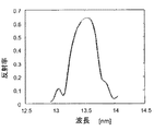
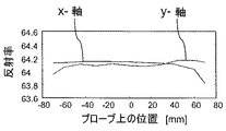
図3aから3cはドイツのベルリンにあるPhysikalisch Technische Bundesanstalt(PTB)でシンクロトロン放射を使用して行った直角入射反射の測定結果を示している。2通りの走査が行われた。1つはフォトマスク・ブランク70のx軸に沿って、1つはy軸に沿って行われ、6インチ平方のプレートであった。各走査は10箇所の測定点から構成される。
Example 1 Measurement Results Uniformity Figures 3a to 3c show the results of a normal incidence reflection measurement performed with synchrotron radiation at the Physikalisch Technische Bundesantalt (PTB) in Berlin, Germany. Two scans were performed. One was along the x-axis of the
図3bは測定した反射率のプロットで反射の均一性を6インチのプレートのx軸およびy軸に沿った位置の関数として示している。 FIG. 3b shows the reflectance uniformity as a function of position along the x and y axes of a 6 inch plate in a plot of measured reflectivity.
図3cは測定した中心波長のプロットでピーク反射の均一性を6インチのプレートのx軸88およびy軸84に沿った位置の関数として示している。
FIG. 3c shows the peak reflection uniformity as a function of position along the
図3bと3cそれぞれから理解できるように、フォトマスク・ブランク70の全面積にわたってピーク反射の均一性は±0.2%よりも優れており、中心波長の均一性は±0.02nmよりも優れている。
As can be seen from FIGS. 3b and 3c, respectively, the uniformity of the peak reflection over the entire area of the
図3aはx軸およびy軸に沿った2通りの走査の全20測定点の反射測定の結果を1つのプロットに一緒にして示している。反射率は波長nmの関数として示されており、均一性が優れていて20の曲線がプロット内で殆ど区別できないことが見てとれる。 FIG. 3a shows the results of the reflection measurement of all 20 measurement points of the two scans along the x and y axes together in one plot. The reflectivity is shown as a function of wavelength nm and it can be seen that the uniformity is excellent and the 20 curves are almost indistinguishable in the plot.
図4はフォトマスク・ブランク70の一部の断面の透過型電子顕微鏡画像を示している。基板50と多層積層71が示されている。全層が極めて平滑な表面を有し、偏りは識別不可能である。これは本発明の方法によって蒸着および処理された層もしくは膜の優れた均一性と再現性を示している。
FIG. 4 shows a transmission electron microscope image of a partial cross section of the
界面粗さ
図5はラスタ原子間力顕微鏡によって2層のMo/Si多層積層70、70’について為された表面測定を示している。左の縦列は10層の二重層のMo/Si多層積層70’に関する結果を示し、それに対して右の縦列は図2と4に示したような40層の二重層のMo/Si多層積層70に関する結果を示している。
Interface Roughness FIG. 5 shows surface measurements made on a two-layer Mo /
上側の横列は10μm×10μmの面積を表わす低倍率の結果を示し、それに対して下側の横列は1μm×1μmの面積を表わす高倍率の結果を示している。 The upper row shows low magnification results representing an area of 10 μm × 10 μm, while the lower row shows high magnification results representing an area of 1 μm × 1 μm.
2つのラスタ規模から、二重層の数を増加させることに関して表面粗さが上昇することはないことが見てとれる。したがって、本発明の方法で蒸着する間に表面粗さが上昇することはない。実際では、本発明によるイオンビーム蒸着は、少なくとも5層、10層もしくは40層でさえ、複数の層にわたって基板の粗さを再現する。少なくとも1層、最も好ましくは全層が<5nm rms、好ましくは<2nm rmsの表面粗さを有する。 From the two raster scales, it can be seen that the surface roughness does not increase with increasing number of bilayers. Therefore, the surface roughness does not increase during vapor deposition by the method of the present invention. In practice, ion beam deposition according to the invention reproduces the roughness of the substrate over a plurality of layers, at least 5, 10 or even 40 layers. At least one, most preferably all, layers have a surface roughness of <5 nm rms, preferably <2 nm rms.
図6は、蒸着処理の間に補助供給源60の第2のイオンビーム62によってフォトマスク・ブランクを処理すると表面の品質がさらに改善されることが可能であることを示している。実線の曲線は界面の処理もしくは設計を施していない50層の二重層の積層の反射率曲線である。破線は層界面の平坦化の形で界面の処理もしくは設計をして蒸着された30層の二重層しか有していない。表面品質の改善は、少ない数の層で同じ反射値、すなわち30層のみの二重層を使用して60%を超える反射率を達成することを可能にする。処理されたフォトマスク・ブランク70は同じ数の層を備えた未処理のフォトマスク・ブランクの反射率よりも少なくとも2%、5%、10%、20%高いピーク反射率を有することが好ましい。
FIG. 6 shows that treating the photomask blank with the
バイナリ・フォトマスク・ブランク
図7はバイナリ・フォトマスク・ブランク80の概略の断面を示している。バイナリ・フォトマスク・ブランク80は基板50上に蒸着された少なくとも2層87、88の吸収層の積層86を含む。
Binary Photomask Blank FIG. 7 shows a schematic cross section of a
第1の層87はたとえばクロム層であって必要な光学密度を達成し、それに対して第2の層88はたとえば酸化クロム層であって抗反射コーティングを提供する。この実施例では第1の層は48nmの厚さを有し、第2の層は22nmの厚さを有する。
The
実施例2の蒸着パラメータ
バイナリ・フォトマスク・ブランク80は上述のEUVフォトマスク・ブランク70の二重層72、73ほど薄い層を含まない。したがって、以下のような比較的高い蒸着パラメータが使用されることが可能である。
一次原子:アルゴン10sccm
一次エネルギー:1300eV
一次電流:350mA
背圧:2e−8Torr
蒸着圧:1e−4Torr
Example 2 Deposition Parameters
Primary atom: 10 sccm argon
Primary energy: 1300 eV
Primary current: 350 mA
Back pressure: 2e-8Torr
Deposition pressure: 1e-4Torr
両方の層に関するスパッタ・ターゲット40はクロム・ターゲットである。吸収層積層86の第2もしくは上の層88は、反射率を下げるために8sccmの酸素ガス流66を使用して酸素イオンを含む第2のイオンビーム62によってドープされる。
The
実施例2の測定結果
図8はバイナリ・フォトマスク・ブランク80に関して測定した光学密度を波長の関数として示している。層の積層もしくは系86は、この実施例では365nmである設計波長の領域で少なくとも光学密度3を達成するように設計される。
FIG. 8 shows the measured optical density for the binary photomask blank 80 as a function of wavelength. The layer stack or
図9は測定した反射率曲線を波長の関数として示している。層の積層もしくは系86は、365nmの設計波長で1/4波長条件を満たすように設計される。抗反射層88の厚さおよび酸素含有量は設計波長で≦12%の最小反射率を達成するように調整される。
FIG. 9 shows the measured reflectance curve as a function of wavelength. The layer stack or
図10は6インチのフォトマスク・ブランク80の表面にわたって365nmで二次元で測定した反射率の輪郭プロットを示している。都合のよいことに、フォトマスク・ブランク80にわたって±0.2%よりも優れた反射率の均一性が達成される。
FIG. 10 shows a contour plot of reflectivity measured in two dimensions at 365 nm over the surface of a 6
[実施例3、4、5]
位相シフト・フォトマスク・ブランク
図11aから11cは3つのタイプの位相シフト・フォトマスク・ブランク90、100、110の断面を示している。フォトマスク・ブランク90、100、110はそれぞれ180°の位相シフトを引き起こしてかつ約6%の透過率を有する位相シフト層構造91、101、111を含む。位相シフト層構造は一様もしくは複合の材料で作製された単層91、あるいは二重層101または多層111のいずれかである。後者の1つは増えた自由パラメータ数が理由となって改善された制御を可能にする。
[Examples 3, 4, and 5]
Phase Shift Photomask Blanks FIGS. 11a to 11c show cross sections of three types of phase shift photomask blanks 90,100,110. The
図11aは、透明基板50の表面の上に直接蒸着された複合の位相シフト構造91を備えた位相シフト・フォトマスク・ブランク90を示している。
FIG. 11 a shows a phase shift photomask blank 90 with a composite
図11bは、基板50の表面の上に接触して蒸着された二重層の位相シフト構造101を備えた位相シフト・フォトマスク・ブランク100を示している。二重層構造101は第1と第2の層102、103を含む。
FIG. 11 b shows a phase shift photomask blank 100 with a double layer
図11cは、基板50の上に成長した多層の位相シフト構造111を備えた位相シフト・フォトマスク・ブランク110を示している。多層構造111は10層の二重層102、103で構成される。
FIG. 11c shows a phase shift photomask blank 110 with a multilayer
位相シフト・フォトマスク・ブランク90、100、110の各々の位相シフト構造91、101、111は140nmの厚さを有する。さらに、70nmの厚さを備えた抗反射クロム層の対96と97、106と107、116と117がそれぞれの位相シフト層構造91、101、111の上に成長させられている。
The
図12は図11aに示した実施例による単層の位相シフトの計算を示している。図12から、180°の望ましい位相シフトが膜厚、それと同時に透過率を規定することが見てとれる。透過率は材料の光学定数を変えることによってのみ左右されることが可能である。したがって、構造設計に関してさらなる自由度は存在しない。 FIG. 12 shows the calculation of the phase shift of a single layer according to the embodiment shown in FIG. 11a. From FIG. 12, it can be seen that the desired phase shift of 180 ° defines the film thickness and, at the same time, the transmittance. The transmission can only be influenced by changing the optical constants of the material. Therefore, there is no further freedom with respect to the structural design.
図12では、異なる光学定数を備えた2つの材料に関する2つのプロット121と122が実線と破線によってそれぞれ示されている。それらのプロットから引き出すことができるように、それらの実施例に関して結果的に得られる膜厚は約80nmと約100nmであり、結果的に得られる透過率はそれぞれ約0.275と約0.1である。
In FIG. 12, two
図13は図11bに示した実施例による二重層の位相シフトの計算を示している。ここでは、第2の層103の膜厚は第1の層102の厚さに対する追加的な自由パラメータである。
FIG. 13 shows the calculation of the phase shift of the bilayer according to the embodiment shown in FIG. 11b. Here, the thickness of the
図13の左のプロットから、高い吸収性の層である第1の層102の厚さは所望の透過率に調整されることが可能であり、この実施例では約70nmの厚さで0.1が達成されることが見てとれる。
From the left plot of FIG. 13, the thickness of the
その後、180°の位相シフトを達成するために、低吸収性材料の成長層である第2の層103の厚さが調整される。図13の右のプロットから見てとれるように、第2の層の厚さは約30nmに選択される。
Thereafter, the thickness of the
2つの材料、すなわち第1の層102に関する目標透過率を調整するための高い吸収係数を備えた材料、および位相シフトを180°に調整するための第2の層103に関する低い吸収係数を備えた材料が使用される。この実施例では、吸収性の第1の層102についてはSiN、位相シフト用の第2の層103についてはSiO2が選択される。
Two materials, one with a high absorption coefficient to adjust the target transmittance for the
実施例3に関する蒸着パラメータ
層が比較的厚いので、以下のように高い蒸着パラメータが選択される。
一次原子:アルゴン10sccm
一次エネルギー:1300eV
一次電流:350mA
背圧:2e−8Torr
蒸着圧:1e−4Torr
Deposition Parameters for Example 3 Since the layers are relatively thick, the higher deposition parameters are selected as follows.
Primary atom: 10 sccm argon
Primary energy: 1300 eV
Primary current: 350 mA
Back pressure: 2e-8Torr
Deposition pressure: 1e-4Torr
スパッタ・ターゲット40としてシリコンおよびクロムのターゲットが使用される。
SiN層102は22sccmの流量を使用して窒素でドープされ、SiO2層103は15sccmの流量を使用して酸素でドープされる。窒素は補助の供給源60内でイオン化され、100Vの加速電圧を使用して基板50に向けて加速される。クロム層は図7に示したバイナリの実施例と同じである。
Silicon and chromium targets are used as sputter targets 40.
The
実施例3の測定結果
図14aと14bはSiNおよびSiO2の層102、103の光学定数の測定した分散を示している。測定のためにN&K分光光度計が使用された。
図14aはSiO2層103の屈折率131と減衰率132のプロットを示し、図14bはSiN層102の屈折率133と減衰率134のプロットを示し、各々が光の波長の関数である。
193nmに関する光学定数は次のように認められる。
Measurement Results of Example 3 FIGS. 14a and 14b show the measured dispersion of the optical constants of the SiN and SiO 2 layers 102, 103. An N & K spectrophotometer was used for the measurements.
FIG. 14a shows a plot of the
The optical constants for 193 nm are observed as follows.

これらの分散データを使用して、以下のパラメータで範例となる二重層の位相シフト・フォトマスク・ブランク100が設計される。
SiNの厚さ:27nm
SiO2の厚さ:92nm
相対透過率:6.2%
位相シフト:180°
Using these scattered data, an exemplary double layer phase
SiN thickness: 27 nm
SiO 2 thickness: 92 nm
Relative transmittance: 6.2%
Phase shift: 180 °
さらに、以下のパラメータで多層の位相シフト・フォトマスク・ブランク110が設計された。
各SiN層の厚さ:1.6nm
各SiO2層の厚さ:12.7nm
二重層の数:10
相対透過率:6.1%
位相シフト:180°
Further, a multilayer phase
Thickness of each SiN layer: 1.6 nm
Thickness of each SiO 2 layer: 12.7 nm
Number of double layers: 10
Relative transmittance: 6.1%
Phase shift: 180 °
両方の位相シフト・フォトマスク・ブランク100、110で、位相シフトは直接測定されなかったが、測定した分散データと測定した膜厚を使用して算出された。高精度で膜厚を判定するためにグレージング入射のX線反射計が使用された。
For both phase
[実施例6,7]
この実施例のバックグラウンドは、EUVフォトマスク・ブランク又はフォトマスクのEUV光学特性に対する、アルゴンとキセノンのそれぞれのスパッタリングガスの違いを示すことに有る。
[Examples 6 and 7]
The background of this example is to show the difference between the respective sputtering gases of argon and xenon on the EUV optical properties of the EUV photomask blank or photomask.
キセノンとアルゴンの異なる原子量に関連して、両実施例において、およそ等しい被覆条件となる安定なプロセスパラメータを見つけることが必要である。 With respect to the different atomic weights of xenon and argon, it is necessary in both examples to find stable process parameters with approximately equal coating conditions.
それゆえ、実施例6において、キセノンは4,5sccmのスパッタガスとして用いられ、イオンビーム中の一次キセノンイオンのエネルギーはおよそ900eVであり、イオンビーム電流は約200mAに設定された。純粋なイオンビームを得るために堆積源における、背圧は2e−8Torrとされ、キセノンの分圧は1e−4Torrに設定された。実施例6において被覆されたプローブは51のモリブデンとシリコンの二重層あるいは交互膜を含む。各層のペアが6.99nmの厚さを有する。この積層はEUVミラーに相当し、1つのシリコンの11nmキャップ層によって被覆された。 Therefore, in Example 6, xenon was used as a sputtering gas of 4.5 sccm, the energy of primary xenon ions in the ion beam was about 900 eV, and the ion beam current was set to about 200 mA. To obtain a pure ion beam, the back pressure at the deposition source was set to 2e-8 Torr, and the partial pressure of xenon was set to 1e-4 Torr. The probe coated in Example 6 contained 51 molybdenum and silicon bilayers or alternating membranes. Each layer pair has a thickness of 6.99 nm. This stack corresponded to an EUV mirror and was covered by one 11 nm cap layer of silicon.
実施例7において、アルゴンが10sccmのスパッタガスとして用いられ、イオンビーム中の一次アルゴンイオンのエネルギーはおよそ900eVであり、イオンビーム電流は約200mAに設定された。純粋なイオンビームを得るために堆積源における、背圧は2e−8Torrとされ、アルゴンの分圧は1e−4Torrに設定された。実施例7におけるプローブは、EUVミラーに相当する、48のモリブデンとシリコンの二重層あるいは交互膜を含む。各層のペアが6.92nmの厚さを有する。この層のペアは、1つのシリコンの11nmキャップ層によって被覆された。 In Example 7, argon was used as a sputtering gas of 10 sccm, the energy of primary argon ions in the ion beam was about 900 eV, and the ion beam current was set to about 200 mA. In order to obtain a pure ion beam, the back pressure at the deposition source was set to 2e-8 Torr, and the partial pressure of argon was set to 1e-4 Torr. The probe in Example 7 includes 48 molybdenum and silicon bilayers or alternating films, corresponding to EUV mirrors. Each layer pair has a thickness of 6.92 nm. This pair of layers was covered by one 11 nm cap layer of silicon.
図15はスパッタリングプロセス時にキセノンとアルゴンを用いた場合の反射率における違いを示した図である。実線は実施例7(アルゴンスパッタ)の反射率曲線を示し、破線は実施例6(キセノンスパッタ)の反射率曲線を示す。キセノンを用いた実施例6のプローブは、アルゴンを用いた実施例7のプローブの反射レートよりも高い反射レートを持っている。 FIG. 15 is a diagram showing a difference in reflectance when xenon and argon are used during the sputtering process. The solid line shows the reflectance curve of Example 7 (argon sputter), and the broken line shows the reflectance curve of Example 6 (xenon sputter). The probe of Example 6 using xenon has a higher reflection rate than the probe of Example 7 using argon.
発明者は、スパッタプロセス中にスパッタガスとしてキセノンを用いることによって、光学的、好ましくはフォトマスク・ブランクあるいはフォトマスクの光学的EUV特性を改善することを見出した。 The inventor has found that the use of xenon as a sputter gas during the sputtering process improves the optical, preferably the optical EUV properties of the photomask blank or photomask.
本発明、好ましい実施形態および特許請求項に引用された事項のすべての特徴が互いに組み合わされることが可能であり、説明した実施例の多くの詳細が本発明の範囲から逸脱することなく変更され得ることは当業者にとって明らかである。 All features of the invention, preferred embodiments and the subject matter recited in the claims can be combined with one another and many details of the described embodiments can be changed without departing from the scope of the invention This will be clear to those skilled in the art.
Claims (41)
真空チャンバ内に基板とターゲットを供給する工程、
第1の粒子ビームを供給する工程、
前記第1の粒子ビームで照射することによって前記ターゲットをスパッタリングする工程、
前記ターゲットの前記スパッタリングによって前記基板上に第1の材料の少なくとも第1の層を蒸着する工程を含む方法。 A method for manufacturing a photomask blank, in particular a binary photomask blank, a phase shift photomask blank or an extreme ultraviolet photomask blank, comprising:
Supplying a substrate and a target in a vacuum chamber,
Providing a first particle beam;
Sputtering the target by irradiating with the first particle beam;
Depositing at least a first layer of a first material on said substrate by said sputtering of said target.
−光学密度、
−エッチング時間、
−接着性および
−反射率
のうちの少なくとも1つが前記ドーピングによって制御される、請求項18に記載の方法。 The following parameters of at least one of the layers: optical density,
Etching time,
19. The method of claim 18, wherein at least one of -adhesion and -reflectance is controlled by the doping.
真空チャンバ内に基板とスパッタ・ターゲットを供給する工程、
蒸着粒子源および補助の粒子源を供給する工程、
前記蒸着および補助の粒子源によって第1および第2の粒子ビームをそれぞれ供給する工程、
前記第1の粒子ビームで照射することによって前記ターゲットをスパッタリングし、そこでは前記第1の粒子ビームが前記蒸着粒子源から前記ターゲット上へと向けられ、スパッタされた粒子が前記ターゲットから前記基板に対する方向へ現れる工程、
前記ターゲットの前記スパッタリングによって前記基板上に第1の材料の少なくとも第1の層を蒸着する(成長させる)工程、
前記ターゲットのスパッタリングによって前記第1の層の上に第2の材料の少なくとも第2の層を蒸着する(成長させる)工程、
前記基板または前記層のうちの少なくとも1層を処理するために前記第2の粒子ビームで前記フォトマスク・ブランクを照射する工程を含む方法。 A method for manufacturing a photomask blank, in particular a binary photomask blank, a phase shift photomask blank or an extreme ultraviolet photomask blank, comprising:
Supplying a substrate and a sputter target in a vacuum chamber,
Providing a vapor deposition particle source and an auxiliary particle source;
Supplying first and second particle beams by the deposition and auxiliary particle sources, respectively;
Sputtering the target by irradiating with the first particle beam, wherein the first particle beam is directed from the vapor deposition particle source onto the target, and the sputtered particles are directed from the target to the substrate. The process that appears in the direction,
Depositing (growing) at least a first layer of a first material on the substrate by sputtering of the target;
Depositing (growing) at least a second layer of a second material on the first layer by sputtering the target;
Irradiating the photomask blank with the second particle beam to treat the substrate or at least one of the layers.
真空チャンバ内に基板を供給する工程、
前記基板上に第1の材料の層を成長させる工程を含み、
前記層を成長させる前記工程がイオンビーム蒸着(IBD)によって実行される方法。 A method for manufacturing a photomask blank, in particular a binary photomask blank, a phase shift photomask blank or an extreme ultraviolet photomask blank, comprising:
Supplying a substrate into the vacuum chamber,
Growing a layer of a first material on the substrate,
The method wherein the step of growing the layer is performed by ion beam deposition (IBD).
基板および
イオンビーム蒸着によって前記基板の上に蒸着された1層または複数層を含むマスク・ブランク。 A mask blank, in particular a binary photomask blank, a phase shift photomask blank or an extreme ultraviolet photomask blank,
A mask blank comprising a substrate and one or more layers deposited on said substrate by ion beam deposition.
基板とターゲットが処理可能で排気に適した真空チャンバ、
前記ターゲットをスパッタリングし、前記基板上に少なくとも第1の層を蒸着するために前記ターゲットに向けられることが可能な第1の粒子ビームを供給するための蒸着粒子源、および
前記基板を処理するために前記基板に向けられることが可能な第2の粒子ビームを供給するための補助の粒子源を含む装置。 An apparatus for manufacturing a photomask blank, especially a binary photomask blank, a phase shift photomask blank or an extreme ultraviolet photomask blank,
A vacuum chamber that can process substrates and targets and is suitable for evacuation,
A vapor deposition particle source for sputtering the target and providing a first particle beam that can be directed at the target to deposit at least a first layer on the substrate; and for processing the substrate. Apparatus comprising an auxiliary particle source for providing a second particle beam that can be directed to said substrate.
−異なる方向性、
−異なる粒子、および
−異なる粒子エネルギー
のうちの少なくとも1つのビームを供給するのに適している、請求項37に記載の装置。
The deposition particle source and the auxiliary particle source,
-Different directions,
38. Apparatus according to claim 37, adapted to provide a beam of at least one of-different particles, and-different particle energies.
Applications Claiming Priority (1)
| Application Number | Priority Date | Filing Date | Title |
|---|---|---|---|
| US10/367,539 US20040159538A1 (en) | 2003-02-13 | 2003-02-13 | Photo mask blank, photo mask, method and apparatus for manufacturing of a photo mask blank |
Publications (1)
| Publication Number | Publication Date |
|---|---|
| JP2004246366A true JP2004246366A (en) | 2004-09-02 |
Family
ID=32850001
Family Applications (1)
| Application Number | Title | Priority Date | Filing Date |
|---|---|---|---|
| JP2004036249A Abandoned JP2004246366A (en) | 2003-02-13 | 2004-02-13 | Photomask blank, photomask, method and apparatus for manufacturing photomask blank |
Country Status (6)
| Country | Link |
|---|---|
| US (2) | US20040159538A1 (en) |
| JP (1) | JP2004246366A (en) |
| KR (1) | KR20040073400A (en) |
| CN (1) | CN1523444A (en) |
| DE (1) | DE102004006586A1 (en) |
| TW (1) | TW200420736A (en) |
Cited By (17)
| Publication number | Priority date | Publication date | Assignee | Title |
|---|---|---|---|---|
| WO2006030627A1 (en) * | 2004-09-17 | 2006-03-23 | Asahi Glass Company, Limited | Reflective mask blank for euv lithography and method for producing same |
| JP2007073949A (en) * | 2005-08-11 | 2007-03-22 | Hoya Corp | Method for manufacturing substrate with multilayer reflective film, method for manufacturing reflective mask blank, and method for manufacturing reflective mask |
| JP2007114336A (en) * | 2005-10-19 | 2007-05-10 | Hoya Corp | Reflective mask blank substrate manufacturing method, reflective mask blank manufacturing method, and reflective mask manufacturing method |
| JP2009519593A (en) * | 2005-12-13 | 2009-05-14 | コミシリア ア レネルジ アトミック | Reflective photolithography mask and method of making the mask |
| JP2009272317A (en) * | 2008-04-30 | 2009-11-19 | Hoya Corp | Method for manufacturing substrate with multilayer reflection film, method for manufacturing reflection type mask blank and method for manufacturing reflection type mask |
| JP2010135732A (en) * | 2008-08-01 | 2010-06-17 | Asahi Glass Co Ltd | Substrate for euv mask blanks |
| JP4858539B2 (en) * | 2005-10-03 | 2012-01-18 | 旭硝子株式会社 | Method for forming multilayer film of mask blank for EUV lithography, and method for manufacturing mask blank for EUV lithography |
| JP2013141039A (en) * | 2013-04-23 | 2013-07-18 | Hoya Corp | Method for manufacturing substrate with multilayer reflection film, method for manufacturing reflective mask blank, and method for manufacturing reflective mask |
| WO2014050831A1 (en) * | 2012-09-28 | 2014-04-03 | Hoya株式会社 | Method for manufacturing substrate with multilayer reflective film |
| JP2014130976A (en) * | 2012-12-29 | 2014-07-10 | Hoya Corp | Method of manufacturing substrate with multilayer reflection film, method of manufacturing reflective mask blank, and method of manufacturing reflective mask |
| JP2014130977A (en) * | 2012-12-29 | 2014-07-10 | Hoya Corp | Method of manufacturing substrate with multilayer reflection film, method of manufacturing reflective mask blank, and method of manufacturing reflective mask |
| KR20160061917A (en) * | 2013-09-27 | 2016-06-01 | 호야 가부시키가이샤 | Substrate provided with multilayer reflective film, mask blank, transfer mask, and semiconductor device production method |
| JP2017004008A (en) * | 2016-09-07 | 2017-01-05 | Hoya株式会社 | Mask blank, phase shift mask manufacturing method, and semiconductor device manufacturing method |
| JP2018109780A (en) * | 2018-03-02 | 2018-07-12 | Hoya株式会社 | Mask blank, phase shift mask and manufacturing method thereof |
| US10180622B2 (en) | 2013-01-15 | 2019-01-15 | Hoya Corporation | Mask blank, phase-shift mask, method of manufacturing mask blank, method of manufacturing phase-shift mask and method of manufacturing semiconductor device |
| JPWO2023136183A1 (en) * | 2022-01-13 | 2023-07-20 | ||
| KR20240007154A (en) | 2021-05-14 | 2024-01-16 | 에이지씨 가부시키가이샤 | Reflective mask blank and manufacturing method thereof, and substrate with reflective layer for the mask blank |
Families Citing this family (15)
| Publication number | Priority date | Publication date | Assignee | Title |
|---|---|---|---|---|
| WO2006040613A1 (en) * | 2004-10-13 | 2006-04-20 | Xenocs | Method of deposition with reduction of contaminants in an ion assist beam and associated apparatus |
| US7459095B2 (en) * | 2004-10-21 | 2008-12-02 | Corning Incorporated | Opaque chrome coating suitable for etching |
| KR100630728B1 (en) * | 2004-12-29 | 2006-10-02 | 삼성전자주식회사 | Reflective photomask and its manufacturing method |
| US7712333B2 (en) * | 2006-03-29 | 2010-05-11 | Asahi Glass Company, Limited | Method for smoothing a surface of a glass substrate for a reflective mask blank used in EUV lithography |
| DE102008042212A1 (en) * | 2008-09-19 | 2010-04-01 | Carl Zeiss Smt Ag | Reflective optical element and method for its production |
| KR101593388B1 (en) * | 2009-10-22 | 2016-02-12 | (주) 에스앤에스텍 | The Half-tone Phase Shift Blank Mask Half-tone Phase Shift Photomask and these Manufacturing Methods |
| US8562794B2 (en) * | 2010-12-14 | 2013-10-22 | Asahi Glass Company, Limited | Process for producing reflective mask blank for EUV lithography and process for producing substrate with functional film for the mask blank |
| JP6105490B2 (en) * | 2012-01-27 | 2017-03-29 | 旭化成株式会社 | Thermally reactive resist material for dry etching and mold manufacturing method |
| US8513619B1 (en) * | 2012-05-10 | 2013-08-20 | Kla-Tencor Corporation | Non-planar extractor structure for electron source |
| US20140272684A1 (en) * | 2013-03-12 | 2014-09-18 | Applied Materials, Inc. | Extreme ultraviolet lithography mask blank manufacturing system and method of operation therefor |
| JP6258151B2 (en) * | 2013-09-25 | 2018-01-10 | 信越化学工業株式会社 | Photomask blank and manufacturing method thereof |
| JP7027895B2 (en) * | 2017-02-09 | 2022-03-02 | 信越化学工業株式会社 | Photomask blank manufacturing method and photomask manufacturing method |
| JP7318565B2 (en) * | 2020-03-03 | 2023-08-01 | 信越化学工業株式会社 | Manufacturing method of reflective mask blank |
| US20230343557A1 (en) * | 2022-04-23 | 2023-10-26 | Plasma-Therm Nes Llc | Virtual shutter in ion beam system |
| CN119805851B (en) * | 2025-02-27 | 2025-12-12 | 中国科学院光电技术研究所 | Mask plate absorption layer preparation method, mask plate and preparation method thereof |
Family Cites Families (10)
| Publication number | Priority date | Publication date | Assignee | Title |
|---|---|---|---|---|
| US4793908A (en) * | 1986-12-29 | 1988-12-27 | Rockwell International Corporation | Multiple ion source method and apparatus for fabricating multilayer optical films |
| US4944754A (en) * | 1987-04-29 | 1990-07-31 | Vent-Plant Corporation | Method of manufacturing synthetic bone coated surgical implants |
| US4885070A (en) * | 1988-02-12 | 1989-12-05 | Leybold Aktiengesellschaft | Method and apparatus for the application of materials |
| US5055318A (en) * | 1988-10-11 | 1991-10-08 | Beamalloy Corporation | Dual ion beam ballistic alloying process |
| US6590324B1 (en) * | 1999-09-07 | 2003-07-08 | Veeco Instruments, Inc. | Charged particle beam extraction and formation apparatus |
| JP2002169265A (en) * | 2000-12-01 | 2002-06-14 | Hoya Corp | Photomask blank and method of manufacturing photomask blank |
| US6653027B2 (en) * | 2001-02-26 | 2003-11-25 | International Business Machines Corporation | Attenuated embedded phase shift photomask blanks |
| JP4071714B2 (en) * | 2001-10-24 | 2008-04-02 | カール・ツァイス・エスエムティー・アーゲー | Multilayer manufacturing method |
| US20030164998A1 (en) * | 2002-03-01 | 2003-09-04 | The Regents Of The University Of California | Ion-assisted deposition techniques for the planarization of topological defects |
| US6756161B2 (en) * | 2002-04-16 | 2004-06-29 | E. I. Du Pont De Nemours And Company | Ion-beam deposition process for manufacture of binary photomask blanks |
-
2003
- 2003-02-13 US US10/367,539 patent/US20040159538A1/en not_active Abandoned
- 2003-12-19 TW TW092136215A patent/TW200420736A/en unknown
-
2004
- 2004-02-10 DE DE102004006586A patent/DE102004006586A1/en not_active Withdrawn
- 2004-02-11 US US10/777,800 patent/US20040231971A1/en not_active Abandoned
- 2004-02-13 KR KR1020040009782A patent/KR20040073400A/en not_active Withdrawn
- 2004-02-13 CN CNA2004100049423A patent/CN1523444A/en active Pending
- 2004-02-13 JP JP2004036249A patent/JP2004246366A/en not_active Abandoned
Cited By (27)
| Publication number | Priority date | Publication date | Assignee | Title |
|---|---|---|---|---|
| WO2006030627A1 (en) * | 2004-09-17 | 2006-03-23 | Asahi Glass Company, Limited | Reflective mask blank for euv lithography and method for producing same |
| JP2007073949A (en) * | 2005-08-11 | 2007-03-22 | Hoya Corp | Method for manufacturing substrate with multilayer reflective film, method for manufacturing reflective mask blank, and method for manufacturing reflective mask |
| JP4858539B2 (en) * | 2005-10-03 | 2012-01-18 | 旭硝子株式会社 | Method for forming multilayer film of mask blank for EUV lithography, and method for manufacturing mask blank for EUV lithography |
| JP2007114336A (en) * | 2005-10-19 | 2007-05-10 | Hoya Corp | Reflective mask blank substrate manufacturing method, reflective mask blank manufacturing method, and reflective mask manufacturing method |
| JP2009519593A (en) * | 2005-12-13 | 2009-05-14 | コミシリア ア レネルジ アトミック | Reflective photolithography mask and method of making the mask |
| JP2009272317A (en) * | 2008-04-30 | 2009-11-19 | Hoya Corp | Method for manufacturing substrate with multilayer reflection film, method for manufacturing reflection type mask blank and method for manufacturing reflection type mask |
| JP2014033221A (en) * | 2008-08-01 | 2014-02-20 | Asahi Glass Co Ltd | Substrate for euv mask blanks |
| JP2010135732A (en) * | 2008-08-01 | 2010-06-17 | Asahi Glass Co Ltd | Substrate for euv mask blanks |
| KR20150058149A (en) * | 2012-09-28 | 2015-05-28 | 호야 가부시키가이샤 | Method for manufacturing substrate with multilayer reflective film |
| WO2014050831A1 (en) * | 2012-09-28 | 2014-04-03 | Hoya株式会社 | Method for manufacturing substrate with multilayer reflective film |
| JPWO2014050831A1 (en) * | 2012-09-28 | 2016-08-22 | Hoya株式会社 | Manufacturing method of substrate with multilayer reflective film |
| US9507254B2 (en) | 2012-09-28 | 2016-11-29 | Hoya Corporation | Method of manufacturing substrate with a multilayer reflective film, method of manufacturing a reflective mask blank, substrate with a multilayer reflective film, reflective mask blank, reflective mask and method of manufacturing a semiconductor device |
| KR102180712B1 (en) * | 2012-09-28 | 2020-11-19 | 호야 가부시키가이샤 | Method for manufacturing substrate with multilayer reflective film |
| JP2014130976A (en) * | 2012-12-29 | 2014-07-10 | Hoya Corp | Method of manufacturing substrate with multilayer reflection film, method of manufacturing reflective mask blank, and method of manufacturing reflective mask |
| JP2014130977A (en) * | 2012-12-29 | 2014-07-10 | Hoya Corp | Method of manufacturing substrate with multilayer reflection film, method of manufacturing reflective mask blank, and method of manufacturing reflective mask |
| US10539866B2 (en) | 2013-01-15 | 2020-01-21 | Hoya Corporation | Mask blank, phase-shift mask, and method of manufacturing semiconductor device |
| US10942442B2 (en) | 2013-01-15 | 2021-03-09 | Hoya Corporation | Mask blank, phase-shift mask, and method of manufacturing semiconductor device |
| US10180622B2 (en) | 2013-01-15 | 2019-01-15 | Hoya Corporation | Mask blank, phase-shift mask, method of manufacturing mask blank, method of manufacturing phase-shift mask and method of manufacturing semiconductor device |
| JP2013141039A (en) * | 2013-04-23 | 2013-07-18 | Hoya Corp | Method for manufacturing substrate with multilayer reflection film, method for manufacturing reflective mask blank, and method for manufacturing reflective mask |
| KR20160061917A (en) * | 2013-09-27 | 2016-06-01 | 호야 가부시키가이샤 | Substrate provided with multilayer reflective film, mask blank, transfer mask, and semiconductor device production method |
| KR102253519B1 (en) | 2013-09-27 | 2021-05-18 | 호야 가부시키가이샤 | Substrate provided with multilayer reflective film, mask blank, transfer mask, and semiconductor device production method |
| JP2017004008A (en) * | 2016-09-07 | 2017-01-05 | Hoya株式会社 | Mask blank, phase shift mask manufacturing method, and semiconductor device manufacturing method |
| JP2018109780A (en) * | 2018-03-02 | 2018-07-12 | Hoya株式会社 | Mask blank, phase shift mask and manufacturing method thereof |
| KR20240007154A (en) | 2021-05-14 | 2024-01-16 | 에이지씨 가부시키가이샤 | Reflective mask blank and manufacturing method thereof, and substrate with reflective layer for the mask blank |
| JPWO2023136183A1 (en) * | 2022-01-13 | 2023-07-20 | ||
| WO2023136183A1 (en) * | 2022-01-13 | 2023-07-20 | Agc株式会社 | Reflection-type mask blank, reflection-type mask, and method for producing reflection-type mask |
| JP7480927B2 (en) | 2022-01-13 | 2024-05-10 | Agc株式会社 | Reflective mask blank, reflective mask, and method for manufacturing reflective mask |
Also Published As
| Publication number | Publication date |
|---|---|
| CN1523444A (en) | 2004-08-25 |
| KR20040073400A (en) | 2004-08-19 |
| DE102004006586A1 (en) | 2004-11-11 |
| TW200420736A (en) | 2004-10-16 |
| US20040159538A1 (en) | 2004-08-19 |
| US20040231971A1 (en) | 2004-11-25 |
Similar Documents
| Publication | Publication Date | Title |
|---|---|---|
| JP2004246366A (en) | Photomask blank, photomask, method and apparatus for manufacturing photomask blank | |
| US20210278759A1 (en) | Method of manufacturing reflective mask blank, and reflective mask blank | |
| US6295164B1 (en) | Multi-layered mirror | |
| US20220035234A1 (en) | Reflective mask blank for euv lithography, mask blank for euv lithography, and manufacturing methods thereof | |
| US8076055B2 (en) | Passivation of multi-layer mirror for extreme ultraviolet lithography | |
| US7282305B2 (en) | Reflective mask blank having a programmed defect and method of producing the same, reflective mask having a programmed defect and method of producing the same, and substrate for use in producing the reflective mask blank or the reflective mask having a programmed defect | |
| KR102207245B1 (en) | Amorphous layer extreme ultraviolet lithography blank, and manufacturing and lithography systems therefor | |
| US7326502B2 (en) | Multilayer coatings for EUV mask substrates | |
| JP7368564B2 (en) | Substrate with multilayer reflective film, reflective mask blank, reflective mask, and semiconductor device manufacturing method | |
| US7517617B2 (en) | Mask blank for use in EUV lithography and method for its production | |
| CN103930805B (en) | Method for producing a capping layer composed of silicon oxide on an EUV mirror, EUV mirror and EUV lithography apparatus | |
| EP1421443A2 (en) | Damascene extreme ultraviolet lithography alternative phase shift photomask and method of making | |
| KR20140138595A (en) | Method for manufacturing substrate provided with multilayer reflection film, method for manufacturing reflective mask blank, and method for manufacturing reflective mask | |
| JP7379027B2 (en) | Substrate with multilayer reflective film, reflective mask blank, reflective mask, and semiconductor device manufacturing method | |
| WO2007043488A1 (en) | Method for depositing multilayer film of mask blank for euv lithography and method for producing mask blank for euv lithography | |
| US8081384B2 (en) | Multilayer reflective film coated substrate, manufacturing method thereof, reflective mask blank, and reflective mask | |
| TW202034062A (en) | Extreme ultraviolet mask absorber materials | |
| US6905801B2 (en) | High performance EUV mask | |
| TW202141167A (en) | Extreme ultraviolet mask absorber materials | |
| JP2005529362A (en) | Photomask and defect repair method | |
| JP2023511124A (en) | Extreme UV mask blank hard mask material | |
| TWI754500B (en) | Mask blanks and methods for forming the same | |
| TW593708B (en) | Ion-beam deposition process for manufacturing attenuated phase shift photomask blanks | |
| CN113138528A (en) | Extreme ultraviolet mask and method for manufacturing the same | |
| US7804648B2 (en) | Multilayer reflective film coated substrate, manufacturing method thereof, reflective mask blank, and reflective mask |
Legal Events
| Date | Code | Title | Description |
|---|---|---|---|
| A711 | Notification of change in applicant |
Free format text: JAPANESE INTERMEDIATE CODE: A711 Effective date: 20050831 |
|
| RD03 | Notification of appointment of power of attorney |
Free format text: JAPANESE INTERMEDIATE CODE: A7423 Effective date: 20051018 |
|
| RD04 | Notification of resignation of power of attorney |
Free format text: JAPANESE INTERMEDIATE CODE: A7424 Effective date: 20051205 |
|
| A621 | Written request for application examination |
Free format text: JAPANESE INTERMEDIATE CODE: A621 Effective date: 20070202 |
|
| A762 | Written abandonment of application |
Free format text: JAPANESE INTERMEDIATE CODE: A762 Effective date: 20070726 |