JP2004252425A - Laser module and manufacturing method therefor - Google Patents
Laser module and manufacturing method therefor Download PDFInfo
- Publication number
- JP2004252425A JP2004252425A JP2003433527A JP2003433527A JP2004252425A JP 2004252425 A JP2004252425 A JP 2004252425A JP 2003433527 A JP2003433527 A JP 2003433527A JP 2003433527 A JP2003433527 A JP 2003433527A JP 2004252425 A JP2004252425 A JP 2004252425A
- Authority
- JP
- Japan
- Prior art keywords
- package
- semiconductor laser
- optical fiber
- laser
- laser module
- Prior art date
- Legal status (The legal status is an assumption and is not a legal conclusion. Google has not performed a legal analysis and makes no representation as to the accuracy of the status listed.)
- Pending
Links
- 238000004519 manufacturing process Methods 0.000 title claims description 15
- 239000004065 semiconductor Substances 0.000 claims abstract description 82
- 239000013307 optical fiber Substances 0.000 claims abstract description 71
- 230000003287 optical effect Effects 0.000 claims abstract description 21
- 230000008878 coupling Effects 0.000 claims abstract description 3
- 238000010168 coupling process Methods 0.000 claims abstract description 3
- 238000005859 coupling reaction Methods 0.000 claims abstract description 3
- 239000007789 gas Substances 0.000 claims description 33
- 229910000679 solder Inorganic materials 0.000 claims description 20
- 239000000853 adhesive Substances 0.000 claims description 13
- 230000001070 adhesive effect Effects 0.000 claims description 13
- 238000000034 method Methods 0.000 claims description 13
- 238000007872 degassing Methods 0.000 claims description 11
- 239000011261 inert gas Substances 0.000 claims description 11
- 238000003466 welding Methods 0.000 claims description 11
- QVGXLLKOCUKJST-UHFFFAOYSA-N atomic oxygen Chemical compound [O] QVGXLLKOCUKJST-UHFFFAOYSA-N 0.000 claims description 10
- 239000003550 marker Substances 0.000 claims description 10
- 229910052760 oxygen Inorganic materials 0.000 claims description 10
- 239000001301 oxygen Substances 0.000 claims description 10
- 230000004927 fusion Effects 0.000 claims description 9
- 150000002366 halogen compounds Chemical class 0.000 claims description 7
- 125000005843 halogen group Chemical group 0.000 claims description 7
- 230000010355 oscillation Effects 0.000 claims description 3
- 239000005416 organic matter Substances 0.000 claims 1
- 230000005540 biological transmission Effects 0.000 abstract description 6
- 230000000694 effects Effects 0.000 description 18
- 239000011248 coating agent Substances 0.000 description 14
- 238000000576 coating method Methods 0.000 description 14
- IJGRMHOSHXDMSA-UHFFFAOYSA-N Atomic nitrogen Chemical compound N#N IJGRMHOSHXDMSA-UHFFFAOYSA-N 0.000 description 12
- 229910004298 SiO 2 Inorganic materials 0.000 description 12
- 239000000428 dust Substances 0.000 description 12
- 239000012298 atmosphere Substances 0.000 description 11
- 238000007789 sealing Methods 0.000 description 10
- 239000000835 fiber Substances 0.000 description 9
- 239000000356 contaminant Substances 0.000 description 8
- 239000000460 chlorine Substances 0.000 description 7
- 239000000126 substance Substances 0.000 description 7
- 230000006866 deterioration Effects 0.000 description 6
- 229910052757 nitrogen Inorganic materials 0.000 description 6
- 239000000758 substrate Substances 0.000 description 6
- 238000011109 contamination Methods 0.000 description 5
- 239000011368 organic material Substances 0.000 description 5
- 239000011347 resin Substances 0.000 description 5
- 229920005989 resin Polymers 0.000 description 5
- 239000010980 sapphire Substances 0.000 description 5
- 229910052594 sapphire Inorganic materials 0.000 description 5
- 229910052801 chlorine Inorganic materials 0.000 description 4
- 150000001875 compounds Chemical class 0.000 description 4
- 229910052736 halogen Inorganic materials 0.000 description 4
- 150000002367 halogens Chemical class 0.000 description 4
- 150000002430 hydrocarbons Chemical class 0.000 description 4
- 230000008569 process Effects 0.000 description 4
- JMASRVWKEDWRBT-UHFFFAOYSA-N Gallium nitride Chemical compound [Ga]#N JMASRVWKEDWRBT-UHFFFAOYSA-N 0.000 description 3
- 229910052731 fluorine Inorganic materials 0.000 description 3
- QGZKDVFQNNGYKY-UHFFFAOYSA-N Ammonia Chemical compound N QGZKDVFQNNGYKY-UHFFFAOYSA-N 0.000 description 2
- 239000004215 Carbon black (E152) Substances 0.000 description 2
- ZAMOUSCENKQFHK-UHFFFAOYSA-N Chlorine atom Chemical compound [Cl] ZAMOUSCENKQFHK-UHFFFAOYSA-N 0.000 description 2
- YCKRFDGAMUMZLT-UHFFFAOYSA-N Fluorine atom Chemical compound [F] YCKRFDGAMUMZLT-UHFFFAOYSA-N 0.000 description 2
- VYPSYNLAJGMNEJ-UHFFFAOYSA-N Silicium dioxide Chemical compound O=[Si]=O VYPSYNLAJGMNEJ-UHFFFAOYSA-N 0.000 description 2
- MCMNRKCIXSYSNV-UHFFFAOYSA-N Zirconium dioxide Chemical compound O=[Zr]=O MCMNRKCIXSYSNV-UHFFFAOYSA-N 0.000 description 2
- 238000005253 cladding Methods 0.000 description 2
- 238000004891 communication Methods 0.000 description 2
- 239000002019 doping agent Substances 0.000 description 2
- 239000011737 fluorine Substances 0.000 description 2
- 125000001153 fluoro group Chemical group F* 0.000 description 2
- 239000011521 glass Substances 0.000 description 2
- 229930195733 hydrocarbon Natural products 0.000 description 2
- 230000007774 longterm Effects 0.000 description 2
- 239000000203 mixture Substances 0.000 description 2
- 239000012299 nitrogen atmosphere Substances 0.000 description 2
- 238000006552 photochemical reaction Methods 0.000 description 2
- 238000006303 photolysis reaction Methods 0.000 description 2
- XCZXGTMEAKBVPV-UHFFFAOYSA-N trimethylgallium Chemical compound C[Ga](C)C XCZXGTMEAKBVPV-UHFFFAOYSA-N 0.000 description 2
- ZCYVEMRRCGMTRW-UHFFFAOYSA-N 7553-56-2 Chemical group [I] ZCYVEMRRCGMTRW-UHFFFAOYSA-N 0.000 description 1
- 229910017980 Ag—Sn Inorganic materials 0.000 description 1
- 229910015363 Au—Sn Inorganic materials 0.000 description 1
- WKBOTKDWSSQWDR-UHFFFAOYSA-N Bromine atom Chemical group [Br] WKBOTKDWSSQWDR-UHFFFAOYSA-N 0.000 description 1
- MHYQBXJRURFKIN-UHFFFAOYSA-N C1(C=CC=C1)[Mg] Chemical compound C1(C=CC=C1)[Mg] MHYQBXJRURFKIN-UHFFFAOYSA-N 0.000 description 1
- OKTJSMMVPCPJKN-UHFFFAOYSA-N Carbon Chemical compound [C] OKTJSMMVPCPJKN-UHFFFAOYSA-N 0.000 description 1
- KZBUYRJDOAKODT-UHFFFAOYSA-N Chlorine Chemical compound ClCl KZBUYRJDOAKODT-UHFFFAOYSA-N 0.000 description 1
- RYGMFSIKBFXOCR-UHFFFAOYSA-N Copper Chemical compound [Cu] RYGMFSIKBFXOCR-UHFFFAOYSA-N 0.000 description 1
- 229910000881 Cu alloy Inorganic materials 0.000 description 1
- MYMOFIZGZYHOMD-UHFFFAOYSA-N Dioxygen Chemical compound O=O MYMOFIZGZYHOMD-UHFFFAOYSA-N 0.000 description 1
- 239000004593 Epoxy Substances 0.000 description 1
- 229910020174 Pb-In Inorganic materials 0.000 description 1
- BLRPTPMANUNPDV-UHFFFAOYSA-N Silane Chemical compound [SiH4] BLRPTPMANUNPDV-UHFFFAOYSA-N 0.000 description 1
- 239000006087 Silane Coupling Agent Substances 0.000 description 1
- 229910020816 Sn Pb Inorganic materials 0.000 description 1
- 229910020922 Sn-Pb Inorganic materials 0.000 description 1
- 229910018956 Sn—In Inorganic materials 0.000 description 1
- 229910008783 Sn—Pb Inorganic materials 0.000 description 1
- NINIDFKCEFEMDL-UHFFFAOYSA-N Sulfur Chemical compound [S] NINIDFKCEFEMDL-UHFFFAOYSA-N 0.000 description 1
- 230000004913 activation Effects 0.000 description 1
- 125000002723 alicyclic group Chemical group 0.000 description 1
- 229910021529 ammonia Inorganic materials 0.000 description 1
- 230000015572 biosynthetic process Effects 0.000 description 1
- 229910052799 carbon Inorganic materials 0.000 description 1
- 230000003197 catalytic effect Effects 0.000 description 1
- 239000000919 ceramic Substances 0.000 description 1
- 125000001309 chloro group Chemical group Cl* 0.000 description 1
- 239000002131 composite material Substances 0.000 description 1
- 229910052802 copper Inorganic materials 0.000 description 1
- 239000010949 copper Substances 0.000 description 1
- 230000000593 degrading effect Effects 0.000 description 1
- 229910001882 dioxygen Inorganic materials 0.000 description 1
- KPUWHANPEXNPJT-UHFFFAOYSA-N disiloxane Chemical class [SiH3]O[SiH3] KPUWHANPEXNPJT-UHFFFAOYSA-N 0.000 description 1
- 238000001312 dry etching Methods 0.000 description 1
- 239000003344 environmental pollutant Substances 0.000 description 1
- 238000005530 etching Methods 0.000 description 1
- 238000007667 floating Methods 0.000 description 1
- 230000004907 flux Effects 0.000 description 1
- -1 for example Chemical compound 0.000 description 1
- 238000010438 heat treatment Methods 0.000 description 1
- 230000006872 improvement Effects 0.000 description 1
- 239000012535 impurity Substances 0.000 description 1
- 239000003999 initiator Substances 0.000 description 1
- 238000009434 installation Methods 0.000 description 1
- 229910052740 iodine Inorganic materials 0.000 description 1
- 238000001459 lithography Methods 0.000 description 1
- 239000000463 material Substances 0.000 description 1
- 229910052751 metal Inorganic materials 0.000 description 1
- 239000002184 metal Substances 0.000 description 1
- 239000005304 optical glass Substances 0.000 description 1
- 150000003961 organosilicon compounds Chemical group 0.000 description 1
- 125000003566 oxetanyl group Chemical group 0.000 description 1
- 230000002093 peripheral effect Effects 0.000 description 1
- 238000005498 polishing Methods 0.000 description 1
- 231100000719 pollutant Toxicity 0.000 description 1
- 229920000642 polymer Polymers 0.000 description 1
- 238000002360 preparation method Methods 0.000 description 1
- 238000003825 pressing Methods 0.000 description 1
- 230000005855 radiation Effects 0.000 description 1
- 239000002994 raw material Substances 0.000 description 1
- 230000009467 reduction Effects 0.000 description 1
- 150000003839 salts Chemical class 0.000 description 1
- 229910000077 silane Inorganic materials 0.000 description 1
- 229910052814 silicon oxide Inorganic materials 0.000 description 1
- 239000007787 solid Substances 0.000 description 1
- 229910052717 sulfur Inorganic materials 0.000 description 1
- 239000011593 sulfur Substances 0.000 description 1
- 229910052724 xenon Inorganic materials 0.000 description 1
- FHNFHKCVQCLJFQ-UHFFFAOYSA-N xenon atom Chemical compound [Xe] FHNFHKCVQCLJFQ-UHFFFAOYSA-N 0.000 description 1
Images



Landscapes
- Optical Couplings Of Light Guides (AREA)
- Semiconductor Lasers (AREA)
Abstract
Description
本発明はレーザモジュールおよびその製造方法に関し、特に、半導体レーザ素子と、光ファイバと、半導体レーザ素子から出射したレーザビームを光ファイバの一端面に結合させる集光光学系とを備えたレーザモジュールおよびその製造方法に関するものである。 The present invention relates to a laser module and a manufacturing method thereof, and in particular, a laser module including a semiconductor laser element, an optical fiber, and a condensing optical system for coupling a laser beam emitted from the semiconductor laser element to one end face of the optical fiber, and It relates to the manufacturing method.
従来より、パッケージ内に収容された半導体レーザ素子と、一端(光入射端)がこのパッケージの内部を臨む状態にして該パッケージに固定された光ファイバと、半導体レーザ素子から出射されたレーザビームを光ファイバの光入射端に結合させる集光光学系とを備えてなるレーザモジュールは、いわゆるピッグテール型レーザモジュールとして、光通信部品として一般的に知られている。 Conventionally, a semiconductor laser element housed in a package, an optical fiber fixed to the package with one end (light incident end) facing the inside of the package, and a laser beam emitted from the semiconductor laser element A laser module including a condensing optical system coupled to a light incident end of an optical fiber is generally known as an optical communication component as a so-called pigtail laser module.
レーザモジュール内部においては、半導体レーザと光ファイバの光入射端とが光学的に結合された状態をマイクロメートルオーダで安定的に維持するために、光ファイバおよび集光光学系等は、通常、半田、溶接もしくは接着剤等の接着手段を用いて固定されている。 Inside the laser module, in order to stably maintain the optically coupled state of the semiconductor laser and the light incident end of the optical fiber on the order of micrometers, the optical fiber and the focusing optical system are usually soldered. It is fixed using an adhesive means such as welding or an adhesive.
また、通信用レーザモジュールでは、外気の湿気などによるレーザ劣化を防ぐために、パッケージを気密封止することが一般的に行われている、いわゆるCANパッケージに代表される構造は、半導体レーザ素子、およびレーザ端面を保護する封止構造として代表的である。このレーザモジュールにおいて、気密封止されたパッケージ内に残存する汚染物質が半導体レーザ素子の出射端面、集光光学系および光ファイバ等の光学部品に付着して、レーザ特性を劣化させるという問題がある。特に、光密度の高い部分において物質が付着する効果(集塵効果)が顕著である。さらに、GaN系半導体レーザ素子等の350〜500nm(400nm帯)の波長のレーザビームを出射する半導体レーザ素子を備えたレーザモジュールにおいては、光子エネルギーが高く、物質との光化学反応がより起きやすくなるために、集塵効果がより顕著に現れる。 In addition, in a communication laser module, in order to prevent laser deterioration due to moisture in the outside air, the structure typically represented by a so-called CAN package, in which the package is hermetically sealed, includes a semiconductor laser element, and It is representative as a sealing structure for protecting the laser end face. In this laser module, there is a problem that contaminants remaining in the hermetically sealed package adhere to optical components such as the emission end face of the semiconductor laser element, the condensing optical system, and the optical fiber, thereby degrading the laser characteristics. . In particular, the effect of adhering substances (dust collection effect) in a portion having a high light density is remarkable. Furthermore, in a laser module including a semiconductor laser element that emits a laser beam having a wavelength of 350 to 500 nm (400 nm band), such as a GaN-based semiconductor laser element, the photon energy is high and a photochemical reaction with a substance is more likely to occur. Therefore, the dust collection effect appears more prominently.
汚染物質の1つとしては、製造工程の雰囲気中から混入する炭化水素化合物等が挙げられ、この炭化水素が、レーザ光により重合あるいは分解されて分解物が付着し、出力の向上を妨げることが知られている。 As one of the pollutants, hydrocarbon compounds mixed in from the atmosphere of the manufacturing process can be cited, and this hydrocarbon is polymerized or decomposed by laser light, and decomposed substances adhere to it, preventing improvement in output. Are known.
また、空中を浮遊している低分子シロキサンが紫外線による光化学反応で酸素と反応し、光学ガラス窓部品にSiOxの形で堆積、付着することが開示されており、このため、大気と接する「窓」部材の定期的な交換を推奨している(例えば、特許文献1参照)。 In addition, it is disclosed that low molecular weight siloxane floating in the air reacts with oxygen by photochemical reaction by ultraviolet rays, and deposits and adheres to optical glass window parts in the form of SiOx. It is recommended to replace the member regularly (see, for example, Patent Document 1).
そこで、この集塵効果を防止するために、種々の提案がなされている。例えば、炭化水素化合物等を分解することを目的とした酸素を100ppm以上封止ガスに混入させることが提案されている(例えば、特許文献2参照)。 Therefore, various proposals have been made to prevent the dust collection effect. For example, it has been proposed to mix 100 ppm or more of oxygen for the purpose of decomposing hydrocarbon compounds into a sealing gas (see, for example, Patent Document 2).
また、400nm以下の紫外線を光学部品に照射する光学系において、光学部品の雰囲気を99.9%以上の窒素とすることが提案されている(例えば、特許文献3参照)。 In an optical system that irradiates an optical component with ultraviolet rays of 400 nm or less, it has been proposed that the atmosphere of the optical component is 99.9% or more of nitrogen (see, for example, Patent Document 3).
さらに、パッケージを封止する直前に、パッケージ内部の脱気処理を行うことが集塵効果の防止に効果があることも知られている。
しかしながら、一般に市販されているUV硬化樹脂による1次被膜およびポリマーによる2次被膜が施された光ファイバを備えた、パッケージに光ファイバが固定されたレーザモジュールの場合、パッケージに光ファイバが固定された状態で脱気処理を行うため、脱気処理装置中にファイバ被膜が存在することとなり、脱気処理中にこの被膜から脱ガス成分が発生し、このガスによりかえってモジュール内部が汚染されることになる。 However, in the case of a laser module in which an optical fiber is fixed to a package, which is provided with an optical fiber having a primary coating made of UV curable resin and a secondary coating made of a polymer that are generally commercially available, the optical fiber is fixed to the package. Since the degassing process is performed in the wet state, a fiber coating is present in the degassing device, and a degassing component is generated from the coating during the degassing process. become.
この汚染を防ぐために、予め光ファイバの被覆を全て除去することが考えられるが、被覆のない光ファイバは簡単に折れてしまうため扱い辛く実用性が低い。 In order to prevent this contamination, it is conceivable to remove all the coating of the optical fiber in advance. However, since the optical fiber without the coating is easily broken, it is difficult to handle and is not practical.
本発明は上記事情に鑑み汚染物質の付着を抑制した高信頼性が得られるレーザモジュールおよびその製造方法を提供することを目的とするものである。 In view of the above circumstances, an object of the present invention is to provide a laser module and a method for manufacturing the same that can achieve high reliability while suppressing adhesion of contaminants.
本発明のレーザモジュールは、光出射窓に光透過部材を備えた、気密封止されたパッケージと、
前記パッケージの内部に配置された1つもしくは複数の半導体レーザ素子と、
前記パッケージの外部に配置された光ファイバと、
前記半導体レーザ素子から出射されたレーザビームを前記光透過部材の外面上に集光させる、前記パッケージの内部に配置された集光光学系とを備え、
前記光ファイバの入射端が、前記光透過部材の外面の、前記レーザビームが集光する位置に密着して固定されていることを特徴とするものである。
The laser module of the present invention includes a hermetically sealed package including a light transmitting member in a light exit window,
One or more semiconductor laser elements disposed inside the package;
An optical fiber disposed outside the package;
A condensing optical system disposed inside the package for condensing a laser beam emitted from the semiconductor laser element on an outer surface of the light transmitting member;
The incident end of the optical fiber is fixed in close contact with a position on the outer surface of the light transmitting member where the laser beam is condensed.
なお、前記光透過部材に、前記レーザビームを集光させる位置を定めるためのマーカが付されていることが望ましい。光透過部材としては、前記レーザビームが透過可能な部材であればよく、円形平板、平行平板、レンズ、楔形等のいかなる形状でもよい。 In addition, it is desirable that a marker for determining a position for condensing the laser beam is attached to the light transmitting member. The light transmitting member may be any member that can transmit the laser beam, and may have any shape such as a circular flat plate, a parallel flat plate, a lens, and a wedge shape.
なお、ここで「密着して固定」とは、密着させて接着して固定した状態と、取外し可能に密着させて保持して固定した状態を含むものである。 Here, the term “closely fixed” includes a state in which it is closely attached and adhered and fixed, and a state in which it is detachably adhered and held and fixed.
前記半導体レーザ素子の発振波長が350nm〜500nmのレーザモジュールに本発明は好適である。具体的には、GaN系の半導体から構成されるものが挙げられる。 The present invention is suitable for a laser module in which the oscillation wavelength of the semiconductor laser element is 350 nm to 500 nm. Specifically, those composed of GaN-based semiconductors can be mentioned.
前記光ファイバの入射端がフェルールに挿入されており、前記パッケージを、前記フェルールと嵌合する装着器を備えたものとしてもよい。 The incident end of the optical fiber may be inserted into a ferrule, and the package may include a mounting device that fits the ferrule.
パッケージは、内部が不活性ガスで満たされているものであることが望ましく、該不活性ガスには、1ppm以上の濃度の酸素、ハロゲン族ガス、および/またはハロゲン化合物ガスが混入されていることがより望ましい。すなわち第1のパッケージの内部雰囲気としては、(1)不活性ガスと1ppm以上の濃度の酸素との混合ガス、(2)不活性ガスと、ハロゲン族ガスおよびハロゲン化合物ガスのうち少なくともいずれか一方のガスとの混合ガス(3)不活性ガスと、1ppm以上の濃度酸素と、ハロゲン族ガスおよびハロゲン化合物ガスのうち少なくともいずれか一方のガスとの混合ガスのいずれかであることがより望ましい。 The package is preferably filled with an inert gas, and the inert gas contains oxygen, a halogen group gas, and / or a halogen compound gas at a concentration of 1 ppm or more. Is more desirable. That is, the internal atmosphere of the first package includes (1) a mixed gas of an inert gas and oxygen having a concentration of 1 ppm or more, and (2) at least one of an inert gas, a halogen group gas, and a halogen compound gas. (3) A mixed gas of an inert gas, oxygen gas with a concentration of 1 ppm or more, and at least one of a halogen group gas and a halogen compound gas is more preferable.
また、パッケージは、フラックスフリー半田もしくはSi系有機物を含まない接着剤を使用して、あるいは融着もしくは溶接により気密封止されていることが望ましい。 The package is preferably hermetically sealed using flux-free solder or an adhesive that does not contain Si-based organic materials, or by fusion or welding.
半導体レーザ素子としては、アレイ状に並べられた複数のシングルキャビティ半導体レーザ素子、1つのマルチキャビティ半導体レーザ素子、アレイ状に並べられた複数のマルチキャビティ半導体レーザ素子、およびシングルキャビティ半導体レーザ素子とマルチキャビティ半導体レーザ素子との組み合わせのうちのいずれかであることが望ましい。 The semiconductor laser elements include a plurality of single cavity semiconductor laser elements arranged in an array, a multicavity semiconductor laser element, a plurality of multicavity semiconductor laser elements arranged in an array, and a single cavity semiconductor laser element and a multicavity. It is desirable to be one of the combinations with the cavity semiconductor laser element.
本発明のレーザモジュールの製造方法は、1つもしくは複数の半導体レーザ素子と、光ファイバと、前記半導体レーザ素子から出射されたレーザビームを集光し前記光ファイバの入射端に結合させる集光光学系とを備えてなるレーザモジュールの製造方法において、
一壁面に前記レーザビームが透過する光透過部材を備えた光出射窓を有する、気密封止可能なパッケージの内部に、前記半導体レーザ素子と前記集光光学系を、前記レーザビームが前記光透過部材の外面上に集光されるように配置し、
前記パッケージの内部を脱気処理し、
該脱気処理後、前記パッケージを気密封止し、
その後、前記光ファイバの入射端に前記レーザビームが光学的に結合するように、該光ファイバの入射端を前記光透過部材の前記外面に密着させて固定することを特徴とするものである。
The method for manufacturing a laser module of the present invention includes one or a plurality of semiconductor laser elements, an optical fiber, and a condensing optical system that condenses a laser beam emitted from the semiconductor laser element and couples it to the incident end of the optical fiber. In a method for manufacturing a laser module comprising a system,
The semiconductor laser element and the condensing optical system are disposed in a hermetically sealable package having a light exit window provided with a light transmitting member through which the laser beam is transmitted on one wall surface, and the laser beam transmits the light. Place it so that it is focused on the outer surface of the member,
Degassing the inside of the package;
After the deaeration treatment, the package is hermetically sealed,
Then, the incident end of the optical fiber is fixed in close contact with the outer surface of the light transmitting member so that the laser beam is optically coupled to the incident end of the optical fiber.
本発明のレーザモジュールによれば、半導体レーザ素子と集光光学系が1つのパッケージ内に備えられて密封され、光ファイバはパッケージ外側に固着されているので、パッケージ内の脱気処理を光ファイバ装着前に行うことができ、光ファイバの被覆からの脱ガスによるパッケージ内の汚染が生じない。また、光ファイバと窓を密着させるため、光ファイバの光入射端面が大気に触れず、該光ファイバの入射端面への汚染物質の付着を防止することができる。また、光透過部材の外面上にレーザビームを集光させるので、光透過部材のパッケージ内側の面における光密度を抑制することができ、該部材のパッケージ内部に汚染物質が残存する場合にもそれらが光透過部材の内面付近における有機物の分解能力を抑制することができるので、該内面に汚染物質が付着するのを抑制することができる。すなわち、本発明のレーザモジュールによれば、汚染物質の付着すなわち集塵効果を抑制することができるので光出力を向上させることができ、また高い信頼性を得ることができる。 According to the laser module of the present invention, the semiconductor laser element and the condensing optical system are provided and sealed in one package, and the optical fiber is fixed to the outside of the package. This can be done prior to installation and does not cause contamination in the package due to degassing from the optical fiber coating. Further, since the optical fiber and the window are brought into close contact with each other, the light incident end face of the optical fiber does not come into contact with the atmosphere, and contamination can be prevented from adhering to the incident end face of the optical fiber. Further, since the laser beam is focused on the outer surface of the light transmissive member, the light density on the inner surface of the light transmissive member can be suppressed, and even when contaminants remain in the package of the member. Since the ability to decompose organic substances in the vicinity of the inner surface of the light transmitting member can be suppressed, it is possible to suppress the adhesion of contaminants to the inner surface. That is, according to the laser module of the present invention, the adhesion of contaminants, that is, the dust collection effect can be suppressed, so that the light output can be improved and high reliability can be obtained.
光透過部材に、レーザビームを集光させる位置を定めるためのマーカが付されていれば、CCDカメラ等でマーカを観測しながら該マーカを基準としてレーザビームを調芯できるため、調芯が容易になる。また、自動調芯も可能となる。 If the light transmitting member is provided with a marker for determining the position to focus the laser beam, the laser beam can be aligned using the marker as a reference while observing the marker with a CCD camera, etc., making alignment easy become. Also, automatic alignment is possible.
なお、特に、半導体レーザ素子が350nm〜500nmの波長を出射するものである場合、エネルギーが高くなり、集塵効果が大きくなるため、本発明を適用することは、汚染物質の付着を防止するために効果的である。また、複数の半導体レーザ素子あるいはマルチキャビティ半導体レーザ素子からの複数のレーザ光を一本のファイバに合波するレーザモジュールにおいては、ファイバ端面上の光強度が非常に高くなるために、汚染物質の付着防止の効果が顕著である。 In particular, when the semiconductor laser element emits a wavelength of 350 nm to 500 nm, the energy is increased and the dust collection effect is increased. Therefore, the application of the present invention is to prevent adhesion of contaminants. It is effective. In addition, in a laser module that combines a plurality of laser beams from a plurality of semiconductor laser elements or multi-cavity semiconductor laser elements into a single fiber, the light intensity on the fiber end face becomes very high, so that contaminants The effect of preventing adhesion is remarkable.
光ファイバの入射端がフェルールに挿入されており、パッケージがフェルールと嵌合する装着器を備えていれば、光ファイバの装着が容易になされ、ハンドリング性が向上する。 If the incident end of the optical fiber is inserted into the ferrule and the package includes a mounting device that fits with the ferrule, the optical fiber can be easily mounted and the handling property is improved.
本発明のレーザモジュールの製造方法においては、光ファイバをパッケージに固着する前に、パッケージ内の脱気処理を行うので、光ファイバの被膜からのガスによる汚染を生じない。また、光ファイバをパッケージの外側に最後に固定するので、パッケージ封止までの工程で光ファイバを取り扱う必要がないためモジュールの製造が簡便なものとなる。 In the method for manufacturing a laser module according to the present invention, the deaeration inside the package is performed before the optical fiber is fixed to the package, so that no contamination from the gas from the coating of the optical fiber occurs. Further, since the optical fiber is finally fixed to the outside of the package, it is not necessary to handle the optical fiber in the process up to the sealing of the package, so that the module can be easily manufactured.
以下、本発明の実施の形態を図面を用いて詳細に説明する。 Hereinafter, embodiments of the present invention will be described in detail with reference to the drawings.
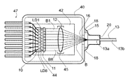
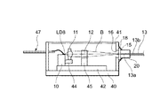
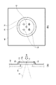
本発明の第1の実施の形態によるレーザモジュールについて説明する。図1および図2は、そのレーザモジュールの概略形状を示す平面図および側断面図である。また、図3(a)および(b)は、パッケージの光出射窓16および光透過部材15の部分の一部拡大側断面図および正面図である。
A laser module according to the first embodiment of the present invention will be described. 1 and 2 are a plan view and a side sectional view showing a schematic shape of the laser module. FIGS. 3A and 3B are a partially enlarged side sectional view and a front view of the
本実施の形態によるレーザモジュールは、図1および図2に示すように、銅または銅合金からなるヒートブロック(放熱ブロック)10上に配列固定された一例として8個のGaN系半導体レーザLD1〜8と、コリメータレンズアレイ11と、集光レンズ12とが、光透過部材15を備えた光出射窓16を有するパッケージ40内に収容され、1本の光ファイバ13がパッケージ40の外部で光透過部材15にその入射端を押しつけるようにして密着固定されてなるものである。
As shown in FIGS. 1 and 2, the laser module according to the present embodiment includes eight GaN-based semiconductor lasers LD1 to LD8 as an example arranged and fixed on a heat block (heat radiation block) 10 made of copper or a copper alloy. The
なおこの図1および2は、本実施の形態のレーザモジュールの基本構成を示すものであり、コリメータレンズアレイ11および集光レンズ12の形状は概略的に示してある。また図の煩雑化を避けるため、GaN系半導体レーザ素子のうち両端に配されている素子LD1およびLD8にのみ符号を付し、またレーザビームB1〜B8のうちB1およびB8にのみ符号を付してある。なお、GaN系半導体レーザLD1〜8は、例えばAlNからなるサブマウント上に固設されたものをヒートブロック10に取付けてもよい。
FIGS. 1 and 2 show the basic configuration of the laser module of the present embodiment, and the shapes of the
これらのGaN系半導体レーザ素子LD1〜8から発散光状態で出射したレーザビームB1〜8は、それぞれレンズアレイ11によって平行光化される。
Laser beams B1 to B8 emitted in a divergent light state from these GaN-based semiconductor laser elements LD1 to LD8 are collimated by the
平行光とされたレーザビームB1〜8は、集光レンズ12によって集光され、図3(a)に示すように光透過部材15の外面15a上で収束するように調芯される。光ファイバ13はその光入射端がフェルール20に挿入されており、光ファイバ13の光入射端が光透過部材15の外面15a上にレーザビーム収束位置に一致するように、フェルール20ごと光透過部材15に密着される。本例ではレンズアレイ11および集光レンズ12によって集光光学系が構成され、それと光ファイバ13とによって合波光学系が構成されている。すなわち、集光レンズ12によって上述のように集光されたレーザビームB1〜8がこの光ファイバ13のコアに入射して光ファイバ13内を伝搬し、1本のレーザビームBに合波されて光ファイバ13の図示しない出射端面から出射する。光ファイバ13は、フェルール20に挿入されている部分を除いて光ファイバ素線13aが樹脂層13bにより被覆されてなるものである。
The parallel laser beams B1 to B8 are collected by the condensing
なお光ファイバ13としては、ステップインデックス型のもの、グレーデッドインデックス型のもの、およびそれらの複合型のものが全て適用可能である。
As the
パッケージ40の底面にはベース板42が固定され、このベース板42の上面にヒートブロック10が取り付けられ、そしてこのヒートブロック10にレンズアレイ11を保持するコリメータレンズホルダ44が固定されている。さらにベース板42の上面には、集光レンズ12を保持する集光レンズホルダ45が固定されている。またGaN系半導体レーザ素子LD1〜8に駆動電流を供給する配線類47は、パッケージ40の光出射窓16が設けられた壁面と対向する横壁面に形成された開口を通してパッケージ外に引き出されている。
A
パッケージ40に設けられている光出射窓16は、例えば、φ6mmの丸穴であり、該光出射窓16に備えられた光透過部材15は、φ10mmの石英ガラスもしくはサファイアからなる円盤状部材であり窓16を覆うようにして取り付けられている。パッケージ40は全面金メッキが施されており、光透過部材15のパッケージ内側面、もしくは内外両面にはARコートが施されている。また、光透過部材15の周縁1mmの部分はメタライズされており、パッケージ40に半田18により取り付けられている。なお、光透過部材15は、円盤状部材に限らず、平行平板、レンズ、楔形等いかなる形状であってもよい。
The
図3(b)は光ファイバ13固定前のパッケージの壁面を同図(a)の矢印P方向から見た正面図である。図3(b)に示すように、光透過部材15にはマーカ19が付されている。このマーカ19は、光透過部材15の外面15a上にエッチングにより形成されたものである。前述のレーザビームの調芯はこのマーカ19を基準としてCCDカメラを用いて調整して行うことができる。
FIG. 3B is a front view of the wall surface of the package before fixing the
次に、本実施形態のレーザモジュールの製造方法について説明する。 Next, a method for manufacturing the laser module of this embodiment will be described.
パッケージ40の上面は開放されて状態で、窓16を覆うように光透過部材15をパッケージ40の壁面に半田18により固定して窓16を封止する。
With the upper surface of the
半導体レーザ素子LD1〜8、コリメータレンズアレイ11および集光レンズ12をパッケージ内部に設置する。この際、レンズアレイ11および集光レンズ12を、複数の半導体レーザ素子LD1〜8から発せられたレーザビームB1〜B8を光透過部材15の外面15a上の所定の位置Oに集光するように、CCDカメラにて光透過部材15の外面15a上のマーカ19を基準として調整を行い、フラックスフリー半田もしくはSi系有機物を含まない接着剤を用い、あるいは融着もしくは溶接により固定する。なお、マーカ19は、直径がファイバのコア径と同等かそれよりわずかに大きいアパーチャであってもよい。
The semiconductor laser elements LD1 to LD8, the
なお、この光透過部材15を取り付ける前に、レンズアレイ11および集光レンズ12を調芯し、その後、光透過部材15を調芯してパッケージ40に固定するようにしてもよい。
Note that the
その後、レーザの長期信頼性を低減させる原因となるパッケージ内部の揮発成分を除去するために、パッケージ40を脱気処理装置に入れて、窒素雰囲気中で90℃に加熱して脱気処理を行う。雰囲気ガスは窒素以外の、例えば酸素、不活性ガスなど、もしくはそれらの混合ガスでもよく、減圧してもよい。脱気処理後、パッケージ40上面に蓋41を設け、フラックスフリー半田もしくはSi系有機物を含まない接着剤を用い、あるいは融着もしくは溶接により封止する。
Thereafter, in order to remove volatile components inside the package, which cause a reduction in long-term reliability of the laser, the
その後、光ファイバ13の入射端を光透過部材15に押し当てて密着させることで、外気を排除して、光ファイバ13の入射端が汚染されないようにする。この状態にて機械的保持、接着、半田固定などにより固定を行う。さらに長期の信頼性を求めるためには、フラックスフリー半田もしくはSi系有機物を含まない接着剤を用い、あるいは融着もしくは溶接により固定を行う。パッケージ内部からのレーザビームBが効率的にファイバコアへ入射するように、パッケージの光透過部材15にファイバ先端が触れない位置にファイバ13を近接した状態にて調芯した後、ファイバ先端を光透過部材15の外面15aに押し当てて固定する。
Thereafter, the incident end of the
このように、本発明のレーザモジュールの製造方法によれば、光ファイバがパッケージに取り付けられる前にパッケージ内の脱気処理を行うことができるので、パッケージ内の脱気処理において光ファイバの樹脂皮膜からの脱ガスによりパッケージ内が汚染されるという虞がない。 As described above, according to the method for manufacturing a laser module of the present invention, since the deaeration process in the package can be performed before the optical fiber is attached to the package, the resin film of the optical fiber is used in the deaeration process in the package. There is no possibility that the inside of the package is contaminated by degassing from the container.
なお、図4にレーザモジュールの他の実施形態の一部拡大側断面図を示すように、パッケージ40の窓16に取り付けられた光透過部材15を覆うようにして、フェルール20と嵌合する装着器(レセプタクル)25が取り付けられていてもよい。レセプタクル25は、予めパッケージ40に備えつけられていてもよいし、パッケージ40の封止後に取り付けてもよい。取り付けは半田18を用いパッケージ内を封止するように行う。レセプタクル25を備えることにより、光ファイバ13のパッケージ40への装着をより簡便なものとすることができる。なお、図4に示すように、レセプタクル40にフェルール20を嵌入し、光ファイバ13の先端を光透過部材15の外面15aに密着させた後に、フェルール20とレセプタクル40を半田42で固定する。なお、フェルール20としては、ジルコニアセラミック、金属、ガラスなどから形成されたものを用いることができる。
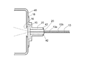
As shown in FIG. 4 which is a partially enlarged side sectional view of another embodiment of the laser module, it is attached to fit the
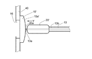
図5にさらに別の実施形態の一部拡大側断面図を示すように、フェルール20の端面20aは光透過部材15’の面15a’に押し当てた際に空気を含まないように、球面研磨したものを使用することが望ましい。このように光ファイバの先端を光透過部材15’の外面15a’に押し当てて密着させることで、外気を排除して入射端が汚染されないようにする。また、光透過部材15’として図5に示すような凸面を有するガラスを用い、該凸面15a’に光ファイバ13先端をY方向に押し当てるようにすれば、密着の際により空気を効果的に排除しつつ密着させることができる。
As shown in a partially enlarged side sectional view of still another embodiment in FIG. 5, spherical polishing is performed so that the
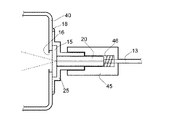
また、さらに別の実施の形態の一部拡大側断面図を図6に示す。図6に示す実施形態のレーザモジュールは、図4と同様にパッケージ40がレセプタクル25を備えているものであり、さらにフェルール20にレセプタクル25と嵌合するコネクタ45を備えたものである。レセプタクル25とフェルール20を半田を用いて固定する代わりに、コネクタ45をレセプタクル25と嵌合させて、フェルール20をレセプタクル25に嵌着させるものである。コネクタ45はバネ46を備えており、フェルール20の後端側からフェルール20を光透過部材15側に押圧する。半田を用いないために、光ファイバ13の取り付けおよび取外しが非常に簡便なものとなる。
Further, FIG. 6 shows a partially enlarged side sectional view of still another embodiment. In the laser module of the embodiment shown in FIG. 6, the
なお、パッケージ40に充填するガスとしては、主として不活性ガスからなるものであることが望ましい。不活性ガスとしては、窒素、希ガスなどが挙げられる。また、不活性ガスと、1ppm以上の酸素、ハロゲン族ガスおよびハロゲン化合物ガスの少なくとも1種類以上とからなる混合ガスであってもよく、例えば、大気と同じ比率の窒素、酸素混合ガスであるクリーンエアを用いてもよい。
Note that the gas filling the
封止雰囲気中に1ppm以上の濃度の酸素が含まれると、レーザモジュールの劣化をより効果的に抑制することができる。このような劣化抑制効果の向上が得られるのは、封止雰囲気中に含有される酸素が、炭化水素成分の光分解により発生した固形物を酸化分解するためである。 When oxygen having a concentration of 1 ppm or more is contained in the sealing atmosphere, deterioration of the laser module can be more effectively suppressed. The reason why such an effect of suppressing deterioration is obtained is that oxygen contained in the sealing atmosphere oxidizes and decomposes solid matter generated by photodecomposition of hydrocarbon components.
ハロゲン族ガスとは、塩素ガス(Cl2)、フッ素ガス(F2)等のハロゲンガスであり、ハロゲン化合物ガスとは、塩素原子(Cl)、臭素原子(Br)、ヨウ素原子(I)、フッ素原子(F)等のハロゲン原子を含有するガス状の化合物である。 The halogen group gas is a halogen gas such as chlorine gas (Cl 2 ), fluorine gas (F 2 ), and the halogen compound gas is a chlorine atom (Cl), bromine atom (Br), iodine atom (I), A gaseous compound containing a halogen atom such as a fluorine atom (F).
ハロゲン化合物ガスとしては、CF3Cl、CF2Cl2、CFCl3、CF3Br、CCl4、CCl4−O2、C2F4Cl2、Cl−H2、CF3Br、PCl3、CF4、SF6、NF3、XeF2、C3F8、CHF3等が挙げられるが、フッ素又は塩素と炭素(C)、窒素(N)、硫黄(S)、キセノン(Xe)との化合物が好ましく、フッ素原子を含有するものが特に好ましい。 Examples of the halogen compound gas include CF 3 Cl, CF 2 Cl 2 , CFCl 3 , CF 3 Br, CCl 4 , CCl 4 —O 2 , C 2 F 4 Cl 2 , Cl—H 2 , CF 3 Br, PCl 3 , CF 4 , SF 6 , NF 3 , XeF 2 , C 3 F 8 , CHF 3 and the like can be mentioned, but fluorine or chlorine and carbon (C), nitrogen (N), sulfur (S), xenon (Xe) Compounds are preferred, and those containing fluorine atoms are particularly preferred.
ハロゲン系ガスは微量でも劣化抑制効果を発揮するが、顕著な劣化抑制効果を得るためには、ハロゲン系ガスの含有濃度を1ppm以上とするのが好ましい。このような劣化抑制効果が得られるのは、封止雰囲気中に含有されるハロゲン系ガスが有機珪素化合物ガスの光分解により発生した堆積物を分解するためである。 Although the halogen-based gas exhibits a deterioration suppressing effect even in a small amount, in order to obtain a remarkable deterioration suppressing effect, it is preferable that the content concentration of the halogen-based gas is 1 ppm or more. Such a deterioration suppressing effect is obtained because the halogen-based gas contained in the sealing atmosphere decomposes the deposit generated by the photodecomposition of the organosilicon compound gas.
また、パッケージ内部におけるレンズアレイ11および集光レンズ12の固定、パッケージの封止の形態としては、上述の通り、フラックスフリー半田もしくはSi系有機物を含まない接着剤を用い、あるいは融着もしくは溶接により固定もしくは封止することにより、より集塵を防止することができる。
In addition, as described above, the
Si系有機物を含まない接着剤としては、例えば、特開2001-177166号公報に記載の脂環式エポキシ化合物、オキセタニル基を有する化合物および触媒量のオニウム塩光反応開始剤を含有する接着性組成物であって、シランカップリング剤を含まない接着性組成物からなるものが挙げられる。 Examples of the adhesive containing no Si-based organic material include an adhesive composition containing an alicyclic epoxy compound described in JP-A-2001-177166, a compound having an oxetanyl group, and a catalytic amount of an onium salt photoreaction initiator. It is a thing and consists of an adhesive composition which does not contain a silane coupling agent.
また、フラックスフリー半田としては、例えば、Sn−Pb、Sn−In、Sn−Pb−In、Au−Sn、Ag−Sn、Sn−Ag−In等が挙げられる。通常の半田材に含まれるフラックスは汚染の要因となるが、フラックスフリーの半田を用いれば汚染物質を発生させる虞がない。なお、環境に配慮して鉛フリー半田を使用することが望ましい。 Examples of the flux-free solder include Sn—Pb, Sn—In, Sn—Pb—In, Au—Sn, Ag—Sn, and Sn—Ag—In. Flux contained in normal solder material causes contamination, but there is no possibility of generating contaminants if flux-free solder is used. In consideration of the environment, it is desirable to use lead-free solder.
溶接は市販のシーム溶接機、例えば日本アビオニクス社製のシーム溶接機を利用して行うことができる。具体的には、パッケージに蓋を載せ、パッケージの蓋と筐体の境界部にシーム溶接機により高電圧を印加することでパッケージの溶接封止を行うことができる。また、融着は市販の融着機、例えば、FITEL S-2000を用いて行うことができる。 Welding can be performed using a commercially available seam welder, for example, a seam welder manufactured by Nippon Avionics. Specifically, the package can be sealed by welding by placing a lid on the package and applying a high voltage to the boundary between the package lid and the housing with a seam welder. The fusion can be performed using a commercially available fusion machine, for example, FITEL S-2000.
次に、上記実施形態において用いられる半導体レーザ素子の一例としてGaN系半導体レーザ素子の製造方法について説明する。図7は、GaN系半導体レーザ素子の製造工程を示す断面図である。 Next, a method for manufacturing a GaN-based semiconductor laser element will be described as an example of the semiconductor laser element used in the above embodiment. FIG. 7 is a cross-sectional view showing the manufacturing process of the GaN-based semiconductor laser device.
図7(a)に示すように、有機金属気相成長法により、トリメチルガリウム(TMG)とアンモニアを成長用原料に用い、n型ドーパントガスとしてシランガスを用い、p型ドーパントとしてシクロペンタジエニルマグネシウム(Cp2Mg)を用い、(0001)C面サファイア基板121上に、温度500℃でGaNバッファ層122を20nm程度の膜厚で形成する。続いて、温度を1050℃にしてGaN層133を2μm程度成長させる。その上に、SiO2膜124を形成し、レジスト125を塗布後、通常のリソグラフィを用いて、
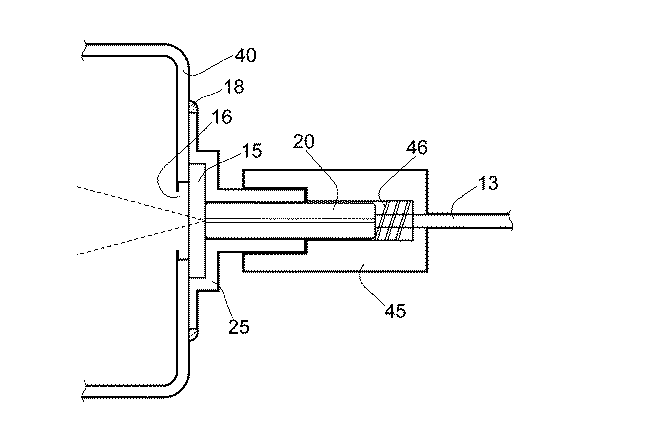
方向に3μm幅のSiO2膜124を除去して、幅7μm程度のSiO2膜124のライン部を形成することにより、10μm程度の周期のラインアンドスペースのパターンを形成する。 By removing the SiO 2 film 124 having a width of 3 μm in the direction to form a line portion of the SiO 2 film 124 having a width of about 7 μm, a line-and-space pattern having a period of about 10 μm is formed.
次に、図7(b)に示すように、レジスト125とSiO2膜124をマスクとして、塩素系のガスを用いてバッファ層122とGaN層123をドライエッチングによりサファイア基板121上面まで除去した後、レジスト125とSiO2膜124を除去する。このとき、サファイア基板121が少しエッチングされてもよい。
Next, as shown in FIG. 7B, after the resist
次に、図7(c)に示すように、GaN層126を20μm程度選択成長させる。この時、横方向の成長により、最終的にストライプが合体して、表面が平坦化する。この時点で、バッファ層122とGaN層123からなる層のライン部上部には貫通転位が発生しているが、そのライン部間のGaN層126には貫通転位は発生していない。
Next, as shown in FIG. 7C, the
次いで、GaN層126上にSiO2膜127を形成し、図7(d)に示すように、前記バッファ層122とGaN層123が残ってできたライン部間のスペース部の中央に位置するSiO2膜127を3μm程除去する。
Next, an SiO 2 film 127 is formed on the
次に、図7(e)に示すように、成長温度を1050℃にしてGaN層128を20μm程度選択成長させる。この時横方向の成長により、最終的にストライプが合体し、表面が平坦化する。
Next, as shown in FIG. 7E, the growth temperature is set to 1050 ° C., and the
次いで、GaN層128上にSiO2膜129を形成し、図7(f)に示すように、残ったSiO2膜127の中央に位置するSiO2膜129を幅3μm程度除去し、その上に、成長温度を1050℃にして、GaN層130を20μm程度選択成長させる。
Next, an SiO 2 film 129 is formed on the
最後に、図7(g)に示すように、上記のように作成したGaN基板上に、n−GaN層131を100〜200μm程度成長させた後、サファイア基板からGaN層130までを除去し、n‐GaN層131を図8に示すn型GaN基板141とする。図8は、半導体レーザ素子の層構成を説明するための、劈開前のウェハの一部の断面図である。
Finally, as shown in FIG. 7G, after the n-
次に、図8に示すように、上記のようにして作製されたn型GaN基板141上に、n−GaNバッファ層142、150ペアのn−Al0.14Ga0.86N(2.5nm)/GaN(2.5nm)超格子クラッド層143、n−GaN光導波層144、n−In0.02Ga0.98N(10.5nm)/n−In0.15Ga0.85N(3.5nm)三重量子井戸活性層145、p−Al0.2Ga0.8Nキャリアブロック層146、p−GaN光導波層147、150ペアのp−Al0.14Ga0.86N(2.5nm)/GaN(2.5nm)超格子クラッド層148、p−GaNコンタクト層149を積層する。ここでは、p型の不純物としてMgを使用する。このMgの活性化のために成長後窒素雰囲気中で熱処理するか、または窒素リッチ雰囲気で成長を実施するかのいずれかの方法を用いてもよい。
Next, as shown in FIG. 8, the n-
次に、横シングルモード半導体レーザを作製する場合は、横モードがシングルとなるストライプ領域を形成するために幅1〜3μmのストライプ状開口を有するSiO2マスク150を100〜500μmピッチで形成し、横マルチモードのブロード半導体レーザを作成する場合は、幅数〜50μmのストライプ状の開口を有するSiO2マスク150を100〜500μmピッチで形成する。数〜50μmの幅のストライプ領域を有する横マルチモードのブロード半導体レーザからは数百〜2000mW程度の出力が得られる。 Next, when fabricating a lateral single mode semiconductor laser, in order to form a stripe region in which the transverse mode is single, a SiO 2 mask 150 having a stripe-shaped opening having a width of 1 to 3 μm is formed at a pitch of 100 to 500 μm. In the case of producing a horizontal multimode broad semiconductor laser, SiO 2 masks 150 having stripe-shaped openings with a width of several to 50 μm are formed at a pitch of 100 to 500 μm. An output of about several hundred to 2,000 mW can be obtained from a lateral multimode broad semiconductor laser having a stripe region with a width of several to 50 μm.
次に、ストライプ状の開口を覆うようにしてNi/Auよりなるストライプ状のp電極151を形成する。次に、基板141を研磨し、Ti/Auよりなるn電極152を形成し、劈開して形成した共振器面に高反射コート、低反射コートを行い、その後、さらに劈開して所望の数のキャビティ、共振器長を有する半導体レーザ素子LDを完成させる。
Next, a striped p-
マルチキャビティの半導体レーザ素子とする場合には、共振器長100〜1500μm好ましくは400μmとなり、発光点配列方向の長さが例えば1cmとなるように劈開し、キャビティ面に高反射、低反射コートを行い、例えば、20個のキャビティを有するバー状の素子を完成させる。なお、マルチキャビティを形成する場合は、必要キャビティ数に応じて発光点配列方向の素子幅にて劈開を実施し、素子形成する。 In the case of a multi-cavity semiconductor laser device, the cavity length is 100 to 1500 μm, preferably 400 μm, and the length in the direction of the emission point arrangement is cleaved to 1 cm, for example, and the cavity surface is coated with a high reflection and low reflection coating. For example, a bar-shaped element having 20 cavities is completed. In the case of forming a multi-cavity, the element is formed by cleaving with the element width in the light emitting point arrangement direction according to the required number of cavities.
シングルキャビティの半導体レーザ素子を形成する場合は、ストライプ領域の形成ピッチと同等の100〜500μmピッチで劈開し、シングルキャビティを有する共振器長400μmの素子とする。 In the case of forming a single cavity semiconductor laser element, an element having a cavity length of 400 μm having a single cavity is formed by cleaving at a pitch of 100 to 500 μm, which is equal to the formation pitch of the stripe region.
なお、本発明のレーザモジュールにおいてパッケージ内に収容される半導体レーザ素子の形態としては、上記実施形態に示したディスクリートなシングルキャビティチップをアレイ状に配置したもののほか、1つのマルチキャビティ半導体レーザ素子(LDバー)、複数のマルチキャビティ半導体レーザ素子をアレイ状に配置したもの、あるいはシングルキャビティ半導体レーザ素子とマルチキャビティ半導体レーザ素子の組み合わせなどであってもよい。 In addition, as a form of the semiconductor laser element accommodated in the package in the laser module of the present invention, one multicavity semiconductor laser element (in addition to the discrete single cavity chip shown in the above embodiment arranged in an array) LD bar), a plurality of multi-cavity semiconductor laser elements arranged in an array, or a combination of a single-cavity semiconductor laser element and a multi-cavity semiconductor laser element.
図9は、本発明の第2の実施形態のレーザモジュールの平面図を示すものである。 FIG. 9 is a plan view of a laser module according to the second embodiment of the present invention.
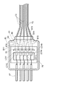
本実施の形態によるレーザモジュールは、ヒートブロック70上に配列固定された5個のチップ状態のシングルキャビティGaN系半導体レーザLD11〜15と、集光レンズアレイ72とが、光透過部材85を備えた光出射窓86を有するパッケージ80内に収容され、5本の光ファイバ73がパッケージ80の外部で光透過部材85にその入射端を押しつけるようにして密着固定されてなるものである。このレーザモジュールは、ファイバアレイ型のレーザモジュールであり、半導体レーザ素子から出射されたレーザビームをそれぞれ異なる光ファイバに結合させるものである。
In the laser module according to the present embodiment, five chip-state single-cavity GaN-based
GaN系半導体レーザ素子LD11〜15から発散光状態で出射したレーザビームB11〜15は、それぞれ集光レンズアレイ72を構成する各集光レンズによって集光されてそれぞれ光透過部材85の外面上の異なる位置に収束される。5本の光ファイバ73はマルチファイバフェルール90にその先端が挿入され、各レーザビームB11〜15の収束位置に入射端が密着固定される。各レーザビームB11〜15はそれぞれ異なる光ファイバ73に結合して、各光ファイバ73の図示しない出射端から出射される。
Laser beams B11-15 emitted from the GaN-based semiconductor laser elements LD11-15 in a divergent state are condensed by the respective condensing lenses constituting the condensing
本実施形態のレーザモジュールにおいても、パッケージ80は脱気処理後に気密封止されており、各部材の固定およびパッケージ封止は、フラックスフリー半田もしくはSi系有機物を含まない接着剤を用いて、あるいは融着もしくは溶接により行われている。したがって、パッケージ80内部において、光密度の高い半導体レーザ素子の光出射端面への集塵は抑制され、また、光透過部材85のパッケージの内側面はレーザビームの集光点ではないために、光密度が低く該面における集塵効果が抑制される。また、光ファイバ73の入射端は光透過部材85に密着されているので大気に触れることがなく汚染されない。レーザモジュール全体として集塵効果が抑制されるので光出力を向上させることができ、また高い信頼性を得ることができる。
Also in the laser module of the present embodiment, the
図10は、本発明の第3の実施形態のレーザモジュールの平面図を示すものである。 FIG. 10 is a plan view of a laser module according to the third embodiment of the present invention.
本実施形態のレーザモジュールは、GaN系半導体レーザ素子LDを内部に備え、気密封止されたCANパッケージ110と、集光レンズ12とが、光透過部材15を備えた光出射窓16を有するパッケージ40内に収容され、1本の光ファイバ13がパッケージ40の外部で光透過部材15にその入射端を押しつけるようにして密着固定されてなるものである。ここでは、第1の実施形態のレーザモジュールと同等の要素には同符号を付し詳細な説明を省略する。
The laser module of this embodiment includes a GaN-based semiconductor laser element LD inside, a hermetically sealed
CANパッケージ110、集光レンズ12はベース板105上の各固定部材に、半導体レーザ素子LDから出射されたレーザビームBが集光レンズ12により光透過部材15の外面15a上で収束するように配置固定されている。それぞれの固定には、フラックスフリー半田もしくはSi系有機物を含まない接着剤が用いられている。なお、融着もしくは溶接により固定されてもよい。
The
本実施形態においては、半導体レーザ素子LDが、CANパッケージ110中に備えられている。CANパッケージは、内部の揮発成分を除去するため脱気処理を施した上で気密封止されたものである。半導体レーザ素子LDは、脱気処理され気密封止されたCANパッケージ110内に備えられており、CANパッケージ110の脱気処理時には、光ファイバ13を脱気処理装置内に配することはないので、光ファイバ13の樹脂皮膜からの脱ガスによる影響を受けない。さらに、このCANパッケージ110は気密封止されたパッケージ40の内部に備えられているため、集塵効果をより抑制することができ、レーザモジュール全体として集塵効果が抑制されるので光出力を向上させることができ、また高い信頼性を得ることができる。特に上述の製造方法により製造されるGaN系半導体レーザ素子のような発振波長400nm帯の高出力半導体レーザ素子を備えた場合には、集塵効果が顕著であるため、本実施形態のように半導体レーザ素子を2重にパッケージで内包した構造とする効果が大きい。
In the present embodiment, the semiconductor laser element LD is provided in the
なお、パッケージ内に収容される半導体レーザ素子の形態としては、上記実施形態に示したディスクリートなシングルキャビティチップをアレイ状に配置したもののほか、1つのマルチキャビティ半導体レーザ素子(LDバー)、複数のマルチキャビティ半導体レーザ素子をアレイ状に配置したもの、あるいはシングルキャビティ半導体レーザ素子とマルチキャビティ半導体レーザ素子の組み合わせなどであってもよい。 The semiconductor laser element accommodated in the package includes one multi-cavity semiconductor laser element (LD bar), a plurality of discrete single-cavity chips arranged in an array, as shown in the above embodiment, and a plurality of semiconductor laser elements. It may be a multi-cavity semiconductor laser element arranged in an array, or a combination of a single-cavity semiconductor laser element and a multi-cavity semiconductor laser element.
LD,LD1〜8 半導体レーザ素子
B,B1〜8 レーザビーム
10 ヒートブロック
11 レンズアレイ
12 集光レンズ
13 光ファイバ
13a 光ファイバ素線
13b 樹脂被膜
15 光透過部材
16 光出射窓
18 半田
20 フェルール
25 レセプタクル
40 パッケージ
LD, LD1-8 Semiconductor laser element B, B1-8 Laser beam
10 Heat block
11 Lens array
12 Condensing lens
13 Optical fiber
13a Optical fiber
13b Resin coating
15 Light transmissive member
16 Light exit window
18 Solder
20 Ferrule
25 Receptacle
40 packages
Claims (9)
前記パッケージの内部に配置された1つもしくは複数の半導体レーザ素子と、
前記パッケージの外部に配置された光ファイバと、
前記半導体レーザ素子から出射されたレーザビームを前記光透過部材の外面上に集光させる、前記パッケージの内部に配置された集光光学系とを備え、
前記光ファイバの入射端が、前記光透過部材の外面の、前記レーザビームが集光する位置に密着して固定されていることを特徴とするレーザモジュール。 A hermetically sealed package with a light transmissive member in the light exit window;
One or more semiconductor laser elements disposed inside the package;
An optical fiber disposed outside the package;
A condensing optical system disposed inside the package for condensing a laser beam emitted from the semiconductor laser element on an outer surface of the light transmitting member;
An incident end of the optical fiber is fixed in close contact with a position on the outer surface of the light transmitting member where the laser beam is condensed.
前記パッケージが、前記フェルールと嵌合する装着器を備えていることを特徴とする請求項1から3いずれか1項記載のレーザモジュール。 The incident end of the optical fiber is inserted into the ferrule,
4. The laser module according to claim 1, wherein the package includes a mounting device that fits with the ferrule. 5.
一壁面に前記レーザビームが透過する光透過部材を備えた光出射窓を有する、気密封止可能なパッケージの内部に、前記半導体レーザ素子と前記集光光学系を、前記レーザビームが前記光透過部材の外面上に集光されるように配置し、
前記パッケージの内部を脱気処理し、
該脱気処理後、前記パッケージを気密封止し、
その後、前記光ファイバの入射端に前記レーザビームが光学的に結合するように、該光ファイバの入射端を前記光透過部材の前記外面に密着させて固定することを特徴とするレーザモジュールの製造方法。 Manufacturing of a laser module comprising one or a plurality of semiconductor laser elements, an optical fiber, and a condensing optical system for condensing a laser beam emitted from the semiconductor laser element and coupling it to an incident end of the optical fiber In the method
The semiconductor laser element and the condensing optical system are disposed in a hermetically sealable package having a light exit window provided with a light transmitting member through which the laser beam is transmitted on one wall surface, and the laser beam transmits the light. Place it so that it is focused on the outer surface of the member,
Degassing the inside of the package;
After the deaeration treatment, the package is hermetically sealed,
Thereafter, the laser light beam is optically coupled to the incident end of the optical fiber so that the incident end of the optical fiber is fixed in contact with the outer surface of the light transmitting member. Method.
Priority Applications (1)
| Application Number | Priority Date | Filing Date | Title |
|---|---|---|---|
| JP2003433527A JP2004252425A (en) | 2003-01-31 | 2003-12-26 | Laser module and manufacturing method therefor |
Applications Claiming Priority (2)
| Application Number | Priority Date | Filing Date | Title |
|---|---|---|---|
| JP2003024997 | 2003-01-31 | ||
| JP2003433527A JP2004252425A (en) | 2003-01-31 | 2003-12-26 | Laser module and manufacturing method therefor |
Publications (1)
| Publication Number | Publication Date |
|---|---|
| JP2004252425A true JP2004252425A (en) | 2004-09-09 |
Family
ID=33032313
Family Applications (1)
| Application Number | Title | Priority Date | Filing Date |
|---|---|---|---|
| JP2003433527A Pending JP2004252425A (en) | 2003-01-31 | 2003-12-26 | Laser module and manufacturing method therefor |
Country Status (1)
| Country | Link |
|---|---|
| JP (1) | JP2004252425A (en) |
Cited By (15)
| Publication number | Priority date | Publication date | Assignee | Title |
|---|---|---|---|---|
| WO2005119862A1 (en) * | 2004-06-02 | 2005-12-15 | Matsushita Electric Industrial Co., Ltd. | Semiconductor laser device and method for fabricating same |
| WO2006098267A1 (en) * | 2005-03-14 | 2006-09-21 | Matsushita Electric Industrial Co., Ltd. | Semiconductor laser, optical pickup and optical information processing device |
| EP1712939A1 (en) * | 2005-04-12 | 2006-10-18 | ILTI LUCE S.r.l. | Light emitting diode lighting assembly particularly for optical fibres |
| JP2006286866A (en) * | 2005-03-31 | 2006-10-19 | Fuji Photo Film Co Ltd | Laser module |
| JP2007019470A (en) * | 2005-06-08 | 2007-01-25 | Sharp Corp | Laser device manufacturing method |
| US7254298B2 (en) | 2005-03-31 | 2007-08-07 | Fujifilm Corporation | Light source module |
| US7436875B2 (en) | 2005-07-20 | 2008-10-14 | Fujifilm Corporation | Laser module having controlled optical power density at exposed surfaces |
| US7656916B2 (en) | 2006-12-22 | 2010-02-02 | Sharp Kabushiki Kaisha | Semiconductor light emitting device and method for fabricating same |
| JP2014187407A (en) * | 2009-08-18 | 2014-10-02 | Mitsubishi Electric Corp | Light source device, and method of manufacturing light source device |
| JP2015043028A (en) * | 2013-08-26 | 2015-03-05 | 三菱電機株式会社 | Apparatus and method for manufacturing integrated optical module |
| JP2018067576A (en) * | 2016-10-17 | 2018-04-26 | ファナック株式会社 | Laser oscillator |
| JP2019508081A (en) * | 2015-12-16 | 2019-03-28 | コミサリア ア エナジー アトミック エ オックス エナジーズ オルタネティヴ | Device for optical stimulation of the brain via an optical fiber |
| US10431959B2 (en) | 2017-10-02 | 2019-10-01 | Nichia Corporation | Light emitting device and optical device |
| JP2019176046A (en) * | 2018-03-29 | 2019-10-10 | 株式会社島津製作所 | Underwater laser light source |
| US11476639B2 (en) | 2018-09-13 | 2022-10-18 | Panasonic Holdings Corporation | Optical apparatus |
-
2003
- 2003-12-26 JP JP2003433527A patent/JP2004252425A/en active Pending
Cited By (26)
| Publication number | Priority date | Publication date | Assignee | Title |
|---|---|---|---|---|
| WO2005119862A1 (en) * | 2004-06-02 | 2005-12-15 | Matsushita Electric Industrial Co., Ltd. | Semiconductor laser device and method for fabricating same |
| JPWO2005119862A1 (en) * | 2004-06-02 | 2008-04-03 | 松下電器産業株式会社 | Semiconductor laser device and manufacturing method thereof |
| US7653099B2 (en) | 2004-06-02 | 2010-01-26 | Panasonic Corporation | Semiconductor laser device which is capable of stably emitting short-wavelength laser light |
| JP5036308B2 (en) * | 2004-06-02 | 2012-09-26 | パナソニック株式会社 | Semiconductor laser device and manufacturing method thereof |
| WO2006098267A1 (en) * | 2005-03-14 | 2006-09-21 | Matsushita Electric Industrial Co., Ltd. | Semiconductor laser, optical pickup and optical information processing device |
| JP2006286866A (en) * | 2005-03-31 | 2006-10-19 | Fuji Photo Film Co Ltd | Laser module |
| US7254298B2 (en) | 2005-03-31 | 2007-08-07 | Fujifilm Corporation | Light source module |
| US7572068B2 (en) | 2005-03-31 | 2009-08-11 | Fujifilm Corporation | Laser module having detachable transparent member covering light-output window |
| EP1712939A1 (en) * | 2005-04-12 | 2006-10-18 | ILTI LUCE S.r.l. | Light emitting diode lighting assembly particularly for optical fibres |
| JP2007019470A (en) * | 2005-06-08 | 2007-01-25 | Sharp Corp | Laser device manufacturing method |
| US7436875B2 (en) | 2005-07-20 | 2008-10-14 | Fujifilm Corporation | Laser module having controlled optical power density at exposed surfaces |
| US7656916B2 (en) | 2006-12-22 | 2010-02-02 | Sharp Kabushiki Kaisha | Semiconductor light emitting device and method for fabricating same |
| JP2014187407A (en) * | 2009-08-18 | 2014-10-02 | Mitsubishi Electric Corp | Light source device, and method of manufacturing light source device |
| JP2015043028A (en) * | 2013-08-26 | 2015-03-05 | 三菱電機株式会社 | Apparatus and method for manufacturing integrated optical module |
| JP2019508081A (en) * | 2015-12-16 | 2019-03-28 | コミサリア ア エナジー アトミック エ オックス エナジーズ オルタネティヴ | Device for optical stimulation of the brain via an optical fiber |
| US11202922B2 (en) | 2015-12-16 | 2021-12-21 | Commissariat à l'Energie Atomique et aux Energies Alternatives | Device for optically stimulating the brain via an optical fiber |
| JP2018067576A (en) * | 2016-10-17 | 2018-04-26 | ファナック株式会社 | Laser oscillator |
| US10186834B2 (en) | 2016-10-17 | 2019-01-22 | Fanuc Corporation | Laser oscillator |
| US10770866B2 (en) | 2017-10-02 | 2020-09-08 | Nichia Corporation | Light emitting device |
| US10431959B2 (en) | 2017-10-02 | 2019-10-01 | Nichia Corporation | Light emitting device and optical device |
| US11271372B2 (en) | 2017-10-02 | 2022-03-08 | Nichia Corporation | Optical apparatus |
| US11710943B2 (en) | 2017-10-02 | 2023-07-25 | Nichia Corporation | Light emitting device |
| JP2019176046A (en) * | 2018-03-29 | 2019-10-10 | 株式会社島津製作所 | Underwater laser light source |
| JP7114984B2 (en) | 2018-03-29 | 2022-08-09 | 株式会社島津製作所 | Underwater laser light source |
| US11476639B2 (en) | 2018-09-13 | 2022-10-18 | Panasonic Holdings Corporation | Optical apparatus |
| US11894653B2 (en) | 2018-09-13 | 2024-02-06 | Panasonic Holdings Corporation | Optical apparatus |
Similar Documents
| Publication | Publication Date | Title |
|---|---|---|
| JP2004253783A (en) | Laser module | |
| US7110425B2 (en) | Laser module and production process thereof | |
| US7226222B2 (en) | Laser module with sealed packages having reduced total volume | |
| JP2006066875A (en) | Laser module | |
| CN100583576C (en) | Laser module and its manufacturing method | |
| US20040184753A1 (en) | Fiber module in which optical fiber coated with metal or inorganic material is fixed to sealable package so that an end of the optical fiber appears inside the package | |
| JP4129135B2 (en) | Semiconductor package | |
| JP2004233885A (en) | Laser module and its manufacture method | |
| JP2006286866A (en) | Laser module | |
| JP4274409B2 (en) | Laser equipment | |
| JP4084068B2 (en) | Laser module | |
| US7790484B2 (en) | Method for manufacturing laser devices | |
| KR101014148B1 (en) | Assembly method of light emitting device | |
| US8441029B2 (en) | Light emitting element including side surface dielectric layer for avoiding impurity adhesion | |
| CN100420110C (en) | Method of manufacturing laser device | |
| KR20040070094A (en) | Laser module | |
| JP2004235534A (en) | Laser element and manufacturing method thereof, and laser module using the laser element | |
| JP2004126001A (en) | Laser apparatus | |
| JP4740030B2 (en) | Laser device manufacturing method | |
| JP4557133B2 (en) | Semiconductor optical device | |
| JP2004179595A (en) | Optical recording device | |
| JP2007073830A (en) | Semiconductor laser device and optical module | |
| JP2020129653A (en) | Light emitting device and manufacturing method thereof | |
| KR20080094152A (en) | Semiconductor laser diodes and their packages |
Legal Events
| Date | Code | Title | Description |
|---|---|---|---|
| A621 | Written request for application examination |
Free format text: JAPANESE INTERMEDIATE CODE: A621 Effective date: 20060428 |
|
| A711 | Notification of change in applicant |
Free format text: JAPANESE INTERMEDIATE CODE: A712 Effective date: 20061207 |
|
| A977 | Report on retrieval |
Free format text: JAPANESE INTERMEDIATE CODE: A971007 Effective date: 20080403 |
|
| A131 | Notification of reasons for refusal |
Free format text: JAPANESE INTERMEDIATE CODE: A131 Effective date: 20080610 |
|
| A131 | Notification of reasons for refusal |
Free format text: JAPANESE INTERMEDIATE CODE: A131 Effective date: 20080902 |
|
| A02 | Decision of refusal |
Free format text: JAPANESE INTERMEDIATE CODE: A02 Effective date: 20090106 |