JP2004256902A - Cu-Cr-Zr ALLOY, AND PRODUCTION METHOD THEREFOR - Google Patents
Cu-Cr-Zr ALLOY, AND PRODUCTION METHOD THEREFOR Download PDFInfo
- Publication number
- JP2004256902A JP2004256902A JP2003051833A JP2003051833A JP2004256902A JP 2004256902 A JP2004256902 A JP 2004256902A JP 2003051833 A JP2003051833 A JP 2003051833A JP 2003051833 A JP2003051833 A JP 2003051833A JP 2004256902 A JP2004256902 A JP 2004256902A
- Authority
- JP
- Japan
- Prior art keywords
- alloy
- less
- oxide film
- aging
- mpa
- Prior art date
- Legal status (The legal status is an assumption and is not a legal conclusion. Google has not performed a legal analysis and makes no representation as to the accuracy of the status listed.)
- Pending
Links
- 229910045601 alloy Inorganic materials 0.000 title claims abstract description 69
- 239000000956 alloy Substances 0.000 title claims abstract description 69
- 229910017526 Cu-Cr-Zr Inorganic materials 0.000 title claims abstract description 58
- 229910017810 Cu—Cr—Zr Inorganic materials 0.000 title claims abstract description 58
- 238000004519 manufacturing process Methods 0.000 title claims description 41
- 239000010949 copper Substances 0.000 claims abstract description 39
- RYGMFSIKBFXOCR-UHFFFAOYSA-N Copper Chemical compound [Cu] RYGMFSIKBFXOCR-UHFFFAOYSA-N 0.000 claims abstract description 6
- 229910052802 copper Inorganic materials 0.000 claims abstract description 6
- 239000012535 impurity Substances 0.000 claims abstract description 5
- 238000005498 polishing Methods 0.000 claims description 76
- 230000032683 aging Effects 0.000 claims description 73
- 230000035882 stress Effects 0.000 claims description 72
- 238000011282 treatment Methods 0.000 claims description 55
- 239000000126 substance Substances 0.000 claims description 39
- 238000007747 plating Methods 0.000 claims description 26
- 238000000137 annealing Methods 0.000 claims description 20
- 238000005097 cold rolling Methods 0.000 claims description 12
- 239000001257 hydrogen Substances 0.000 claims description 11
- 229910052739 hydrogen Inorganic materials 0.000 claims description 11
- UFHFLCQGNIYNRP-UHFFFAOYSA-N Hydrogen Chemical compound [H][H] UFHFLCQGNIYNRP-UHFFFAOYSA-N 0.000 claims description 10
- 239000011261 inert gas Substances 0.000 claims description 7
- 229910052718 tin Inorganic materials 0.000 claims description 7
- 229910052738 indium Inorganic materials 0.000 claims description 6
- 229910052749 magnesium Inorganic materials 0.000 claims description 6
- 229910052748 manganese Inorganic materials 0.000 claims description 6
- 229910052698 phosphorus Inorganic materials 0.000 claims description 6
- 229910052742 iron Inorganic materials 0.000 claims description 5
- 229910052759 nickel Inorganic materials 0.000 claims description 5
- 229910052710 silicon Inorganic materials 0.000 claims description 5
- 229910052719 titanium Inorganic materials 0.000 claims description 4
- 229910019580 Cr Zr Inorganic materials 0.000 claims 1
- 229910019817 Cr—Zr Inorganic materials 0.000 claims 1
- 229910000679 solder Inorganic materials 0.000 abstract description 29
- 229910052726 zirconium Inorganic materials 0.000 abstract description 5
- 229910052804 chromium Inorganic materials 0.000 abstract description 4
- 239000000463 material Substances 0.000 description 33
- 230000000052 comparative effect Effects 0.000 description 19
- 239000000243 solution Substances 0.000 description 14
- 230000000694 effects Effects 0.000 description 13
- 238000011156 evaluation Methods 0.000 description 13
- 230000007423 decrease Effects 0.000 description 12
- 239000011651 chromium Substances 0.000 description 11
- 238000000034 method Methods 0.000 description 9
- 229910000881 Cu alloy Inorganic materials 0.000 description 7
- QAOWNCQODCNURD-UHFFFAOYSA-N Sulfuric acid Chemical compound OS(O)(=O)=O QAOWNCQODCNURD-UHFFFAOYSA-N 0.000 description 6
- 230000015572 biosynthetic process Effects 0.000 description 6
- 238000005096 rolling process Methods 0.000 description 6
- 239000011701 zinc Substances 0.000 description 6
- PXHVJJICTQNCMI-UHFFFAOYSA-N nickel Substances [Ni] PXHVJJICTQNCMI-UHFFFAOYSA-N 0.000 description 5
- 238000001556 precipitation Methods 0.000 description 5
- 239000006104 solid solution Substances 0.000 description 5
- 238000004544 sputter deposition Methods 0.000 description 5
- XLYOFNOQVPJJNP-UHFFFAOYSA-N water Chemical compound O XLYOFNOQVPJJNP-UHFFFAOYSA-N 0.000 description 5
- XKRFYHLGVUSROY-UHFFFAOYSA-N Argon Chemical compound [Ar] XKRFYHLGVUSROY-UHFFFAOYSA-N 0.000 description 4
- IJGRMHOSHXDMSA-UHFFFAOYSA-N Atomic nitrogen Chemical compound N#N IJGRMHOSHXDMSA-UHFFFAOYSA-N 0.000 description 4
- MHAJPDPJQMAIIY-UHFFFAOYSA-N Hydrogen peroxide Chemical compound OO MHAJPDPJQMAIIY-UHFFFAOYSA-N 0.000 description 4
- 238000005259 measurement Methods 0.000 description 4
- 239000002244 precipitate Substances 0.000 description 4
- 238000004381 surface treatment Methods 0.000 description 4
- 230000009471 action Effects 0.000 description 3
- QVGXLLKOCUKJST-UHFFFAOYSA-N atomic oxygen Chemical compound [O] QVGXLLKOCUKJST-UHFFFAOYSA-N 0.000 description 3
- 150000001875 compounds Chemical class 0.000 description 3
- 238000002845 discoloration Methods 0.000 description 3
- 239000007789 gas Substances 0.000 description 3
- 238000007654 immersion Methods 0.000 description 3
- 239000007788 liquid Substances 0.000 description 3
- 239000001301 oxygen Substances 0.000 description 3
- 229910052760 oxygen Inorganic materials 0.000 description 3
- 230000008569 process Effects 0.000 description 3
- 238000012360 testing method Methods 0.000 description 3
- 239000013585 weight reducing agent Substances 0.000 description 3
- CSCPPACGZOOCGX-UHFFFAOYSA-N Acetone Chemical compound CC(C)=O CSCPPACGZOOCGX-UHFFFAOYSA-N 0.000 description 2
- 229910001369 Brass Inorganic materials 0.000 description 2
- 229910000906 Bronze Inorganic materials 0.000 description 2
- KRHYYFGTRYWZRS-UHFFFAOYSA-N Fluorane Chemical compound F KRHYYFGTRYWZRS-UHFFFAOYSA-N 0.000 description 2
- OAICVXFJPJFONN-UHFFFAOYSA-N Phosphorus Chemical compound [P] OAICVXFJPJFONN-UHFFFAOYSA-N 0.000 description 2
- 238000003483 aging Methods 0.000 description 2
- 229910052786 argon Inorganic materials 0.000 description 2
- 238000005452 bending Methods 0.000 description 2
- 239000010951 brass Substances 0.000 description 2
- 239000010974 bronze Substances 0.000 description 2
- 230000008859 change Effects 0.000 description 2
- 238000001816 cooling Methods 0.000 description 2
- KUNSUQLRTQLHQQ-UHFFFAOYSA-N copper tin Chemical compound [Cu].[Sn] KUNSUQLRTQLHQQ-UHFFFAOYSA-N 0.000 description 2
- 230000007797 corrosion Effects 0.000 description 2
- 238000005260 corrosion Methods 0.000 description 2
- 238000010586 diagram Methods 0.000 description 2
- 239000010419 fine particle Substances 0.000 description 2
- 238000010438 heat treatment Methods 0.000 description 2
- 229910000765 intermetallic Inorganic materials 0.000 description 2
- 229910052757 nitrogen Inorganic materials 0.000 description 2
- 238000007517 polishing process Methods 0.000 description 2
- 230000001376 precipitating effect Effects 0.000 description 2
- 238000012545 processing Methods 0.000 description 2
- 239000002994 raw material Substances 0.000 description 2
- 238000009736 wetting Methods 0.000 description 2
- 229910052725 zinc Inorganic materials 0.000 description 2
- 238000002441 X-ray diffraction Methods 0.000 description 1
- HCHKCACWOHOZIP-UHFFFAOYSA-N Zinc Chemical compound [Zn] HCHKCACWOHOZIP-UHFFFAOYSA-N 0.000 description 1
- GXDVEXJTVGRLNW-UHFFFAOYSA-N [Cr].[Cu] Chemical compound [Cr].[Cu] GXDVEXJTVGRLNW-UHFFFAOYSA-N 0.000 description 1
- 239000002253 acid Substances 0.000 description 1
- 150000007513 acids Chemical class 0.000 description 1
- 239000007864 aqueous solution Substances 0.000 description 1
- 239000011248 coating agent Substances 0.000 description 1
- 238000000576 coating method Methods 0.000 description 1
- 229910052681 coesite Inorganic materials 0.000 description 1
- 229910000365 copper sulfate Inorganic materials 0.000 description 1
- XTYUEDCPRIMJNG-UHFFFAOYSA-N copper zirconium Chemical compound [Cu].[Zr] XTYUEDCPRIMJNG-UHFFFAOYSA-N 0.000 description 1
- ARUVKPQLZAKDPS-UHFFFAOYSA-L copper(II) sulfate Chemical compound [Cu+2].[O-][S+2]([O-])([O-])[O-] ARUVKPQLZAKDPS-UHFFFAOYSA-L 0.000 description 1
- 229910052906 cristobalite Inorganic materials 0.000 description 1
- 230000007547 defect Effects 0.000 description 1
- 238000013461 design Methods 0.000 description 1
- 238000011161 development Methods 0.000 description 1
- 230000018109 developmental process Effects 0.000 description 1
- 230000004907 flux Effects 0.000 description 1
- 150000002431 hydrogen Chemical class 0.000 description 1
- 230000006872 improvement Effects 0.000 description 1
- 239000011159 matrix material Substances 0.000 description 1
- 238000002844 melting Methods 0.000 description 1
- 230000008018 melting Effects 0.000 description 1
- 229910052751 metal Inorganic materials 0.000 description 1
- 239000002184 metal Substances 0.000 description 1
- 238000002156 mixing Methods 0.000 description 1
- 239000000203 mixture Substances 0.000 description 1
- MOFOBJHOKRNACT-UHFFFAOYSA-N nickel silver Chemical compound [Ni].[Ag] MOFOBJHOKRNACT-UHFFFAOYSA-N 0.000 description 1
- 239000010956 nickel silver Substances 0.000 description 1
- 230000003647 oxidation Effects 0.000 description 1
- 238000007254 oxidation reaction Methods 0.000 description 1
- 238000005554 pickling Methods 0.000 description 1
- 230000009467 reduction Effects 0.000 description 1
- 238000000682 scanning probe acoustic microscopy Methods 0.000 description 1
- 239000000377 silicon dioxide Substances 0.000 description 1
- VYPSYNLAJGMNEJ-UHFFFAOYSA-N silicon dioxide Inorganic materials O=[Si]=O VYPSYNLAJGMNEJ-UHFFFAOYSA-N 0.000 description 1
- 229910052682 stishovite Inorganic materials 0.000 description 1
- 238000005482 strain hardening Methods 0.000 description 1
- 238000005728 strengthening Methods 0.000 description 1
- 238000010301 surface-oxidation reaction Methods 0.000 description 1
- 238000010998 test method Methods 0.000 description 1
- 229910052905 tridymite Inorganic materials 0.000 description 1
Images


Landscapes
- Conductive Materials (AREA)
Abstract
Description
【0001】
【発明の属する技術分野】
本発明は、各種端子、コネクタ、リレーまたはスイッチなどの電子部品の製造に使用するCu−Cr−Zr合金およびその製造方法に係り、特に、ばね性およびはんだ濡れ性とを高いレベルで同時に実現したCu−Cr−Zr合金の製造技術に関するものである。
【0002】
【従来の技術】
従来、電子機器の各種端子、コネクタ、リレーまたはスイッチなどの電気導電性およびばね性が必要な材料においては、製造コストを重視する用途には低廉な黄銅が適用されていた。また、ばね性が重視される用途にはりん青銅が適用されていた。さらに、ばね性および耐食性が重視される用途には洋白が適用されていた。しかしながら、近年における電子機器類およびその部品の軽量化、薄肉化および小型化に伴い、これらの材料を使用したのでは必要強度を十分に満足することができないのが現状である。また、これらの材料は電気伝導度の点では必ずしも満足できるとは言えず、またコネクターとしての性能面からは「接触部において応力緩和特性が悪い」という欠点が指摘されていた。
【0003】
近年電子機器の各種端子、コネクタ、リレーまたはスイッチなどの電気導電性およびばね性が必要な材料においては、従来のりん青銅、黄銅などに代表される固溶強化型合金に代わり、高強度及び高導電性の観点から、時効硬化型の銅合金の使用量が増加している。時効硬化型の銅合金は、溶体化処理された過飽和固溶体を時効処理することにより、微細粒子が均一に析出して耐力やばね限界値などの強度特性の向上と共に固溶元素量が減少し導電率の向上に寄与する。
【0004】
従って、益々厳しくなる電子機器類およびその部品の軽量化、材料の高強度化の要求を満足する材料として、時効硬化型の銅合金が使用されている。時効硬化型銅合金のうち、Cu−Cr−Zr系銅合金は高強度と高導電率を併せ持つ代表的な銅合金である。Cu−Cr−Zr合金のCr、Zrは活性な元素であり、合金の特性を改良する目的で活性金属を更に添加する場合もある。この銅合金では、Crは単体で、またZrはCuと化合物を形成し母材中に析出して、強度と導電率が上昇し、曲げ加工性および応力緩和特性に優れた材料が得られる。
【0005】
一方、Cu−Cr−Zr合金は活性な元素を含有するため、時効処理において強固な酸化膜が生成される。このため、はんだ濡れ性が著しく低下するという問題がある。この問題を回避するためには、時効後に化学研磨(酸洗)・機械研磨を実施して酸化膜を除去する必要がある(例えば特許文献1参照。)。
【0006】
この化学研磨・機械研磨工程では、まず化学研磨を行なう。Cu−Cr−Zr合金の酸化膜は酸に対して非常に安定である。このため化学研磨には、弗酸または硫酸に過酸化水素を混合した溶液などの極めて腐食力の高い化学研磨液を用いる必要がある。このように、極めて強い腐食力を有する化学研磨液を用いることで、酸化膜だけでなく未酸化部分も腐食されることがあり、化学研磨後の表面には不均一な凹凸や変色が生じるおそれがある。また、腐食が均一に進行せず、酸化膜が局部的に残留するおそれもある。そこで、表面の凹凸、変色および残留酸化膜を除去するため、上記化学研磨を施した後に例えばバフなどを用いて機械研磨が施される。
【0007】
【特許文献1】
特開平9−087814号公報
【0008】
【発明が解決しようとする課題】
しかしながら、この化学研磨・機械研磨を順次施したCu−Cr−Zr合金には、耐力(試料を引張った場合に永久変形を生じさせる応力)は変化しないものの、ばね限界値(試料を曲げた場合に永久変形を生じさせる応力)が低下するという問題がある。これは、時効処理で上昇したばね限界値が、化学研磨・機械研磨で再び低下することに起因する。したがって、従来の電子部品には、耐力と比較してばね限界値が著しく低いCu−Cr−Zr合金、または耐力レベルのばね限界値を有するとしても酸化膜が厚いCu−Cr−Zr合金が使用されていた。
【0009】
ばね限界値が低い素材を用いてコネクタ、リレーまたはスイッチなどのばね部品を製造した場合には、コネクタを挿入する際または引き抜く際に、可動部に永久変形(へたり)が発生し易いという不具合があった。へたりが発生すると、電気接点での接圧が低下し、接点部での電気抵抗が増大する。一方、酸化膜が厚い素材を用いてばね部品を製造した場合には、Cu−Cr−Zr合金の酸化膜は特に強固であるため、はんだ濡れ性が著しく劣化するという不具合があった。したがって、上記へたりを生じ得ない高いばね限界値を有することで優れたばね性を実現し、しかもはんだ濡れ性にも優れたCu−Cr−Zr合金の開発が要請されていた。
【0010】
よって本発明は、以上のような要請に鑑みてなされたものであり、ばね性とはんだ濡れ性とを高いレベルで同時に実現したCu−Cr−Zr合金およびその製造方法を提供することを目的としている。
【0011】
【課題を解決するための手段】
本発明のCu−Cr−Zr合金は、Crを0.02〜0.4%、Zrを0.01〜0.25%含有し、残部がCuおよび不可避的不純物からなる銅基合金であって、0.2%耐力が500MPa以上、0.2%耐力とばね限界値との差が100MPa以下であり、酸化膜厚が10nm以下であることを特徴としている。これにより近年における電子機器類およびその部品に対する軽量化などの要請の下においても十分な強度を満足することができる。また本発明のCu−Cr−Zr合金は、0.2%耐力が500MPa以上であり、しかも0.2%耐力とばね限界値との差が100MPa以下である。このため電子機器類などに使用するのに十分な耐力を具備した上で、従来の化学研磨・機械研磨を順次施したCu−Cr−Zr合金のように、耐力に対してばね限界値が著しく低下せず、高いばね限界値を有することで優れたばね性を実現することができる。さらに本発明のCu−Cr−Zr合金は、酸化膜厚を10nm以下としたことで、優れたはんだ濡れ性を実現することができる。
【0012】
また本発明の他のCu−Cr−Zr合金は、Crを0.02〜0.4%、Zrを0.01〜0.25%含有し、残部がCuおよび不可避的不純物からなる銅基合金であって、表面の残留応力の絶対値が100MPa以下であり、酸化膜厚が10nm以下であることを特徴としている。本発明のCu−Cr−Zr合金は、上述したとおり、Crを0.02〜0.4%、Zrを0.01〜0.25%含有することで十分な強度を満足することができるとともに、酸化膜厚を10nm以下としたことで優れたはんだ濡れ性を実現することができる。ところで、本発明者らは、時効後の化学研磨・機械研磨工程でCu−Cr−Zr合金のばね限界値が低下する原因を調査した結果、化学研磨後の機械研磨によって材料の最表層に残留応力が生じ、この残留応力の作用によりばね限界値が低下するとの知見を得た。この知見に基づき、本発明のCu−Cr−Zr合金では、表面の残留応力の絶対値を100MPa以下としている。したがって、本発明によれば、電子機器類などに使用するのに好適なばね性を実現することができる。
また、本発明のCu−Cr−Zr合金としてZnを0.05〜1.5%、又はTi、Fe、Ni、Sn、In、Mn、P、MgおよびSiのうち1種類以上を総量で0.05〜1.5%含有することできる。また、いずれの場合をも含有することも可能である。
【0013】
本発明者らは、上記したとおり、ばね限界値の低下原因が化学研磨後の機械研磨による残留応力の発生であるとの知見を得た。次に本発明者らはこの知見により、時効時にCu−Cr−Zr合金表面において酸化膜の形成を防止して機械研磨を省略することによって、時効後に残留応力が低い状態を実現できるとの知見を得た。また、化学研磨・機械研磨工程で一旦残留応力が増大しても、その後の工程で残留応力を低減する処理を行うことによっても、残留応力が低い状態を実現できるとの知見も得た。そこで本発明者らは以上のような知見に基づき、さらに鋭意研究を重ねた結果、Cu−Cr−Zr合金の具体的な製造方法として、
▲1▼水素を多量に含有する雰囲気下で露点(水蒸気濃度)、温度および保持時間を適当に選択して時効処理を行ない、時効時にCu−Cr−Zr合金表面において酸化膜の形成を防止する態様、
▲2▼高真空雰囲気下で温度および保持時間を適当に選択して時効処理を行ない、時効時にCu−Cr−Zr合金表面において酸化膜の形成を防止する態様、
▲3▼Cu−Cr−Zr合金表面にCuめっきを施した後、温度および保持時間を適当に選択して時効処理を行ない、その後化学研磨によってCuめっき層(Cuめっきの表面酸化層を含む)を除去する態様、
▲4▼温度および保持時間を適当に選択して時効処理を行ない、その後化学研磨・機械研磨工程により酸化膜を除去し、次いで水素を多量に含有する雰囲気下で露点(水蒸気濃度)、温度および保持時間を適当に選択した後残留応力を除去するための歪取り焼鈍を行なう態様
をそれぞれ採用することが有効であることを見出した。以下、本発明のCu−Cr−Zr合金の製造方法を上記▲1▼〜▲4▼のそれぞれについて説明する。
【0014】
本発明のCu−Cr−Zr合金の製造方法は、溶体化処理後に冷間圧延を行ない、水素濃度が50vol%以上で残部が不活性ガスから成り、露点が−40℃以下で、350〜650℃で10秒〜15時間保持することにより時効処理を施すことを特徴としている。本発明は上記▲1▼の態様を具現化したものである。本発明のCu−Cr−Zr合金の製造方法では、機械研磨を施さない。このため、従来の化学研磨・機械研磨を順次施したCu−Cr−Zr合金のように、機械研磨による残留応力の発生に起因してばね限界値が低くなることはなく、高いばね限界値を有することで優れたばね性を実現することができる。また、本発明のCu−Cr−Zr合金の製造方法では、水素を多量に含有する雰囲気下で露点(水蒸気濃度)、温度および保持時間を適当に選択して時効を行う。このため、時効時にCu−Cr−Zr合金表面において酸化膜の形成が防止され、優れたはんだ濡れ性を実現することができる。
【0015】
本発明のCu−Cr−Zr合金の他の製造方法は、溶体化処理後に冷間圧延を行ない、圧力が10−2Pa以下で、300〜650℃で10秒〜15時間保持することにより時効処理を施すことを特徴としている。本発明は上記▲2▼の態様を具現化したものである。本発明のCu−Cr−Zr合金の製造方法では、機械研磨を施さないので上記したとおり優れたばね性を実現することができる。また、本発明のCu−Cr−Zr合金の製造方法では、高真空雰囲気下で温度および保持時間を適当に選択して時効処理を行なう。このため、時効時にCu−Cr−Zr合金表面において酸化膜の形成が防止され、優れたはんだ濡れ性を実現することができる。
【0016】
本発明のCu−Cr−Zr合金の他の製造方法は、溶体化処理後に冷間圧延を行ない、表面に厚さが0.5〜10μmのCuめっきを施した後、300〜650℃で10秒〜15時間保持することにより時効処理を施し、次いで化学研磨によってCuめっき層を除去することを特徴としている。本発明は上記▲3▼の態様を具現化したものである。本発明のCu−Cr−Zr合金の製造方法では、機械研磨を施さないので上記したとおり優れたばね性を実現することができる。また本発明のCu−Cr−Zr合金の製造方法では、Cu−Cr−Zr合金表面に後の工程で除去し易い厚さのCuめっきを施した後、温度および保持時間を適当に選択して時効処理を行ない、その後化学研磨によってCuめっき層(Cuめっきの表面酸化層を含む)を除去する。このため、時効処理においてCuめっき層上に酸化膜が形成されても、その後Cuめっき層を化学研磨によって除去することにより、上記酸化膜をも確実に除去することができる。このように、時効後にCu−Cr−Zr合金表面において酸化膜の除去がなされるため、優れたはんだ濡れ性を実現することができる。
【0017】
本発明のCu−Cr−Zr合金の他の製造方法は、溶体化処理後に冷間圧延を行ない、300〜650℃で10秒〜15時間保持することにより時効処理を施し、次いで時効処理の際に生じた表面酸化層を化学研磨および機械研磨によって除去し、さらに水素濃度が50vol%以上、露点が−40℃以下、400〜650℃で5秒〜2分間保持することにより歪取り焼鈍を施すことを特徴としている。本発明は上記▲4▼の態様を具現化したものである。本発明のCu−Cr−Zr合金の製造方法では、温度および保持時間を適当に選択して時効処理を行ない、その後化学研磨および機械研磨を行うことで酸化膜を除去している。この機械研磨によって材料の最表層に残留応力が生じ、この残留応力の作用によりばね限界値が低下する。そこで、機械研磨後に残留応力を除去するための歪取り焼鈍を行なっている。このように、化学研磨・機械研磨工程で一旦残留応力が増大しても、その後の工程で残留応力を低減する処理を行うことによって残留応力が低い状態を実現することができる。したがって、高いばね限界値を有することで優れたばね性を実現することができる。さらに、この歪取り焼鈍を、水素を多量に含有する雰囲気下で露点(水蒸気濃度)、温度および保持時間を適当に選択して行なうことにより、歪取り焼鈍の際のCu−Cr−Zr合金表面の酸化を抑制し、優れたはんだ濡れ性を得ることができる。
【0018】
次に、本発明の成分組成ならびに製造条件の限定理由を具体的に説明する。
Cr
Crは時効処理した際に母材中に析出して強度及び耐熱性を向上させる作用を有しているが、その含有量が0.02%未満では前記作用による所望の効果が期待できず、一方0.4%を超えてCrを含有させると溶体化処理後にも未固溶Crが母材中に残留するようになって導電率および加工性を著しく低下させることから、Cr含有量は0.02〜0.4%と定めた。
Zr
Zrには、時効処理によりCuと化合物を形成して母材中に析出しこれを強化する作用があるが、その含有量が0.01%未満では前記作用による所望の効果が得られず、一方0.25%を超えてZrを含有させると、溶体化処理後にも未固溶Zrが母材中に残留するようになって導電率および加工性の著しい低下を招くことから、Zr含有量は0.01〜0.25%と定めた。
【0019】
Zn濃度
Znは半田の耐熱剥離性を向上させる作用を有しているため必要により添加される成分であるが、その含有量が0.05%未満では前記作用による所望の効果が得られず、一方0.3%を超えてZnを含有させると電気導電性ならびに応力緩和特性が劣化することから、Zn含有量は0.05〜0.3%と定めた。
Ti、Fe、Ni、Sn、In、Mn、P、MgおよびSi
Ti、Fe、Ni、Sn、In、Mn、P、MgおよびSiには、Cu−Cr−Zr合金の強度及び導電性を改善する作用がある。また、これらの中でTiには、母材中にNiとの金属間化合物、Feには母材中にTiとの金属間化合物を形成し、この析出物を通じて非常に高い強度を確保する作用がある。Sn、In、Mn、P、MgおよびSiは、いずれも合金の導電性を大きく低下させずに固溶強化により強度を向上させる作用を有している。Ti、Fe、Ni、Sn、In、Mn、P、MgおよびSiの含有量が総量で0.05%未満であると上記の効果は得られず、総含有量が1.5%を越えると導電性が著しく低下する。そこで、これらの含有量を総量で0.05〜1.5%と定める。
酸化膜厚
酸化膜厚が10nmを超えると、はんだ濡れ性が低下する。そこで、酸化膜厚は10nm以下に限定した。
【0020】
0.2%耐力
0.2%耐力はコネクタの設計において500MPa以上とする必要がある。なお、十分なばね強度を得るためには、550MPa以上が望ましい。
ばね限界値
合金の0.2%耐力に見合ったばね特性を得るためには、ばね限界値を(0.2%耐力−100)MPa以上とする必要がある。コネクタの設計は素材の耐力に基づいて行われるため、ばね限界値が(0.2%耐力−100)MPaを下回ると上記へたりが生じ、所望の接圧が得られない。
【0021】
残留応力
(0.2%耐力−100)MPa以上のばね限界値を得るためには、表面の残留応力の絶対値を100MPa以下にする必要がある。
【0022】
溶体化処理
溶体化処理条件は特に限定していないが、溶体化処理を行うのは、後の時効処理で高強度の材料を得るためである。処理温度が高い方がCr、Zrの母相中への固溶量が増加し、時効後の強度が高くなる。このような効果を得るためには処理温度が高い程よく、700℃以上とするのが望ましい。また、溶体化処理の際、冷却速度は速い方が高強度が得られやすく、具体的には水冷を行うことが望ましい。
【0023】
冷間圧延
溶体化処理後に冷間圧延を行う理由は、高強度化を図るために加工硬化と時効工程での析出物の析出速度をより促進させることにある。冷間圧延での加工度については特に限定しないが、冷間圧延の加工度が50%未満では上記効果が不十分であって、90%を超える加工度にすると曲げ加工性が劣化する。なお、加工度(R)は次式で定義される。
R=(t0−t)/t0(t0:圧延前の厚み、t:圧延後の厚み)
【0024】
時効温度および時効時間
強度および導電性を向上させるために、300〜650℃の温度範囲において、10秒から15時間の時効処理を行なうことが肝要である。なお、時効温度とは加熱炉内部の雰囲気温度であり、時効時間とは加熱炉中に材料が滞留する時間である。Cu中のCrおよびZrの固溶量は温度が低いほど減少するため、低温で時効するほど析出量が増大し、より高い強度と導電率を得ることができる。ただし、時効処理に必要な時間が長くなるので、製造コストが割高になる。一方、微細粒子の析出速度は温度が高いほど大きくなるため、高温で時効するほど、より短時間で所定の導電率と強度を得ることができる。ただし導電率および強度の到達値が低くなるおそれがある。したがって、上記製造コストおよび目標とする特性によって時効温度および時効時間を適宜選択することが望ましい。
【0025】
時効温度が300℃未満では、時効処理に極めて長い時間がかかり製造経済上好ましくない。一方、時効温度が650℃を超えると、析出量が減少し、強度および導電性がほとんど向上しないので好ましくない。 時効時間が10秒未満では、十分な析出量が得られず、強度および導電性が向上しないので好ましくない。一方、時効時間が15時間を超えると、製造コストが割高になるだけでなく、比較的高い時効温度を選択した場合には析出物が粗大化し強度が低下するので好ましくない。
【0026】
酸化膜の形成を抑制する手段
酸化膜厚を10nm以下とする手段を以下の(1)〜(4)の場合に分類して詳細に説明する。
(1)時効処理を水素を混合した不活性なガス中で行なう。酸化膜厚を10nm以下に制御するためには、水素濃度を50vol%以上とすること、および露点を−40℃以下にすることが必要である。不活性なガスには窒素またはアルゴンを用いることができる。ガスの圧力については限定していないが、通常は大気圧より若干高い圧力が採用される。
【0027】
(2)高真空雰囲気中で時効を行なう。酸化膜厚を10nm以下に制御するためには、圧力を10−2Pa以下にする必要がある。
【0028】
(3)時効前の材料表面にCuめっきを施す。CuはCu−Cr−Zr合金と比較すると酸化しにくく、またその酸化膜はめっきされたCu自身と共に化学研磨で容易に除去することができる。Cuめっき後、不活性ガスなどの従来の雰囲気下で時効処理を施し、最後に化学研磨でCuめっき上に生成した酸化膜を、Cuめっき層とともに溶解・除去する。Cuめっきは、硫酸銅などの浴を用いて一般的な製造条件下で行うことができる。ただし、めっきの厚みは0.5〜10μmに制御する必要がある。めっき厚が0.5μm未満の場合には、母材であるCu−Cr−Zr合金に酸化膜が形成されるおそれがある。この酸化膜を除去するまで化学研磨を行なうと表面に凹凸や変色が生じ易く、機械研磨を省略することができない。一方、Cuめっきの厚みが10μmを超える場合には、製造コストが割高となるだけでなく、化学研磨でCuめっき層を除去することが困難である。なお、化学研磨液としては、例えば硫酸に少量の過酸化水素を混合した溶液を用いることができる。
【0029】
(4)不活性ガスなどの従来の雰囲気下で時効処理を施した後、時効で生成した酸化膜を化学研磨・機械研磨により除去する。これらの研磨工程のうち、機械研磨工程で材料の最表層に残留応力が生じ、この残留応力の作用によりばね限界値が低下する。しかしながら、次工程で歪取り焼鈍を行い、残留応力を除去してばね限界値を向上させる。歪取り焼鈍は連続焼鈍を採用し、400〜650℃の温度で5秒から2分間行う。温度が400℃未満では残留応力が除去されず、650℃を超えると析出物の再固溶が生じ、強度および導電率が著しく低下する。また、時間が5秒未満では残留応力が除去されず、2分間を超えると0.2%耐力が著しく低下する。歪取り焼鈍で生成する酸化膜厚を10nm以下に制御するためには、水素濃度を50vol%以上にすること、および露点を−40℃以下にすることが必要である。不活性ガスには窒素またはアルゴンを用いることができる。ガスの圧力は限定していないが、通常は大気圧より若干高い圧力を採用することができる。
【0030】
【発明例】
次に、本発明の発明例について説明する。
電気銅または無酸素銅を主原料とし、銅クロム母合金、銅ジルコニウム母合金、亜鉛を副原料とし、高周波真空溶解炉を用いて厚さ30mmのインゴットを鋳造した。このインゴットを上述した工程に従い、厚さ0.15mmの板とし、種々の条件で時効処理を行い、残留応力、酸化膜厚、はんだ濡れ性およびばね限界値(ばね性)を評価した。さらにばね限界値とはんだ濡れ性とが共に優れた結果を示すか否かの総合評価を行った。それぞれの評価方法を以下に示す。
【0031】
残留応力
X線回折法により(113)面に対し、圧延方向と平行な方向に生じている残留応力を求めた。応力測定の原理および計算式を以下に示す。
・残留応力測定原理
図1のように、試料面法線Nと格子面法線N’とのなす角度ψを変化させてその回折角度(2θ)の変化を調査すると、次式によって残留応力σを求めることができる。
【0032】
【数1】
上式において、K(応力定数)は材料および回折角度により決定される定数である。測定値から2θ/sin2ψの線図を書き、次いで最小二乗法で勾配を求め、Kを乗じて残留応力を得る。
酸化膜厚
オージェ電子分光法により酸化膜厚を測定した。酸素強度の測定と表面のArスパッタリングを交互に行ない、図2に示すグラフを得た。同図において、酸素の検出強度が表面での最大値と非酸化部での値との中間の値になるときのスパッタリング時間を求め、この時間を酸化膜のスパッタリングに要した時間とみなした。酸化膜厚は、上記時間にSiO2皮膜のスパッタリング速度を乗じて得た。
【0034】
はんだ濡れ性
JIS−0053(1996年)に準じ、メニスコグラフ法により、濡れが始まる時間を測定した。測定条件は以下のとおりである。試料の前処理としてアセトンを用いて脱脂した。次に10vol%硫酸水溶液を用いて化学研磨を施した。はんだには60%Pb−40%Snを用い、測定温度は235℃とした。フラックスには(株)アサヒ化学研究所製GX5を使用した。また、浸漬深さを2mm、浸漬時間を10秒、浸漬速度を15mm/秒、試料の幅を10mmとした。評価基準は、濡れが始まるまでの時間が1秒以下のものを良好(○)とし、1秒を越えるものを不良(×)とした。
【0035】
0.2%耐力およびばね限界値
引張試験機により圧延方向と平行な方向における耐力を測定した。またJIS−H3130に規定されているモーメント式試験により圧延方向と平行な方向のばね限界値を測定した。ばね性の評価基準は、ばね限界値が(耐力−100(MPa))以上のものを良好(○)とし、(耐力−100(MPa))未満のものを不良(×)とした。
たわみ試験
電子部品素材としての性能を評価するために、図3に示すように、試験片の一端を固定し、この固定端から距離lの位置に荷重Pを付加してたわみfを与えた。荷重を除去した後、試料の永久変形量δを測定した。試料の幅Wは10mmとし、試料の長手方向が圧延方向と平行になるように試料を作成した。また、l=10mm、f=5mmとした。このときの試料表面に生じる応力を片持ちはりの式
σ=6P・l/(W・t2) (t:試料の厚み)
を用いて計算したところ、約450MPaであった。
【0036】
以下、実際に出願人が検討した事項について説明する。
[従来の製造方法についての検討]
露点−10℃のArガス雰囲気中において、450℃で7.5時間の時効処理を行った後、表面に機械研磨を施した。この研磨では研磨量を種々変化させた。研磨後に0.2%耐力、ばね限界値、表面の残留応力、酸化膜厚およびはんだ濡れ性を測定した。また、図3の方法で試料に所定のたわみを与えたときの永久変形量を測定した。これらの結果を表1に示す。
【0037】
【表1】
同表中、番号の大きい試料ほど機械研磨量を多くしたものである。機械研磨を多く行うほど、試料表面に生ずる圧縮残留応力が大きくなることが判る。図4に示すように、残留応力が増加するとばね限界値が低下して次第にばね性が劣化し、残留応力が100MPaを超えると0.2%耐力とばね限界値との差が100MPaを超える。また、図5に示すように、0.2%耐力とばね限界値との差が100MPaを超えると、試料に所定のたわみを与えたときに永久変形が生じる。この永久変形量は、0.2%耐力とばね限界値との差が大きくなるほど増大する。このような永久変形は、コネクタ接点における接触圧の低下を引き起こすため好ましくない。
【0039】
一方、機械研磨量を多くするほど、酸化膜厚は減少し、酸化膜厚が10nm以下になると良好なはんだ濡れ性が実現されたが、酸化膜厚が10nmを越えるものについては良好なはんだ濡れ性が実現されなかった。以上から表1に示す従来例1〜9は、ばね限界値とはんだ濡れ性とが高いレベルで両立されておらず、総合評価において優れた結果が得られていない。
【0040】
[本発明の請求項5に記載の製造方法についての検討]
本発明の請求項5に記載の製造方法に関する発明例について説明する。発明例10〜12および比較例13〜15のそれぞれについて表2に示す時効処理条件の下、表3に示す結果を得た。なお、各発明例および各比較例については、時効後に化学研磨および機械研磨などの表面処理は施していない。
【0041】
【表2】
【表3】
表2に示すように、発明例10〜12については、焼鈍炉内の露点を−40℃以下にして時効処理を行なっている。表3から明らかなように、発明例10〜12については、表面が酸化を起こさず良好なはんだ濡れ性を実現し、ばね性も良好であった。したがって各発明例については総合評価において優れた結果が得られた。一方、比較例13〜15は焼鈍炉内の露点を−40℃より高くして時効処理を行なったものである。比較例13〜15については高いばね限界値が得られたことからばね性は良好であったものの、表面が酸化したため良好なはんだ濡れ性が得られなかった。したがって各比較例については総合評価において優れた結果が得られなかった。
【0044】
[本発明の請求項6に記載の製造方法についての検討]
本発明の請求項6に記載の製造方法に関する発明例について説明する。発明例16〜18および比較例19〜21のそれぞれについて表4に示す時効処理条件の下、表5に示す結果を得た。なお各発明例および各比較例については、時効後に化学研磨および機械研磨などの表面処理は施していない。
【0045】
【表4】
【表5】
表4に示すように、発明例16〜18は焼鈍炉内の真空度を10−2Pa以下にして時効処理を行なったものである。表5から明らかなように、発明例16はわずかに表面酸化を起こしているものの発明例17、18とともに良好なはんだ濡れ性を実現し、しかもばね性も良好であった。したがって各発明例については総合評価において優れた結果が得られた。一方、比較例19〜21は、焼鈍炉内の真空度を10−2Paより高くして時効焼鈍を行なったものである。比較例19〜21は、ばね性は良好であったものの表面が酸化したため良好なはんだ濡れ性を実現することはできなかった。したがって各比較例については総合評価において優れた結果が得られなかった。
【0048】
[本発明の請求項7に記載の製造方法についての検討]
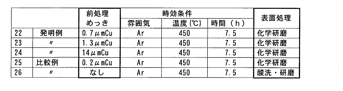
本発明の請求項7に記載の製造方法に関する発明例について説明する。発明例22〜24および比較例25、26のそれぞれについて、表6に示すめっき処理条件、時効処理条件および表面処理条件の下、表7に示す結果を得た。
【0049】
【表6】
【表7】
表6に示すように、発明例22〜24は、最終圧延材にCuめっきを施した後に、時効処理を行ない、最後に表面のCuめっきを化学研磨により除去したものである。このため、表7から明らかなように、良好なばね性およびはんだ濡れ性を実現することができた。したがって各発明例については総合評価において優れた結果が得られた。一方、比較例25は0.2μmのCuめっきを施したもので、Cuめっき層が薄いため母材表面が酸化し、良好なはんだ濡れ性を実現することはできなかった。また、比較例26は現行の製造方法を採用した態様であり、時効焼鈍後に材料表面に機械研磨を施したことから高いばね限界値が得らないため、良好なばね性が実現されなかった。したがって各比較例については総合評価において優れた結果が得られなかった。
【0052】
[本発明の請求項8に記載の製造方法についての検討]
本発明の請求項8に記載の製造方法に関する発明例について説明する。発明例27〜29および比較例30〜32のそれぞれについて表8に示す時効処理条件、表面処理条件および歪取り焼鈍条件の下、表9に示す結果を得た。
【0053】
【表8】
【表9】
表8に示すように、発明例27〜29は、時効焼鈍後化学研磨・機械研磨を施し、次いで歪取り焼鈍を施したものである。表9から明らかなように、発明例27〜29では、機械研磨によって材料の最表層に生じた残留応力を除去することによりばね限界値が回復したため、良好なばね性が実現された。またこれらの発明例27〜29については、化学研磨により材料の表面酸化膜が除去されていることから、良好なはんだ濡れ性を実現することもできた。したがって各発明例については総合評価において優れた結果が得られた。一方、比較例30は、炉内滞留時間が短かいため表面に残留応力が残り、ばね限界値が回復せず優れたばね性を得ることができなかった。また、比較例31は炉内滞留時間が長いため、ばね限界値は耐力レベルにまで回復したものの耐力自体が低下した。さらに、比較例32は現行の製造方法を採用した態様であり、時効焼鈍後に材料表面に機械研磨を施したことから高いばね限界値が得られないため、良好なばね性が実現されなかった。したがって各比較例については総合評価において優れた結果が得られなかった。
【0056】
【発明の効果】
以上説明したように、本発明のCu−Cr−Zr合金によれば、ばね性とはんだ濡れ性とを高いレベルで同時に実現することができる。よって本発明は、近年における軽量化、薄肉化および小型化の要請に十分対応することができる各種電子部品の製造に好適なCu−Cr−Zr合金の製造が可能となる点で極めて有望である。
【図面の簡単な説明】
【図1】残留応力の測定原理を示す図である。
【図2】酸素の検出強度とスパッタリング時間との関係を示すグラフである。
【図3】たわみ試験方法を示す図である。
【図4】(0.2%耐力−ばね限界値)と残留応力との関係を示すグラフである。
【図5】永久変形量と(0.2%耐力−ばね限界値)との関係を示すグラフである。[0001]
TECHNICAL FIELD OF THE INVENTION
The present invention relates to a Cu—Cr—Zr alloy used for manufacturing electronic components such as various terminals, connectors, relays or switches and a method for manufacturing the same, and in particular, achieves high springiness and high solder wettability at the same time. The present invention relates to a technique for producing a Cu—Cr—Zr alloy.
[0002]
[Prior art]
2. Description of the Related Art Inexpensive brass has conventionally been applied to materials that require electrical conductivity and resiliency, such as various terminals, connectors, relays, and switches of electronic devices, for which production cost is important. Phosphor bronze has been used for applications where spring properties are important. Further, nickel silver has been applied to applications where importance is placed on spring properties and corrosion resistance. However, with the recent reduction in the weight, thickness, and size of electronic devices and their components, the required strength cannot be sufficiently satisfied by using these materials. Further, these materials are not always satisfactory in terms of electric conductivity, and from the viewpoint of the performance as a connector, a defect that "the stress relaxation property is poor at the contact portion" has been pointed out.
[0003]
In recent years, materials requiring electrical conductivity and spring properties, such as various terminals, connectors, relays or switches of electronic devices, have been replaced by solid-solution strengthened alloys represented by conventional phosphor bronze, brass, etc., and have high strength and high strength. From the viewpoint of conductivity, the amount of the age hardening type copper alloy is increasing. Age-hardened type copper alloys are prepared by subjecting a solution-treated supersaturated solid solution to aging treatment, whereby fine particles are uniformly precipitated and the strength characteristics such as proof stress and spring limit value are improved, and the amount of solid solution elements is reduced. It contributes to the improvement of the rate.
[0004]
Therefore, an age hardening type copper alloy is used as a material that satisfies increasingly demanding requirements for weight reduction of electronic devices and components thereof and high strength of the materials. Among age-hardened copper alloys, Cu-Cr-Zr-based copper alloys are typical copper alloys having both high strength and high electrical conductivity. Cr and Zr in the Cu—Cr—Zr alloy are active elements, and an active metal may be further added for the purpose of improving the properties of the alloy. In this copper alloy, Cr forms a compound alone, and Zr forms a compound with Cu and precipitates in the base material, whereby strength and conductivity are increased, and a material excellent in bending workability and stress relaxation characteristics is obtained.
[0005]
On the other hand, since a Cu-Cr-Zr alloy contains an active element, a strong oxide film is generated in the aging treatment. For this reason, there is a problem that the solder wettability is significantly reduced. In order to avoid this problem, it is necessary to remove the oxide film by performing chemical polishing (pickling) and mechanical polishing after aging (for example, see Patent Document 1).
[0006]
In the chemical polishing / mechanical polishing step, first, chemical polishing is performed. The oxide film of the Cu—Cr—Zr alloy is very stable to acids. For this reason, it is necessary to use an extremely corrosive chemical polishing liquid such as a solution obtained by mixing hydrogen peroxide with hydrofluoric acid or sulfuric acid for chemical polishing. As described above, by using a chemical polishing liquid having extremely strong corrosive power, not only an oxide film but also an unoxidized portion may be corroded, and unevenness and discoloration may occur on the surface after the chemical polishing. There is. In addition, there is a possibility that the corrosion does not progress uniformly and the oxide film remains locally. Therefore, in order to remove surface irregularities, discoloration, and residual oxide film, after the above chemical polishing, mechanical polishing is performed using, for example, a buff.
[0007]
[Patent Document 1]
JP-A-9-087814
[0008]
[Problems to be solved by the invention]
However, in the Cu—Cr—Zr alloy that has been sequentially subjected to chemical polishing and mechanical polishing, the yield strength (the stress that causes permanent deformation when the sample is pulled) does not change, but the spring limit value (when the sample is bent). However, there is a problem that the stress which causes permanent deformation is reduced. This is because the spring limit value increased by the aging treatment decreases again by the chemical polishing and the mechanical polishing. Therefore, a conventional electronic component uses a Cu—Cr—Zr alloy having a spring limit significantly lower than the proof stress, or a Cu—Cr—Zr alloy having a thick oxide film even if it has a proof stress spring limit. It had been.
[0009]
When spring components such as connectors, relays, and switches are manufactured using materials with low spring limits, permanent deformation (set) is likely to occur in the movable part when inserting or removing the connector. was there. When the sag occurs, the contact pressure at the electrical contact decreases, and the electrical resistance at the contact increases. On the other hand, when a spring component is manufactured using a material having a thick oxide film, the oxide film of the Cu—Cr—Zr alloy is particularly strong, so that the solder wettability deteriorates remarkably. Therefore, the development of a Cu—Cr—Zr alloy that realizes excellent spring properties by having a high spring limit value that does not cause the above set, and that also has excellent solder wettability has been demanded.
[0010]
Therefore, the present invention has been made in view of the above requirements, and an object of the present invention is to provide a Cu-Cr-Zr alloy that simultaneously realizes a high level of springability and solder wettability and a method of manufacturing the same. I have.
[0011]
[Means for Solving the Problems]
The Cu—Cr—Zr alloy of the present invention is a copper-based alloy containing 0.02 to 0.4% of Cr and 0.01 to 0.25% of Zr, with the balance being Cu and unavoidable impurities. , The 0.2% proof stress is 500 MPa or more, the difference between the 0.2% proof stress and the spring limit value is 100 MPa or less, and the oxide film thickness is 10 nm or less. As a result, sufficient strength can be satisfied even under recent demands for weight reduction of electronic devices and components thereof. Further, the Cu—Cr—Zr alloy of the present invention has a 0.2% proof stress of 500 MPa or more, and the difference between the 0.2% proof stress and the spring limit value is 100 MPa or less. For this reason, the spring limit value is remarkably high with respect to the proof strength, as in the case of a Cu-Cr-Zr alloy which has been sufficiently subjected to chemical polishing and mechanical polishing in addition to having sufficient proof strength for use in electronic devices and the like. By having a high spring limit without lowering, excellent spring properties can be realized. Further, the Cu—Cr—Zr alloy of the present invention can realize excellent solder wettability by setting the oxide film thickness to 10 nm or less.
[0012]
Another Cu-Cr-Zr alloy of the present invention contains 0.02-0.4% of Cr and 0.01-0.25% of Zr, with the balance being Cu and an unavoidable impurity. Wherein the absolute value of the residual stress on the surface is 100 MPa or less, and the oxide film thickness is 10 nm or less. As described above, the Cu—Cr—Zr alloy of the present invention can satisfy sufficient strength by containing Cr in an amount of 0.02 to 0.4% and Zr in an amount of 0.01 to 0.25%. By setting the oxide film thickness to 10 nm or less, excellent solder wettability can be realized. By the way, the present inventors have investigated the cause of the lowering of the spring limit value of the Cu—Cr—Zr alloy in the chemical polishing / mechanical polishing process after aging, and found that the material remained on the outermost layer of the material due to mechanical polishing after chemical polishing. It has been found that stress is generated, and the spring limit value is reduced by the action of the residual stress. Based on this finding, in the Cu—Cr—Zr alloy of the present invention, the absolute value of the residual stress on the surface is set to 100 MPa or less. Therefore, according to the present invention, it is possible to realize a spring property suitable for use in electronic devices and the like.
Further, as the Cu—Cr—Zr alloy of the present invention, 0.05 to 1.5% of Zn, or at least one of Ti, Fe, Ni, Sn, In, Mn, P, Mg, and Si in a total amount of 0% is used. 0.05-1.5%. In addition, it is possible to contain any of these cases.
[0013]
The present inventors have found that, as described above, the cause of the decrease in the spring limit value is the occurrence of residual stress due to mechanical polishing after chemical polishing. Next, the present inventors have found from this finding that a state in which residual stress is low after aging can be realized by preventing the formation of an oxide film on the surface of the Cu-Cr-Zr alloy during aging and omitting mechanical polishing. Got. In addition, it has been found that even if the residual stress once increases in the chemical polishing / mechanical polishing step, a state in which the residual stress is low can be realized by performing a process for reducing the residual stress in a subsequent step. Thus, the present inventors have conducted further intensive studies based on the above findings, and as a specific method for producing a Cu-Cr-Zr alloy,
{Circle around (1)} In an atmosphere containing a large amount of hydrogen, an aging treatment is performed by appropriately selecting a dew point (water vapor concentration), a temperature and a holding time to prevent formation of an oxide film on the surface of the Cu—Cr—Zr alloy during aging. Aspects,
(2) a mode in which a temperature and a holding time are appropriately selected in a high vacuum atmosphere to perform aging treatment to prevent formation of an oxide film on the surface of the Cu—Cr—Zr alloy during aging;
{Circle around (3)} After applying Cu plating to the surface of the Cu—Cr—Zr alloy, aging treatment is performed by appropriately selecting the temperature and the holding time, and then the Cu plating layer (including the surface oxide layer of Cu plating) by chemical polishing. Mode of removing,
{Circle around (4)} Aging treatment is performed by appropriately selecting the temperature and the holding time, then the oxide film is removed by a chemical polishing / mechanical polishing step, and then the dew point (water vapor concentration), the temperature and the temperature in an atmosphere containing a large amount of hydrogen. Mode of performing strain relief annealing to remove residual stress after appropriately selecting the holding time
Was found to be effective. Hereinafter, the method for producing a Cu—Cr—Zr alloy of the present invention will be described for each of the above (1) to (4).
[0014]
In the method for producing a Cu—Cr—Zr alloy according to the present invention, cold rolling is performed after solution treatment, the hydrogen concentration is 50 vol% or more, the balance is made of an inert gas, the dew point is −40 ° C. or less, and 350 to 650. The aging treatment is carried out by holding at 10 ° C. for 10 seconds to 15 hours. The present invention embodies the above mode (1). In the method for producing a Cu—Cr—Zr alloy of the present invention, no mechanical polishing is performed. For this reason, unlike a conventional Cu—Cr—Zr alloy that has been sequentially subjected to chemical polishing and mechanical polishing, the spring limit value does not decrease due to the generation of residual stress due to mechanical polishing. By having this, excellent spring properties can be realized. In the method for producing a Cu—Cr—Zr alloy according to the present invention, aging is performed by appropriately selecting a dew point (water vapor concentration), a temperature and a holding time in an atmosphere containing a large amount of hydrogen. Therefore, the formation of an oxide film on the surface of the Cu—Cr—Zr alloy during aging is prevented, and excellent solder wettability can be realized.
[0015]
In another method for producing a Cu—Cr—Zr alloy of the present invention, cold rolling is performed after solution treatment, and a pressure of 10% is applied.-2The aging treatment is performed by maintaining the temperature at 300 Pa or lower at 300 to 650 ° C. for 10 seconds to 15 hours. The present invention embodies the above mode (2). In the method for producing a Cu—Cr—Zr alloy according to the present invention, since mechanical polishing is not performed, excellent spring properties can be realized as described above. In the method for producing a Cu—Cr—Zr alloy according to the present invention, the aging treatment is performed in a high vacuum atmosphere by appropriately selecting the temperature and the holding time. Therefore, the formation of an oxide film on the surface of the Cu—Cr—Zr alloy during aging is prevented, and excellent solder wettability can be realized.
[0016]
Another manufacturing method of the Cu—Cr—Zr alloy of the present invention is to perform cold rolling after solution treatment, apply a Cu plating having a thickness of 0.5 to 10 μm on the surface, and then apply 10 to 300 to 650 ° C. The aging treatment is performed by holding for a period of seconds to 15 hours, and then the Cu plating layer is removed by chemical polishing. The present invention embodies the mode of the above (3). In the method for producing a Cu—Cr—Zr alloy according to the present invention, since mechanical polishing is not performed, excellent spring properties can be realized as described above. In the method for producing a Cu-Cr-Zr alloy of the present invention, after the Cu-Cr-Zr alloy surface is subjected to Cu plating having a thickness that can be easily removed in a later step, the temperature and the holding time are appropriately selected. An aging treatment is performed, and thereafter, the Cu plating layer (including a surface oxide layer of Cu plating) is removed by chemical polishing. Therefore, even if an oxide film is formed on the Cu plating layer in the aging treatment, the oxide film can be surely removed by subsequently removing the Cu plating layer by chemical polishing. As described above, since the oxide film is removed from the surface of the Cu—Cr—Zr alloy after aging, excellent solder wettability can be realized.
[0017]
Another production method of the Cu—Cr—Zr alloy of the present invention is to perform aging by performing cold rolling after solution treatment and holding at 300 to 650 ° C. for 10 seconds to 15 hours. Is removed by chemical polishing and mechanical polishing, and a strain relief annealing is performed by maintaining the hydrogen concentration at 50 vol% or more, the dew point at -40 ° C. or less, and 400 to 650 ° C. for 5 seconds to 2 minutes. It is characterized by: The present invention embodies the above mode (4). In the method for producing a Cu—Cr—Zr alloy according to the present invention, the aging treatment is performed by appropriately selecting the temperature and the holding time, and then the oxide film is removed by performing chemical polishing and mechanical polishing. This mechanical polishing produces residual stress in the outermost layer of the material, and the action of the residual stress lowers the spring limit. Therefore, strain relief annealing for removing residual stress is performed after mechanical polishing. As described above, even if the residual stress once increases in the chemical polishing / mechanical polishing process, a state in which the residual stress is low can be realized by performing a process of reducing the residual stress in a subsequent process. Therefore, by having a high spring limit value, excellent spring properties can be realized. Further, by performing the strain relief annealing in an atmosphere containing a large amount of hydrogen by appropriately selecting the dew point (water vapor concentration), the temperature, and the holding time, the Cu—Cr—Zr alloy surface during the strain relief annealing is performed. Oxidation can be suppressed, and excellent solder wettability can be obtained.
[0018]
Next, the reasons for limiting the component composition and the production conditions of the present invention will be specifically described.
Cr
Cr has a function of improving strength and heat resistance by precipitating in the base material upon aging treatment, but if the content is less than 0.02%, a desired effect due to the above-mentioned effect cannot be expected. On the other hand, if the content of Cr exceeds 0.4%, undissolved Cr remains in the base material even after the solution treatment and the conductivity and workability are remarkably reduced. 0.02 to 0.4%.
Zr
Zr has a function of forming a compound with Cu by aging treatment and precipitating in the base material to strengthen it, but if its content is less than 0.01%, the desired effect due to the above-mentioned effect cannot be obtained. On the other hand, if Zr is contained in excess of 0.25%, undissolved Zr will remain in the base material even after the solution treatment, causing a significant decrease in conductivity and workability. Was set to 0.01 to 0.25%.
[0019]
Zn concentration
Zn is a component that is added as necessary because it has an effect of improving the heat-peeling resistance of solder. However, if its content is less than 0.05%, the desired effect due to the above-mentioned effect cannot be obtained. If the Zn content exceeds 0.3%, the electrical conductivity and the stress relaxation characteristics deteriorate, so the Zn content is determined to be 0.05 to 0.3%.
Ti, Fe, Ni, Sn, In, Mn, P, Mg and Si
Ti, Fe, Ni, Sn, In, Mn, P, Mg and Si have an effect of improving the strength and conductivity of the Cu-Cr-Zr alloy. In addition, among these, Ti forms an intermetallic compound with Ni in the base material, and Fe forms an intermetallic compound with Ti in the base material. There is. Sn, In, Mn, P, Mg and Si all have the effect of improving the strength by solid solution strengthening without significantly lowering the conductivity of the alloy. If the total content of Ti, Fe, Ni, Sn, In, Mn, P, Mg and Si is less than 0.05%, the above effects cannot be obtained, and if the total content exceeds 1.5%. The conductivity is significantly reduced. Therefore, their contents are determined to be 0.05 to 1.5% in total.
Oxide film thickness
If the oxide film thickness exceeds 10 nm, the solder wettability decreases. Therefore, the oxide film thickness is limited to 10 nm or less.
[0020]
0.2% proof stress
The 0.2% proof stress needs to be 500 MPa or more in the design of the connector. In addition, in order to obtain sufficient spring strength, 550 MPa or more is desirable.
Spring limit value
In order to obtain a spring characteristic corresponding to the 0.2% proof stress of the alloy, it is necessary to set the spring limit value to (0.2% proof stress-100) MPa or more. Since the connector is designed based on the proof stress of the material, if the spring limit value is lower than (0.2% proof stress-100) MPa, the above-mentioned sag occurs, and a desired contact pressure cannot be obtained.
[0021]
Residual stress
In order to obtain a spring limit value of (0.2% proof stress-100) MPa or more, the absolute value of the residual stress on the surface needs to be 100 MPa or less.
[0022]
Solution treatment
The solution treatment conditions are not particularly limited, but the solution treatment is performed in order to obtain a high-strength material by the subsequent aging treatment. The higher the treatment temperature, the greater the amount of Cr and Zr dissolved in the matrix and the higher the strength after aging. In order to obtain such an effect, the higher the processing temperature, the better, and it is preferable to set the processing temperature to 700 ° C. or higher. In the solution treatment, a higher cooling rate facilitates obtaining high strength. Specifically, it is desirable to perform water cooling.
[0023]
Cold rolling
The reason for performing cold rolling after the solution treatment is to further accelerate the precipitation rate of precipitates in the work hardening and aging steps in order to increase the strength. The degree of work in cold rolling is not particularly limited, but if the degree of work in cold rolling is less than 50%, the above effect is insufficient, and if the degree of work exceeds 90%, bending workability deteriorates. The working ratio (R) is defined by the following equation.
R = (t0−t) / t0(T0: Thickness before rolling, t: thickness after rolling)
[0024]
Aging temperature and aging time
In order to improve strength and conductivity, it is important to perform aging treatment for 10 seconds to 15 hours in a temperature range of 300 to 650 ° C. The aging temperature is the atmospheric temperature inside the heating furnace, and the aging time is the time during which the material stays in the heating furnace. Since the solid solution amounts of Cr and Zr in Cu decrease as the temperature decreases, the amount of precipitation increases with aging at a low temperature, and higher strength and conductivity can be obtained. However, since the time required for the aging treatment becomes longer, the manufacturing cost becomes higher. On the other hand, the higher the temperature, the higher the precipitation rate of the fine particles. Therefore, as the aging is performed at a higher temperature, the predetermined conductivity and strength can be obtained in a shorter time. However, the ultimate values of the conductivity and the strength may be low. Therefore, it is desirable to appropriately select the aging temperature and the aging time depending on the manufacturing cost and the target characteristics.
[0025]
If the aging temperature is lower than 300 ° C., the aging treatment takes an extremely long time, which is not preferable from the viewpoint of manufacturing economy. On the other hand, when the aging temperature exceeds 650 ° C., the amount of precipitation decreases, and strength and conductivity are hardly improved. If the aging time is less than 10 seconds, a sufficient amount of precipitation cannot be obtained, and strength and conductivity are not improved. On the other hand, if the aging time exceeds 15 hours, not only is the production cost relatively high, but if a relatively high aging temperature is selected, the precipitates become coarse and the strength is lowered, which is not preferable.
[0026]
Means for suppressing formation of oxide film
Means for reducing the oxide film thickness to 10 nm or less will be described in detail by classifying them into the following cases (1) to (4).
(1) Aging treatment is performed in an inert gas mixed with hydrogen. In order to control the oxide film thickness to 10 nm or less, it is necessary to set the hydrogen concentration to 50 vol% or more and to set the dew point to -40 ° C. or less. Nitrogen or argon can be used as the inert gas. The pressure of the gas is not limited, but usually a pressure slightly higher than the atmospheric pressure is employed.
[0027]
(2) Aging is performed in a high vacuum atmosphere. In order to control the oxide film thickness to 10 nm or less, the pressure must be 10-2It is necessary to make it Pa or less.
[0028]
(3) Cu plating is applied to the material surface before aging. Cu is less likely to be oxidized than a Cu—Cr—Zr alloy, and its oxide film can be easily removed by chemical polishing together with the plated Cu itself. After Cu plating, aging treatment is performed in a conventional atmosphere such as an inert gas, and finally, an oxide film formed on the Cu plating by chemical polishing is dissolved and removed together with the Cu plating layer. Cu plating can be performed under general manufacturing conditions using a bath such as copper sulfate. However, it is necessary to control the plating thickness to 0.5 to 10 μm. If the plating thickness is less than 0.5 μm, an oxide film may be formed on the Cu—Cr—Zr alloy as the base material. If chemical polishing is performed until the oxide film is removed, irregularities and discoloration are likely to occur on the surface, and mechanical polishing cannot be omitted. On the other hand, when the thickness of the Cu plating exceeds 10 μm, not only is the production cost relatively high, but also it is difficult to remove the Cu plating layer by chemical polishing. As the chemical polishing liquid, for example, a solution in which a small amount of hydrogen peroxide is mixed with sulfuric acid can be used.
[0029]
(4) After performing aging treatment in a conventional atmosphere such as an inert gas, an oxide film formed by aging is removed by chemical polishing or mechanical polishing. Among these polishing steps, residual stress is generated in the outermost layer of the material in the mechanical polishing step, and the action of the residual stress lowers the spring limit value. However, in the next step, strain relief annealing is performed to remove residual stress and improve the spring limit value. The strain relief annealing employs continuous annealing, and is performed at a temperature of 400 to 650 ° C. for 5 seconds to 2 minutes. When the temperature is lower than 400 ° C., the residual stress is not removed, and when the temperature is higher than 650 ° C., the precipitate re-dissolves, and the strength and the electrical conductivity are significantly reduced. If the time is less than 5 seconds, the residual stress is not removed, and if it exceeds 2 minutes, the 0.2% proof stress is significantly reduced. In order to control the oxide film thickness generated by the strain relief annealing to 10 nm or less, it is necessary to set the hydrogen concentration to 50 vol% or more and to set the dew point to -40 ° C. or less. Nitrogen or argon can be used as the inert gas. The pressure of the gas is not limited, but usually a pressure slightly higher than the atmospheric pressure can be employed.
[0030]
[Example of the invention]
Next, examples of the present invention will be described.
An ingot having a thickness of 30 mm was cast using a high-frequency vacuum melting furnace using electrolytic copper or oxygen-free copper as a main raw material, a copper chromium master alloy, a copper zirconium master alloy, and zinc as auxiliary raw materials. This ingot was formed into a plate having a thickness of 0.15 mm in accordance with the above-mentioned steps, subjected to aging treatment under various conditions, and evaluated for residual stress, oxide film thickness, solder wettability, and spring limit value (spring property). Furthermore, a comprehensive evaluation was performed to determine whether both the spring limit value and the solder wettability exhibited excellent results. Each evaluation method is shown below.
[0031]
Residual stress
The residual stress generated in the direction parallel to the rolling direction with respect to the (113) plane was determined by the X-ray diffraction method. The principle and calculation formula of the stress measurement are shown below.
・ Principle of measuring residual stress
As shown in FIG. 1, when the angle ψ formed between the sample surface normal N and the lattice surface normal N ′ is changed and the change in the diffraction angle (2θ) is investigated, the residual stress σ can be obtained by the following equation. .
[0032]
(Equation 1)
In the above equation, K (stress constant) is a constant determined by the material and the diffraction angle. 2θ / sin from measured value2Draw a diagram of ψ, then find the gradient by the least squares method and multiply by K to get the residual stress.
Oxide film thickness
The oxide film thickness was measured by Auger electron spectroscopy. The measurement of the oxygen intensity and the Ar sputtering of the surface were alternately performed to obtain a graph shown in FIG. In the figure, the sputtering time when the detected intensity of oxygen becomes an intermediate value between the maximum value at the surface and the value at the non-oxidized portion was determined, and this time was regarded as the time required for sputtering the oxide film. The oxide film thickness becomes SiO2Obtained by multiplying the sputtering rate of the coating.
[0034]
Solder wettability
According to JIS-0053 (1996), the time at which wetting started was measured by the meniscograph method. The measurement conditions are as follows. The sample was degreased using acetone as a pretreatment. Next, chemical polishing was performed using a 10 vol% sulfuric acid aqueous solution. The solder used was 60% Pb-40% Sn, and the measurement temperature was 235 ° C. As flux, GX5 manufactured by Asahi Chemical Laboratory Co., Ltd. was used. The immersion depth was 2 mm, the immersion time was 10 seconds, the immersion speed was 15 mm / sec, and the width of the sample was 10 mm. The evaluation criterion was that a sample having a time of 1 second or less until the start of wetting was evaluated as good (○), and a sample longer than 1 second was evaluated as poor (×).
[0035]
0.2% proof stress and spring limit value
The proof stress in a direction parallel to the rolling direction was measured by a tensile tester. Further, a spring limit value in a direction parallel to the rolling direction was measured by a moment type test specified in JIS-H3130. The evaluation criteria for the spring property were those in which the spring limit value was (proof stress −100 (MPa)) or more was evaluated as good (○), and those with less than (proof stress −100 (MPa)) were evaluated as poor (×).
Deflection test
In order to evaluate the performance as an electronic component material, as shown in FIG. 3, one end of the test piece was fixed, and a load f was applied to a position at a distance 1 from the fixed end to give a deflection f. After removing the load, the amount of permanent deformation δ of the sample was measured. The width W of the sample was 10 mm, and the sample was prepared such that the longitudinal direction of the sample was parallel to the rolling direction. Also, l = 10 mm and f = 5 mm. The stress generated on the sample surface at this time is expressed by the cantilever beam equation
σ = 6P · l / (W · t2) (T: sample thickness)
It was about 450 MPa when calculated using.
[0036]
Hereinafter, matters actually examined by the applicant will be described.
[Consideration of conventional manufacturing method]
After performing an aging treatment at 450 ° C. for 7.5 hours in an Ar gas atmosphere at a dew point of −10 ° C., the surface was subjected to mechanical polishing. In this polishing, the polishing amount was variously changed. After polishing, the 0.2% proof stress, the spring limit value, the residual stress on the surface, the oxide film thickness and the solder wettability were measured. In addition, the amount of permanent deformation when a predetermined deflection was given to the sample by the method of FIG. 3 was measured. Table 1 shows the results.
[0037]
[Table 1]
In the table, the larger the number of the sample, the larger the mechanical polishing amount. It can be seen that the more mechanical polishing is performed, the greater the compressive residual stress generated on the sample surface. As shown in FIG. 4, when the residual stress increases, the spring limit value decreases, and the spring property gradually deteriorates. When the residual stress exceeds 100 MPa, the difference between the 0.2% proof stress and the spring limit value exceeds 100 MPa. In addition, as shown in FIG. 5, when the difference between the 0.2% proof stress and the spring limit value exceeds 100 MPa, permanent deformation occurs when a predetermined deflection is given to the sample. The amount of permanent deformation increases as the difference between the 0.2% proof stress and the spring limit value increases. Such permanent deformation is not preferable because it causes a decrease in contact pressure at the connector contact.
[0039]
On the other hand, as the amount of mechanical polishing increases, the oxide film thickness decreases, and when the oxide film thickness is 10 nm or less, good solder wettability is realized. Sex was not realized. From the above, in Conventional Examples 1 to 9 shown in Table 1, the spring limit value and the solder wettability were not compatible at a high level, and excellent results were not obtained in the comprehensive evaluation.
[0040]
[Study on the manufacturing method according to claim 5 of the present invention]
An example of the invention relating to the manufacturing method according to claim 5 of the present invention will be described. The results shown in Table 3 were obtained under the aging treatment conditions shown in Table 2 for each of Invention Examples 10 to 12 and Comparative Examples 13 to 15. In addition, about each invention example and each comparative example, surface treatments, such as chemical polishing and mechanical polishing, are not given after aging.
[0041]
[Table 2]
[Table 3]
As shown in Table 2, for Invention Examples 10 to 12, the aging treatment was performed by setting the dew point in the annealing furnace to −40 ° C. or less. As is clear from Table 3, with respect to Inventive Examples 10 to 12, the surface did not oxidize, achieved good solder wettability, and had good spring properties. Therefore, excellent results were obtained in the overall evaluation for each invention example. On the other hand, in Comparative Examples 13 to 15, the aging treatment was performed with the dew point in the annealing furnace higher than -40C. In Comparative Examples 13 to 15, although the high spring limit was obtained, the spring property was good, but the surface was oxidized, so that good solder wettability was not obtained. Therefore, excellent results were not obtained in the overall evaluation for each comparative example.
[0044]
[Study on the manufacturing method according to claim 6 of the present invention]
An example of the invention relating to the manufacturing method according to claim 6 of the present invention will be described. The results shown in Table 5 were obtained under the aging treatment conditions shown in Table 4 for each of Invention Examples 16 to 18 and Comparative Examples 19 to 21. In addition, about each invention example and each comparative example, surface treatments, such as chemical polishing and mechanical polishing, are not performed after aging.
[0045]
[Table 4]
[Table 5]
As shown in Table 4, Invention Examples 16 to 18 had a vacuum degree of 10 in the annealing furnace.-2The aging treatment was performed at a Pa or lower. As is clear from Table 5, Invention Example 16 achieved good solder wettability together with Invention Examples 17 and 18, although the surface oxidation was slightly caused, and also showed good spring properties. Therefore, excellent results were obtained in the overall evaluation for each invention example. On the other hand, in Comparative Examples 19 to 21, the degree of vacuum in the annealing furnace was 10-2The aging annealing was performed at a pressure higher than Pa. In Comparative Examples 19 to 21, although the spring property was good, the surface was oxidized, so that good solder wettability could not be realized. Therefore, excellent results were not obtained in the overall evaluation for each comparative example.
[0048]
[Study on the manufacturing method according to claim 7 of the present invention]
An example of the invention relating to the manufacturing method according to claim 7 of the present invention will be described. For each of Invention Examples 22 to 24 and Comparative Examples 25 and 26, the results shown in Table 7 were obtained under the plating treatment conditions, aging treatment conditions, and surface treatment conditions shown in Table 6.
[0049]
[Table 6]
[Table 7]
As shown in Table 6, in Inventive Examples 22 to 24, the aging treatment was performed after Cu plating was applied to the final rolled material, and finally the Cu plating on the surface was removed by chemical polishing. Therefore, as is clear from Table 7, good spring properties and solder wettability could be realized. Therefore, excellent results were obtained in the overall evaluation for each invention example. On the other hand, in Comparative Example 25, the Cu plating of 0.2 μm was applied, and the surface of the base material was oxidized because the Cu plating layer was thin, so that good solder wettability could not be realized. In Comparative Example 26, the current production method was adopted. Since the material surface was subjected to mechanical polishing after the aging annealing, a high spring limit value was not obtained, so that good spring properties were not realized. Therefore, excellent results were not obtained in the overall evaluation for each comparative example.
[0052]
[Study on the manufacturing method according to claim 8 of the present invention]
An example of the invention relating to the manufacturing method according to claim 8 of the present invention will be described. The results shown in Table 9 were obtained for each of Inventive Examples 27 to 29 and Comparative Examples 30 to 32 under the aging treatment conditions, surface treatment conditions, and strain relief annealing conditions shown in Table 8.
[0053]
[Table 8]
[Table 9]
As shown in Table 8, Inventive Examples 27 to 29 were subjected to chemical polishing and mechanical polishing after aging annealing, and then to strain relief annealing. As is clear from Table 9, in Examples 27 to 29, the spring limit was restored by removing the residual stress generated in the outermost layer of the material by the mechanical polishing, so that good spring properties were realized. In these Inventive Examples 27 to 29, since the surface oxide film of the material was removed by the chemical polishing, good solder wettability was able to be realized. Therefore, excellent results were obtained in the overall evaluation for each invention example. On the other hand, in Comparative Example 30, since the residence time in the furnace was short, residual stress remained on the surface, and the spring limit value was not recovered, and excellent spring properties could not be obtained. In Comparative Example 31, since the residence time in the furnace was long, the spring limit value was restored to the proof stress level, but the proof stress itself was reduced. Further, Comparative Example 32 is an aspect in which the current production method was adopted, and a high spring limit value was not obtained because the material surface was subjected to mechanical polishing after the aging annealing, so that good spring properties were not realized. Therefore, excellent results were not obtained in the overall evaluation for each comparative example.
[0056]
【The invention's effect】
As described above, according to the Cu—Cr—Zr alloy of the present invention, the spring property and the solder wettability can be simultaneously realized at a high level. Therefore, the present invention is extremely promising in that it enables production of a Cu—Cr—Zr alloy suitable for production of various electronic components that can sufficiently respond to recent demands for weight reduction, thinning, and miniaturization. .
[Brief description of the drawings]
FIG. 1 is a view showing a principle of measuring a residual stress.
FIG. 2 is a graph showing a relationship between a detected intensity of oxygen and a sputtering time.
FIG. 3 is a diagram showing a deflection test method.
FIG. 4 is a graph showing a relationship between (0.2% proof stress-spring limit value) and residual stress.
FIG. 5 is a graph showing the relationship between the amount of permanent deformation and (0.2% proof stress-spring limit value).
Claims (8)
Priority Applications (1)
| Application Number | Priority Date | Filing Date | Title |
|---|---|---|---|
| JP2003051833A JP2004256902A (en) | 2003-02-27 | 2003-02-27 | Cu-Cr-Zr ALLOY, AND PRODUCTION METHOD THEREFOR |
Applications Claiming Priority (1)
| Application Number | Priority Date | Filing Date | Title |
|---|---|---|---|
| JP2003051833A JP2004256902A (en) | 2003-02-27 | 2003-02-27 | Cu-Cr-Zr ALLOY, AND PRODUCTION METHOD THEREFOR |
Publications (1)
| Publication Number | Publication Date |
|---|---|
| JP2004256902A true JP2004256902A (en) | 2004-09-16 |
Family
ID=33116881
Family Applications (1)
| Application Number | Title | Priority Date | Filing Date |
|---|---|---|---|
| JP2003051833A Pending JP2004256902A (en) | 2003-02-27 | 2003-02-27 | Cu-Cr-Zr ALLOY, AND PRODUCTION METHOD THEREFOR |
Country Status (1)
| Country | Link |
|---|---|
| JP (1) | JP2004256902A (en) |
Cited By (11)
| Publication number | Priority date | Publication date | Assignee | Title |
|---|---|---|---|---|
| JP2010126783A (en) * | 2008-11-28 | 2010-06-10 | Nippon Mining & Metals Co Ltd | Copper alloy sheet or strip for electronic material |
| JP2014077192A (en) * | 2012-09-20 | 2014-05-01 | Jx Nippon Mining & Metals Corp | Copper alloy and connector terminal material for high current |
| WO2014064961A1 (en) * | 2012-10-22 | 2014-05-01 | Jx日鉱日石金属株式会社 | Copper alloy plate exhibiting excellent conductivity and stress-relaxation properties |
| JP2014101580A (en) * | 2012-10-22 | 2014-06-05 | Jx Nippon Mining & Metals Corp | Copper alloy sheet having excellent conductivity and stress relaxation characteristics |
| JP2014198894A (en) * | 2013-03-14 | 2014-10-23 | Jx日鉱日石金属株式会社 | Copper alloy sheet excellent in conductivity and stress relief property |
| JP2015101773A (en) * | 2013-11-26 | 2015-06-04 | Jx日鉱日石金属株式会社 | Copper alloy sheet excellent in conductivity and stress relaxation property |
| CN112080663A (en) * | 2020-08-28 | 2020-12-15 | 陕西斯瑞新材料股份有限公司 | Method for manufacturing electrode rod made of chromium-zirconium-copper alloy material |
| CN114752808A (en) * | 2022-04-19 | 2022-07-15 | 有研工程技术研究院有限公司 | High-strength high-conductivity copper alloy composite material and preparation method thereof |
| CN115647741A (en) * | 2022-10-31 | 2023-01-31 | 无锡晨锌钢结构有限公司 | Production process of solar photovoltaic bracket |
| CN116219335A (en) * | 2023-02-28 | 2023-06-06 | 洛阳船舶材料研究所(中国船舶集团有限公司第七二五研究所) | A Method of Improving the Corrosion Fatigue Strength of Marine Copper Alloy |
| CN121496226A (en) * | 2026-01-13 | 2026-02-10 | 河南科技大学 | A high-strength, high-conductivity Cu-Zr-Cr alloy and its preparation method |
-
2003
- 2003-02-27 JP JP2003051833A patent/JP2004256902A/en active Pending
Cited By (14)
| Publication number | Priority date | Publication date | Assignee | Title |
|---|---|---|---|---|
| JP2010126783A (en) * | 2008-11-28 | 2010-06-10 | Nippon Mining & Metals Co Ltd | Copper alloy sheet or strip for electronic material |
| JP2014077192A (en) * | 2012-09-20 | 2014-05-01 | Jx Nippon Mining & Metals Corp | Copper alloy and connector terminal material for high current |
| CN104718302A (en) * | 2012-10-22 | 2015-06-17 | Jx日矿日石金属株式会社 | Copper alloy plate exhibiting excellent conductivity and stress-relaxation properties |
| WO2014064961A1 (en) * | 2012-10-22 | 2014-05-01 | Jx日鉱日石金属株式会社 | Copper alloy plate exhibiting excellent conductivity and stress-relaxation properties |
| JP2014101574A (en) * | 2012-10-22 | 2014-06-05 | Jx Nippon Mining & Metals Corp | Copper alloy sheet having excellent conductivity and stress relaxation characteristics |
| JP2014101580A (en) * | 2012-10-22 | 2014-06-05 | Jx Nippon Mining & Metals Corp | Copper alloy sheet having excellent conductivity and stress relaxation characteristics |
| JP2014133949A (en) * | 2012-10-22 | 2014-07-24 | Jx Nippon Mining & Metals Corp | Copper alloy sheet excellent in conductivity and stress relaxation property |
| JP2014198894A (en) * | 2013-03-14 | 2014-10-23 | Jx日鉱日石金属株式会社 | Copper alloy sheet excellent in conductivity and stress relief property |
| JP2015101773A (en) * | 2013-11-26 | 2015-06-04 | Jx日鉱日石金属株式会社 | Copper alloy sheet excellent in conductivity and stress relaxation property |
| CN112080663A (en) * | 2020-08-28 | 2020-12-15 | 陕西斯瑞新材料股份有限公司 | Method for manufacturing electrode rod made of chromium-zirconium-copper alloy material |
| CN114752808A (en) * | 2022-04-19 | 2022-07-15 | 有研工程技术研究院有限公司 | High-strength high-conductivity copper alloy composite material and preparation method thereof |
| CN115647741A (en) * | 2022-10-31 | 2023-01-31 | 无锡晨锌钢结构有限公司 | Production process of solar photovoltaic bracket |
| CN116219335A (en) * | 2023-02-28 | 2023-06-06 | 洛阳船舶材料研究所(中国船舶集团有限公司第七二五研究所) | A Method of Improving the Corrosion Fatigue Strength of Marine Copper Alloy |
| CN121496226A (en) * | 2026-01-13 | 2026-02-10 | 河南科技大学 | A high-strength, high-conductivity Cu-Zr-Cr alloy and its preparation method |
Similar Documents
| Publication | Publication Date | Title |
|---|---|---|
| CN101512026B (en) | Cu-ni-si alloy | |
| JP4809602B2 (en) | Copper alloy | |
| JPWO2010013790A1 (en) | Copper alloy material for electric and electronic parts and manufacturing method thereof | |
| WO2011118400A1 (en) | High-strength copper titanium plate and production method therefor | |
| WO2006106939A1 (en) | Cu-Ni-Si-Co-Cr BASED COPPER ALLOY FOR ELECTRONIC MATERIAL AND METHOD FOR PRODUCTION THEREOF | |
| JP5619389B2 (en) | Copper alloy material | |
| JP5417366B2 (en) | Cu-Ni-Si alloy with excellent bending workability | |
| KR101338710B1 (en) | Ni-si-co copper alloy and manufacturing method therefor | |
| JP4386236B2 (en) | Cu-Ni-Si alloy | |
| JPWO2010016428A1 (en) | Copper alloy material for electrical and electronic parts | |
| WO2018079507A1 (en) | Copper alloy sheet and method for manufacturing same | |
| WO2012132765A1 (en) | Cu-si-co-base copper alloy for electronic materials and method for producing same | |
| JP5539932B2 (en) | Cu-Co-Si alloy with excellent bending workability | |
| WO2011019042A1 (en) | Copper alloy material for electrical/electronic components | |
| WO2009116649A1 (en) | Copper alloy material for electric and electronic components | |
| JP2004256902A (en) | Cu-Cr-Zr ALLOY, AND PRODUCTION METHOD THEREFOR | |
| JP6835638B2 (en) | Copper alloy plate with excellent strength and conductivity | |
| CN106460097B (en) | The manufacture method of copper alloy plate and copper alloy plate | |
| WO2011039875A1 (en) | Tin-plated cu-ni-si-based alloy strip having excellent resistance to heat separation of the tin-plating | |
| JP6077755B2 (en) | Cu-Zn-Sn-Ni-P-based alloy and manufacturing method thereof | |
| JP4068413B2 (en) | Cu-Ti alloy and method for producing the same | |
| JP4708833B2 (en) | High strength copper alloy material for precision conductive spring with excellent sag resistance and its manufacturing method | |
| JP2012229467A (en) | Cu-Ni-Si BASED COPPER ALLOY FOR ELECTRONIC MATERIAL | |
| JP4820228B2 (en) | Cu-Zn-Sn alloy strips with excellent heat-resistant peelability for Sn plating and Sn plating strips thereof | |
| JP4175920B2 (en) | High strength copper alloy |
Legal Events
| Date | Code | Title | Description |
|---|---|---|---|
| A621 | Written request for application examination |
Free format text: JAPANESE INTERMEDIATE CODE: A621 Effective date: 20050916 |
|
| A711 | Notification of change in applicant |
Effective date: 20060427 Free format text: JAPANESE INTERMEDIATE CODE: A712 |
|
| A977 | Report on retrieval |
Free format text: JAPANESE INTERMEDIATE CODE: A971007 Effective date: 20070606 |
|
| A131 | Notification of reasons for refusal |
Effective date: 20070626 Free format text: JAPANESE INTERMEDIATE CODE: A131 |
|
| A521 | Written amendment |
Free format text: JAPANESE INTERMEDIATE CODE: A523 Effective date: 20070824 |
|
| A131 | Notification of reasons for refusal |
Free format text: JAPANESE INTERMEDIATE CODE: A131 Effective date: 20081021 |
|
| A02 | Decision of refusal |
Free format text: JAPANESE INTERMEDIATE CODE: A02 Effective date: 20090310 |