JP2004260165A - Cmosに適用する複数の金属ゲートを集積するシステムおよび方法 - Google Patents
Cmosに適用する複数の金属ゲートを集積するシステムおよび方法 Download PDFInfo
- Publication number
- JP2004260165A JP2004260165A JP2004039093A JP2004039093A JP2004260165A JP 2004260165 A JP2004260165 A JP 2004260165A JP 2004039093 A JP2004039093 A JP 2004039093A JP 2004039093 A JP2004039093 A JP 2004039093A JP 2004260165 A JP2004260165 A JP 2004260165A
- Authority
- JP
- Japan
- Prior art keywords
- metal layer
- thickness
- work function
- gate
- overlying
- Prior art date
- Legal status (The legal status is an assumption and is not a legal conclusion. Google has not performed a legal analysis and makes no representation as to the accuracy of the status listed.)
- Pending
Links
Images




Classifications
-
- H—ELECTRICITY
- H10—SEMICONDUCTOR DEVICES; ELECTRIC SOLID-STATE DEVICES NOT OTHERWISE PROVIDED FOR
- H10D—INORGANIC ELECTRIC SEMICONDUCTOR DEVICES
- H10D30/00—Field-effect transistors [FET]
- H10D30/01—Manufacture or treatment
- H10D30/021—Manufacture or treatment of FETs having insulated gates [IGFET]
- H10D30/0223—Manufacture or treatment of FETs having insulated gates [IGFET] having source and drain regions or source and drain extensions self-aligned to sides of the gate
- H10D30/0225—Manufacture or treatment of FETs having insulated gates [IGFET] having source and drain regions or source and drain extensions self-aligned to sides of the gate using an initial gate mask complementary to the prospective gate location, e.g. using dummy source and drain electrodes
-
- H—ELECTRICITY
- H10—SEMICONDUCTOR DEVICES; ELECTRIC SOLID-STATE DEVICES NOT OTHERWISE PROVIDED FOR
- H10D—INORGANIC ELECTRIC SEMICONDUCTOR DEVICES
- H10D30/00—Field-effect transistors [FET]
- H10D30/60—Insulated-gate field-effect transistors [IGFET]
-
- H—ELECTRICITY
- H10—SEMICONDUCTOR DEVICES; ELECTRIC SOLID-STATE DEVICES NOT OTHERWISE PROVIDED FOR
- H10D—INORGANIC ELECTRIC SEMICONDUCTOR DEVICES
- H10D64/00—Electrodes of devices having potential barriers
- H10D64/60—Electrodes characterised by their materials
- H10D64/66—Electrodes having a conductor capacitively coupled to a semiconductor by an insulator, e.g. MIS electrodes
- H10D64/665—Electrodes having a conductor capacitively coupled to a semiconductor by an insulator, e.g. MIS electrodes the conductor comprising a layer of elemental metal contacting the insulator, e.g. tungsten or molybdenum
-
- H—ELECTRICITY
- H10—SEMICONDUCTOR DEVICES; ELECTRIC SOLID-STATE DEVICES NOT OTHERWISE PROVIDED FOR
- H10D—INORGANIC ELECTRIC SEMICONDUCTOR DEVICES
- H10D64/00—Electrodes of devices having potential barriers
- H10D64/60—Electrodes characterised by their materials
- H10D64/66—Electrodes having a conductor capacitively coupled to a semiconductor by an insulator, e.g. MIS electrodes
- H10D64/665—Electrodes having a conductor capacitively coupled to a semiconductor by an insulator, e.g. MIS electrodes the conductor comprising a layer of elemental metal contacting the insulator, e.g. tungsten or molybdenum
- H10D64/666—Electrodes having a conductor capacitively coupled to a semiconductor by an insulator, e.g. MIS electrodes the conductor comprising a layer of elemental metal contacting the insulator, e.g. tungsten or molybdenum the conductor further comprising additional layers
-
- H—ELECTRICITY
- H10—SEMICONDUCTOR DEVICES; ELECTRIC SOLID-STATE DEVICES NOT OTHERWISE PROVIDED FOR
- H10D—INORGANIC ELECTRIC SEMICONDUCTOR DEVICES
- H10D64/00—Electrodes of devices having potential barriers
- H10D64/60—Electrodes characterised by their materials
- H10D64/66—Electrodes having a conductor capacitively coupled to a semiconductor by an insulator, e.g. MIS electrodes
- H10D64/667—Electrodes having a conductor capacitively coupled to a semiconductor by an insulator, e.g. MIS electrodes the conductor comprising a layer of alloy material, compound material or organic material contacting the insulator, e.g. TiN workfunction layers
-
- H—ELECTRICITY
- H10—SEMICONDUCTOR DEVICES; ELECTRIC SOLID-STATE DEVICES NOT OTHERWISE PROVIDED FOR
- H10D—INORGANIC ELECTRIC SEMICONDUCTOR DEVICES
- H10D84/00—Integrated devices formed in or on semiconductor substrates that comprise only semiconducting layers, e.g. on Si wafers or on GaAs-on-Si wafers
- H10D84/01—Manufacture or treatment
- H10D84/0123—Integrating together multiple components covered by H10D12/00 or H10D30/00, e.g. integrating multiple IGBTs
- H10D84/0126—Integrating together multiple components covered by H10D12/00 or H10D30/00, e.g. integrating multiple IGBTs the components including insulated gates, e.g. IGFETs
- H10D84/0165—Integrating together multiple components covered by H10D12/00 or H10D30/00, e.g. integrating multiple IGBTs the components including insulated gates, e.g. IGFETs the components including complementary IGFETs, e.g. CMOS devices
- H10D84/0172—Manufacturing their gate conductors
- H10D84/0177—Manufacturing their gate conductors the gate conductors having different materials or different implants
-
- H—ELECTRICITY
- H10—SEMICONDUCTOR DEVICES; ELECTRIC SOLID-STATE DEVICES NOT OTHERWISE PROVIDED FOR
- H10D—INORGANIC ELECTRIC SEMICONDUCTOR DEVICES
- H10D84/00—Integrated devices formed in or on semiconductor substrates that comprise only semiconducting layers, e.g. on Si wafers or on GaAs-on-Si wafers
- H10D84/01—Manufacture or treatment
- H10D84/02—Manufacture or treatment characterised by using material-based technologies
- H10D84/03—Manufacture or treatment characterised by using material-based technologies using Group IV technology, e.g. silicon technology or silicon-carbide [SiC] technology
- H10D84/038—Manufacture or treatment characterised by using material-based technologies using Group IV technology, e.g. silicon technology or silicon-carbide [SiC] technology using silicon technology, e.g. SiGe
-
- H—ELECTRICITY
- H10—SEMICONDUCTOR DEVICES; ELECTRIC SOLID-STATE DEVICES NOT OTHERWISE PROVIDED FOR
- H10D—INORGANIC ELECTRIC SEMICONDUCTOR DEVICES
- H10D84/00—Integrated devices formed in or on semiconductor substrates that comprise only semiconducting layers, e.g. on Si wafers or on GaAs-on-Si wafers
- H10D84/80—Integrated devices formed in or on semiconductor substrates that comprise only semiconducting layers, e.g. on Si wafers or on GaAs-on-Si wafers characterised by the integration of at least one component covered by groups H10D12/00 or H10D30/00, e.g. integration of IGFETs
- H10D84/82—Integrated devices formed in or on semiconductor substrates that comprise only semiconducting layers, e.g. on Si wafers or on GaAs-on-Si wafers characterised by the integration of at least one component covered by groups H10D12/00 or H10D30/00, e.g. integration of IGFETs of only field-effect components
- H10D84/83—Integrated devices formed in or on semiconductor substrates that comprise only semiconducting layers, e.g. on Si wafers or on GaAs-on-Si wafers characterised by the integration of at least one component covered by groups H10D12/00 or H10D30/00, e.g. integration of IGFETs of only field-effect components of only insulated-gate FETs [IGFET]
- H10D84/83135—Integrated devices formed in or on semiconductor substrates that comprise only semiconducting layers, e.g. on Si wafers or on GaAs-on-Si wafers characterised by the integration of at least one component covered by groups H10D12/00 or H10D30/00, e.g. integration of IGFETs of only field-effect components of only insulated-gate FETs [IGFET] the IGFETs characterised by having different gate conductor materials or different gate conductor implants
-
- H—ELECTRICITY
- H10—SEMICONDUCTOR DEVICES; ELECTRIC SOLID-STATE DEVICES NOT OTHERWISE PROVIDED FOR
- H10D—INORGANIC ELECTRIC SEMICONDUCTOR DEVICES
- H10D84/00—Integrated devices formed in or on semiconductor substrates that comprise only semiconducting layers, e.g. on Si wafers or on GaAs-on-Si wafers
- H10D84/80—Integrated devices formed in or on semiconductor substrates that comprise only semiconducting layers, e.g. on Si wafers or on GaAs-on-Si wafers characterised by the integration of at least one component covered by groups H10D12/00 or H10D30/00, e.g. integration of IGFETs
- H10D84/82—Integrated devices formed in or on semiconductor substrates that comprise only semiconducting layers, e.g. on Si wafers or on GaAs-on-Si wafers characterised by the integration of at least one component covered by groups H10D12/00 or H10D30/00, e.g. integration of IGFETs of only field-effect components
- H10D84/83—Integrated devices formed in or on semiconductor substrates that comprise only semiconducting layers, e.g. on Si wafers or on GaAs-on-Si wafers characterised by the integration of at least one component covered by groups H10D12/00 or H10D30/00, e.g. integration of IGFETs of only field-effect components of only insulated-gate FETs [IGFET]
- H10D84/85—Complementary IGFETs, e.g. CMOS
Landscapes
- Metal-Oxide And Bipolar Metal-Oxide Semiconductor Integrated Circuits (AREA)
- Electrodes Of Semiconductors (AREA)
Abstract
【解決手段】 本方法は、第1および第2のチャネル領域の上に重なるゲート酸化物層を形成する工程と、ゲート酸化物層の上に重なる第1の厚さを有する第1の金属層を形成する工程と、第1の厚さを有する第1の金属層の上に重なる第2の厚さを有する第2の金属層を形成する工程と、第1のチャネル領域の上に重なる第2の金属層を選択的に除去する工程と、第3の金属層を形成する工程と、第1のチャネル領域の上に重なる第1および第3の金属層の厚さに応じたゲート仕事関数を有する第1のMOSFETを設ける工程と、第2のチャネル領域の上に重なる第1、第2および第3の金属層の厚さの合計に応じたゲート仕事関数を有する第1のMOSFETと相補的な第2のMOSFETを設ける工程とを包含する。
【選択図】 なし
Description
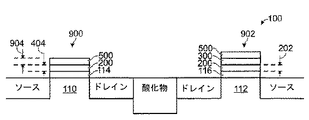
本発明による方法は、金属ゲートスタックを有するデュアルゲートMOSFETを提供し、さらに、このようなMOSFETにおけるしきい値電圧を設定する方法を提供する。本方法は、第1および第2のチャネル領域の上に重なるゲート酸化物層を形成する工程と、ゲート酸化物層の上に重なる第1の厚さを有する第1の金属層を形成する工程と、第1の厚さを有する第1の金属層の上に重なる第2の厚さを有する第2の金属層を形成する工程と、第1のチャネル領域の上に重なる第2の金属層を選択的に除去する工程と、第3の金属層を形成する工程と、第1のチャネル領域の上に重なる第1および第3の金属層の厚さに応じたゲート仕事関数を有する第1のMOSFETを設ける工程と、第2のチャネル領域の上に重なる第1、第2および第3の金属層の厚さの合計に応じたゲート仕事関数を有する第1のMOSFETと相補的な第2のMOSFETを設ける工程とを包含する。
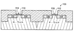
102,104 ソース
106,108 ドレイン
110,112 チャネル
114,116 ゲート絶縁体層
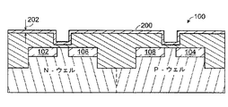
200 第1の金属層
202 第1の厚さ
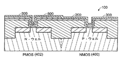
300 第2の金属層
302 第2の厚さ
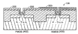
400 NMOSトランジスタ
402 PMOSトランジスタ
404 第3の厚さ
500 第3の金属層
900 第1のゲート
902 第2のゲート
904 第4の厚さ
Claims (44)
- 金属ゲートを有するデュアルゲートMOSFETにおいてしきい値電圧を設定する方法であって、該方法は、
第1および第2のチャネル領域の上に重なるゲート酸化物層を形成する工程と、
該ゲート酸化物層の上に重なる第1の厚さを有する第1の金属層を形成する工程と、
該第1の厚さを有する該第1の金属層の上に重なる第2の厚さを有する第2の金属層を形成する工程と、
該第1のチャネル領域の上に重なる該第2の金属層を選択的に除去する工程と、
該第1のチャネル領域の上に重なる該第1の金属層の厚さに応じたゲート仕事関数を有する第1のMOSFETを設ける工程と、
該第2のチャネル領域の上に重なる該第1の金属層および該第2の金属層の厚さの合計に応じたゲート仕事関数を有する、該第1のMOSFETと相補的な第2のMOSFETを設ける工程と
を包含する、方法。 - 前記第1のチャネル領域の上に重なる前記第1の金属層の厚さに応じたゲート仕事関数を有する第1のMOSFETを設ける工程は、該第1の金属層の第1の厚さに応じてゲート仕事関数を規定する工程を包含し、
前記第2のチャネル領域の上に重なる該第1の金属層および前記第2の金属層の厚さの合計に応じたゲート仕事関数を有する、第1のMOSFETと相補的な第2のMOSFETを設ける工程は、該第1の金属層の第1の厚さおよび該第2の金属層の第2の厚さに応じて、ゲート仕事関数を規定する工程を包含する、請求項1に記載の方法。 - 前記第1のチャネル領域の上に重なる前記第2の金属層を選択的に除去する工程の後に、前記第1の金属層を部分的にエッチングして、該第1のチャネル領域の上に重なり、前記第1の厚さより薄い第3の厚さを有するように第1の金属層を残す工程をさらに包含し、
前記第1のチャネル領域の上に重なる該第1の金属層の厚さに応じたゲート仕事関数を有する第1のMOSFETを設ける工程は、該第1の金属層の第3の厚さに応じてゲート仕事関数を規定する工程を包含する、請求項1に記載の方法。 - 前記第1のチャネル領域の上に重なる前記第1の金属層を部分的にエッチングする工程の後に、該第1のチャネル領域および前記第2のチャネル領域の上に重なる第4の厚さを有する第3の金属層を形成する工程をさらに包含し、
前記第1のチャネル領域の上に重なる該第1の金属層の厚さに応じたゲート仕事関数を有する第1のMOSFETを設ける工程は、該第1および第3の金属層の厚さに応じてゲート仕事関数を規定する工程を包含し、
前記第2のチャネル領域の上に重なる該第1の金属層および前記第2の金属層の厚さの合計に応じたゲート仕事関数を有する、該第1のMOSFETと相補的な第2のMOSFETを設ける工程は、該第1、第2、および第3の金属層の厚さに応じて、ゲート仕事関数を規定する工程を包含する、請求項3に記載の方法。 - 前記第1の金属層を部分的にエッチングして、第3の厚さを有するように第1の金属層を残す工程において、該第3の厚さは、15Å未満であり、
前記第1および第2のチャネル領域の上に重なる第4の厚さを有する第3の金属層を形成する工程において、該第4の厚さは、100Åより厚く、
該第1のチャネル領域の上に重なる、該第1および第3の金属層の厚さに応じてゲート仕事関数を規定する工程は、該第3の金属層の厚さに実質的に応じてゲート仕事関数を規定する工程を包含する、請求項4に記載の方法。 - 前記第1のチャネル領域の上に重なる第2の金属層を選択的に除去する工程の後に、該第1および第2のチャネル領域の上に重なる第4の厚さを有する第3の金属層を形成する工程をさらに包含し、
前記第1のチャネル領域の上に重なる前記第1の金属層の厚さに応じたゲート仕事関数を有する第1のMOSFETを設ける工程は、該第1および第3の金属層の厚さに応じてゲート仕事関数を規定する工程を包含し、
前記第2のチャネル領域の上に重なる該第1の金属層および第2の金属層の厚さの合計に応じたゲート仕事関数を有する、第1のMOSFETと相補的な第2のMOSFETを設ける工程は、該第1、第2、および第3の金属層の厚さに応じてゲート仕事関数を規定する工程を包含する、請求項1に記載の方法。 - 第1の金属層を形成する工程において、該第1の金属層は、低い仕事関数を有し、
第3の金属層を形成する工程において、該第3の金属層は、高い仕事関数を有する、請求項6に記載の方法。 - 第2の金属層を形成する工程において、該第2の金属層は、低い仕事関数を有する、請求項7に記載の方法。
- 低い仕事関数を有する第1の金属層を形成する工程において、該第1の金属層の材料は、単体金属であるW、TiおよびTa、ならびに、二成分金属であるTa−NおよびTi−Nからなる群から選択される材料であり、
高い仕事関数を有する第3の金属層を形成する工程において、該第3の金属層の材料は、単体金属であるIr、PtおよびCu、ならびに、二成分金属であるW−NおよびTi−Nからなる群から選択される材料である、請求項7に記載の方法。 - 第1の金属層を形成する工程において、該第1の金属層は、高い仕事関数を有し、
第3の金属層を形成する工程において、該第3の金属層は、低い仕事関数を有する、請求項6に記載の方法。 - 第2の金属層を形成する工程において、該第2の金属層は、高い仕事関数を有する、請求項10に記載の方法。
- 高い仕事関数を有する第1の金属層を形成する工程において、該第1の金属層の材料は、単体金属であるIr、PtおよびCu、ならびに、二成分金属であるW−NおよびTi−Nからなる群から選択される材料であり、
低い仕事関数を有する第3の金属層を形成する工程において、該第3の金属層の材料は、単体金属であるW、TiおよびTa、ならびに、二成分金属であるTa−NおよびTi−Nからなる群から選択される材料である、請求項11に記載の方法。 - 前記ゲート酸化物層の上に重なる第1の厚さを有する第1の金属層を形成する工程において、該第1の厚さは、約15Å未満であり、
前記第1のチャネル領域の上に重なる該第1の金属層および前記第3の金属層の厚さに応じてゲート仕事関数を規定する工程は、該第3の金属層の厚さに実質的に応じてゲート仕事関数を規定する工程を包含する、請求項6に記載の方法。 - 前記ゲート酸化物層の上に重なる第1の厚さを有する第1の金属層を形成する工程において、該第1の厚さは、約100Åより厚く、
前記第1のチャネル領域の上に重なる該第1の金属層および前記第3の金属層の厚さに応じてゲート仕事関数を規定する工程は、該第1の金属層の厚さに実質的に応じてゲート仕事関数を規定する工程を包含する、請求項6に記載の方法。 - 第4の厚さを有する第3の金属層を形成する工程において、該第3の金属層の該第4の厚さは、100〜1000Åの範囲内である、請求項6に記載の方法。
- 前記第2の金属層を堆積する前に、前記第2のチャネル領域の上に重なるマスクを選択的に堆積する工程をさらに包含し、
前記第1のチャネル領域の上に重なる該第2の金属層を選択的に除去する工程は、該マスクを用いて、該第2のチャネル領域の上に重なる前記第1の金属層を保護する工程を包含する、請求項1に記載の方法。 - 前記ゲート酸化物層の上に重なる第1の金属層を形成する工程は、第1の金属材料から該第1の金属層を形成する工程を包含し、
前記第1の金属層の上に重なる第2の金属層を形成する工程は、該第1の金属材料から該第2の金属層を形成する工程を包含する、請求項16に記載の方法。 - 第1の金属層を形成する工程において、該第1の金属層は、低い仕事関数を有し、
前記第1の金属層の上に重なる第2の金属層を形成する工程において、前記第2の金属層は、高い仕事関数を有する、請求項1に記載の方法。 - 低い仕事関数を有する第1の金属層を形成する工程において、該第1の金属層の材料は、単体金属であるW、Ti、Ta、ならびに、二成分金属であるTa−NおよびTi−Nからなる群から選択される材料であり、
高い仕事関数を有する第2の金属層を形成する工程において、該第2の金属層の材料は、単体金属であるIr、PtおよびCu、ならびに、二成分金属であるW−NおよびTi−Nからなる群から選択される材料である、請求項18に記載の方法。 - 第1の金属層を形成する工程において、該第1の金属層は、高い仕事関数を有し、
前記第1の金属層の上に重なる第2の金属層を形成する工程において、該第2の金属層は、低い仕事関数を有する、請求項1に記載の方法。 - 高い仕事関数を有する第1の金属層を形成する工程において、該第1の金属層の材料は、単体金属であるIr、PtおよびCu、ならびに、二成分金属であるW−NおよびTi−Nからなる群から選択される材料であり、
低い仕事関数を有する第2の金属層を形成する工程において、該第2の金属層の材料は、単体金属であるW、TiおよびTaの単体金属、ならびに、二成分金属であるTa−NおよびTi−Nからなる群から選択される材料である、請求項20に記載の方法。 - 前記ゲート酸化物層の上に重なる第1の厚さを有する第1の金属層を形成する工程において、該第1の厚さは、200Å未満である、請求項1に記載の方法。
- 前記ゲート酸化物層の上に重なる第1の厚さを有する第1の金属層を形成する工程において、該第1の厚さは、約15Åであり、
前記第2のチャネル領域の上に重なる該第1の金属層および前記第2の金属層の厚さに応じてゲート仕事関数を規定する工程は、該第2の金属層の厚さに実質的に応じてゲート仕事関数を規定する工程を包含する、請求項22に記載の方法。 - 前記ゲート酸化物層の上に重なる第1の厚さを有する第1の金属層を形成する工程において、該第1の厚さは、約100Åより厚く、
前記第2のチャネル領域の上に重なる該第1の金属層および前記第2の金属層の厚さに応じてゲート仕事関数を規定する工程は、該第1の金属層の厚さに実質的に応じてゲート仕事関数を規定する工程を包含する、請求項22に記載の方法。 - 前記第1の厚さを有する前記第1の金属層の上に重なる第2の厚さを有する第2の金属層を形成する工程において、該第2の厚さは、100〜1000Åの範囲内である、請求項1に記載の方法。
- 金属ゲートスタックを有するデュアルゲートMOSFETであって、
相補的な第1および第2のチャネル領域の上に重なるゲート酸化物層と、
該ゲート酸化物層の上に重なる第1の金属層と、
該第2のチャネル領域において、該第1の金属層の上に重なる第2の金属層と、
該第1のチャネル領域では該第1の金属層に重なり、該第2のチャネル領域では該第2の金属層の上に重なる第3の金属層と、
該第1および第3の金属層の厚さに応じた仕事関数を有する、該第1のチャネル領域の上に重なる第1のゲートと、
該第1、第2、および第3の金属層の厚さの合計に応じた仕事関数を有する、該第2のチャネル領域の上に重なる第2のゲートと
を備える、デュアルゲートMOSFET。 - 前記第1の金属層は、前記第2のチャネル領域では第1の厚さを有し、前記第1のチャネル領域では該第1の厚さよりも薄い第3の厚さを有する、請求項26に記載のMOSFET。
- 前記第1の金属層の前記第3の厚さは、15Å未満であり、
前記第3の金属層は、100Åより厚い第4の厚さを有し、
前記第1のゲートの仕事関数は、該第3の金属層の該第4の厚さに実質的に応じる、請求項27に記載のMOSFET。 - 前記第1および第2の金属層は、第1の材料から製造される、請求項26に記載のMOSFET。
- 前記第1の金属層は、低い仕事関数を有し、
前記第3の金属層は、高い仕事関数を有する、請求項26に記載のMOSFET。 - 前記第2の金属層は、低い仕事関数を有する、請求項30に記載のMOSFET。
- 前記第1の金属層の材料は、単体金属であるW、TiおよびTa、ならびに、二成分金属であるTa−NおよびTi−Nからなる群から選択される材料であり、
前記第3の金属層の材料は、単体金属であるIr、PtおよびCu、ならびに、二成分金属であるW−NおよびTi−Nからなる群から選択される材料である、請求項30に記載のMOSFET。 - 前記第1の金属層は、高い仕事関数を有し、
前記第3の金属層は、低い仕事関数を有する、請求項26に記載のMOSFET。 - 前記第2の金属層は、高い仕事関数を有する、請求項33に記載のMOSFET。
- 前記第1の金属層の材料は、単体金属であるIr、PtおよびCuの単体金属、ならびに、二成分金属であるW−NおよびTi−Nからなる群から選択される材料であり、
前記第3の金属層の材料は、単体金属であるW、TiおよびTaの単体金属、ならびに、二成分金属であるTa−NおよびTi−Nからなる群から選択される材料である、請求項34に記載のMOSFET。 - 前記第1の金属層は、200Å未満の第1の厚さを有する、請求項26に記載のMOSFET。
- 前記第1の金属層の前記第3の厚さは、約15Å未満であり、
前記第1のゲート仕事関数は、前記第3の金属層の厚さに実質的に応じている、請求項27に記載のMOSFET。 - 前記第1の金属層の前記第3の厚さは、約100Åより厚く、
前記第1のゲート仕事関数は、該第1の金属層の該第3の厚さに実質的に応じている、請求項27に記載のMOSFET。 - 前記第3の金属層の前記第4の厚さは、100〜1000Åの範囲内である、請求項27に記載のMOSFET。
- 前記第1のチャネル領域において、前記第1の金属層と前記一時的な第2の金属層との間に位置する一時的なマスクをさらに備える、請求項26に記載のMOSFET。
- 前記第1の金属層は、低い仕事関数を有し、
前記第2の金属層は、高い仕事関数を有する、請求項26に記載のMOSFET。 - 前記第1の金属層の材料は、単体金属であるW、TiおよびTa、ならびに、二成分金属であるTa−NおよびTi−Nからなる群から選択される材料であり、
前記第2の金属層の材料は、単体金属であるIr、PtおよびCu、ならびに、二成分金属であるW−NおよびTi−Nからなる群から選択される材料である、請求項41に記載のMOSFET。 - 前記第1の金属層は、高い仕事関数を有し、
前記第2の金属層は、低い仕事関数を有する、請求項26に記載のMOSFET。 - 前記第1の金属層の材料は、単体金属であるIr、PtおよびCu、ならびに、二成分金属であるW−NおよびTi−Nからなる群から選択される材料であり、
前記第2の金属層の材料は、単体金属であるW、TiおよびTa、ならびに、二成分金属であるTa−NおよびTi−Nからなる群から選択される材料である、請求項43に記載のMOSFET。
Applications Claiming Priority (1)
| Application Number | Priority Date | Filing Date | Title |
|---|---|---|---|
| US10/376,795 US6873048B2 (en) | 2003-02-27 | 2003-02-27 | System and method for integrating multiple metal gates for CMOS applications |
Publications (1)
| Publication Number | Publication Date |
|---|---|
| JP2004260165A true JP2004260165A (ja) | 2004-09-16 |
Family
ID=32908003
Family Applications (1)
| Application Number | Title | Priority Date | Filing Date |
|---|---|---|---|
| JP2004039093A Pending JP2004260165A (ja) | 2003-02-27 | 2004-02-16 | Cmosに適用する複数の金属ゲートを集積するシステムおよび方法 |
Country Status (4)
| Country | Link |
|---|---|
| US (1) | US6873048B2 (ja) |
| JP (1) | JP2004260165A (ja) |
| KR (1) | KR100695640B1 (ja) |
| TW (1) | TWI230440B (ja) |
Cited By (10)
| Publication number | Priority date | Publication date | Assignee | Title |
|---|---|---|---|---|
| JP2005347705A (ja) * | 2004-06-07 | 2005-12-15 | Samsung Electronics Co Ltd | 半導体装置 |
| JP2006245324A (ja) * | 2005-03-03 | 2006-09-14 | Toshiba Corp | 半導体装置及びその製造方法 |
| JP2006324342A (ja) * | 2005-05-17 | 2006-11-30 | Renesas Technology Corp | 半導体装置およびその製造方法 |
| JP2006351580A (ja) * | 2005-06-13 | 2006-12-28 | Sony Corp | 半導体装置および半導体装置の製造方法 |
| JP2007123867A (ja) * | 2005-09-30 | 2007-05-17 | Infineon Technologies Ag | 半導体デバイスおよびその製造方法 |
| JP2009164207A (ja) * | 2007-12-28 | 2009-07-23 | Toshiba Corp | 半導体装置及びその製造方法 |
| JP2010027716A (ja) * | 2008-07-16 | 2010-02-04 | Tokyo Electron Ltd | 半導体装置及び半導体装置の製造方法 |
| US8178902B2 (en) | 2004-06-17 | 2012-05-15 | Infineon Technologies Ag | CMOS transistor with dual high-k gate dielectric and method of manufacture thereof |
| US8399934B2 (en) | 2004-12-20 | 2013-03-19 | Infineon Technologies Ag | Transistor device |
| US8946026B2 (en) | 2010-11-24 | 2015-02-03 | Samsung Electronics Co., Ltd. | Methods of fabricating a semiconductor device including metal gate electrodes |
Families Citing this family (26)
| Publication number | Priority date | Publication date | Assignee | Title |
|---|---|---|---|---|
| JP2004351658A (ja) * | 2003-05-27 | 2004-12-16 | Toyoda Gosei Co Ltd | 分岐パイプの製造方法 |
| US6967131B2 (en) * | 2003-10-29 | 2005-11-22 | International Business Machines Corp. | Field effect transistor with electroplated metal gate |
| US20050250258A1 (en) * | 2004-05-04 | 2005-11-10 | Metz Matthew V | Method for making a semiconductor device having a high-k gate dielectric layer and a metal gate electrode |
| US7126199B2 (en) * | 2004-09-27 | 2006-10-24 | Intel Corporation | Multilayer metal gate electrode |
| JP2006156807A (ja) * | 2004-11-30 | 2006-06-15 | Toshiba Corp | 半導体装置およびその製造方法 |
| KR100706244B1 (ko) * | 2005-04-07 | 2007-04-11 | 삼성전자주식회사 | 반도체 장치 및 그 제조 방법 |
| US7361538B2 (en) * | 2005-04-14 | 2008-04-22 | Infineon Technologies Ag | Transistors and methods of manufacture thereof |
| CN1924870A (zh) * | 2005-09-02 | 2007-03-07 | 鸿富锦精密工业(深圳)有限公司 | 自动选取金属氧化物半导体场效应晶体管的系统及方法 |
| US20070052037A1 (en) * | 2005-09-02 | 2007-03-08 | Hongfa Luan | Semiconductor devices and methods of manufacture thereof |
| US20070052036A1 (en) * | 2005-09-02 | 2007-03-08 | Hongfa Luan | Transistors and methods of manufacture thereof |
| US7495290B2 (en) * | 2005-12-14 | 2009-02-24 | Infineon Technologies Ag | Semiconductor devices and methods of manufacture thereof |
| US7510943B2 (en) * | 2005-12-16 | 2009-03-31 | Infineon Technologies Ag | Semiconductor devices and methods of manufacture thereof |
| US7944006B2 (en) * | 2008-01-15 | 2011-05-17 | International Business Machines Corporation | Metal gate electrode stabilization by alloying |
| JP5104373B2 (ja) * | 2008-02-14 | 2012-12-19 | 日本ゼオン株式会社 | 位相差板の製造方法 |
| US20090206416A1 (en) * | 2008-02-19 | 2009-08-20 | International Business Machines Corporation | Dual metal gate structures and methods |
| US7790553B2 (en) * | 2008-07-10 | 2010-09-07 | International Business Machines Corporation | Methods for forming high performance gates and structures thereof |
| US9269634B2 (en) | 2011-05-16 | 2016-02-23 | Globalfoundries Inc. | Self-aligned metal gate CMOS with metal base layer and dummy gate structure |
| CN103531540B (zh) * | 2012-07-02 | 2016-06-08 | 中国科学院微电子研究所 | 半导体器件制造方法 |
| CN103579113B (zh) * | 2012-08-03 | 2017-02-08 | 中国科学院微电子研究所 | 具有双功函数金属栅的互补场效应晶体管及其制造方法 |
| CN103681802B (zh) * | 2012-09-18 | 2016-09-14 | 中国科学院微电子研究所 | 一种半导体结构及其制作方法 |
| CN103681801A (zh) * | 2012-09-18 | 2014-03-26 | 中国科学院微电子研究所 | 一种半导体结构及其制作方法 |
| CN104134691B (zh) * | 2013-05-03 | 2017-09-08 | 中国科学院微电子研究所 | 半导体器件及其制造方法 |
| KR102128450B1 (ko) * | 2013-11-12 | 2020-06-30 | 에스케이하이닉스 주식회사 | 트랜지스터의 문턱전압조절을 위한 방법 및 게이트구조물 |
| US9117908B2 (en) * | 2013-12-16 | 2015-08-25 | Globalfoundries Inc. | Methods of forming replacement gate structures for semiconductor devices and the resulting semiconductor products |
| CN108122844B (zh) | 2016-11-30 | 2020-06-09 | 中芯国际集成电路制造(上海)有限公司 | 半导体结构的形成方法 |
| US11264289B2 (en) | 2019-07-11 | 2022-03-01 | Tokyo Electron Limited | Method for threshold voltage tuning through selective deposition of high-K metal gate (HKMG) film stacks |
Citations (5)
| Publication number | Priority date | Publication date | Assignee | Title |
|---|---|---|---|---|
| JPH0846057A (ja) * | 1994-07-28 | 1996-02-16 | Sony Corp | Nmosトランジスタとpmosトランジスタとを有する半導体装置及びその製造方法 |
| JP2000243853A (ja) * | 1999-02-19 | 2000-09-08 | Nec Corp | Mis型電界効果トランジスタ及びその製造方法 |
| JP2000315789A (ja) * | 1999-04-30 | 2000-11-14 | Toshiba Corp | 半導体装置及びその製造方法 |
| US6410376B1 (en) * | 2001-03-02 | 2002-06-25 | Chartered Semiconductor Manufacturing Ltd. | Method to fabricate dual-metal CMOS transistors for sub-0.1 μm ULSI integration |
| JP2003273350A (ja) * | 2002-03-15 | 2003-09-26 | Nec Corp | 半導体装置及びその製造方法 |
Family Cites Families (4)
| Publication number | Priority date | Publication date | Assignee | Title |
|---|---|---|---|---|
| US6166417A (en) * | 1998-06-30 | 2000-12-26 | Intel Corporation | Complementary metal gates and a process for implementation |
| US6373111B1 (en) * | 1999-11-30 | 2002-04-16 | Intel Corporation | Work function tuning for MOSFET gate electrodes |
| US6511911B1 (en) * | 2001-04-03 | 2003-01-28 | Advanced Micro Devices, Inc. | Metal gate stack with etch stop layer |
| KR100399356B1 (ko) * | 2001-04-11 | 2003-09-26 | 삼성전자주식회사 | 듀얼 게이트를 가지는 씨모스형 반도체 장치 형성 방법 |
-
2003
- 2003-02-27 US US10/376,795 patent/US6873048B2/en not_active Expired - Fee Related
-
2004
- 2004-02-16 JP JP2004039093A patent/JP2004260165A/ja active Pending
- 2004-02-24 TW TW093104619A patent/TWI230440B/zh not_active IP Right Cessation
- 2004-02-27 KR KR1020040013347A patent/KR100695640B1/ko not_active Expired - Fee Related
Patent Citations (5)
| Publication number | Priority date | Publication date | Assignee | Title |
|---|---|---|---|---|
| JPH0846057A (ja) * | 1994-07-28 | 1996-02-16 | Sony Corp | Nmosトランジスタとpmosトランジスタとを有する半導体装置及びその製造方法 |
| JP2000243853A (ja) * | 1999-02-19 | 2000-09-08 | Nec Corp | Mis型電界効果トランジスタ及びその製造方法 |
| JP2000315789A (ja) * | 1999-04-30 | 2000-11-14 | Toshiba Corp | 半導体装置及びその製造方法 |
| US6410376B1 (en) * | 2001-03-02 | 2002-06-25 | Chartered Semiconductor Manufacturing Ltd. | Method to fabricate dual-metal CMOS transistors for sub-0.1 μm ULSI integration |
| JP2003273350A (ja) * | 2002-03-15 | 2003-09-26 | Nec Corp | 半導体装置及びその製造方法 |
Cited By (20)
| Publication number | Priority date | Publication date | Assignee | Title |
|---|---|---|---|---|
| JP2005347705A (ja) * | 2004-06-07 | 2005-12-15 | Samsung Electronics Co Ltd | 半導体装置 |
| US8178902B2 (en) | 2004-06-17 | 2012-05-15 | Infineon Technologies Ag | CMOS transistor with dual high-k gate dielectric and method of manufacture thereof |
| US9269635B2 (en) | 2004-06-17 | 2016-02-23 | Infineon Technologies Ag | CMOS Transistor with dual high-k gate dielectric |
| US8729633B2 (en) | 2004-06-17 | 2014-05-20 | Infineon Technologies Ag | CMOS transistor with dual high-k gate dielectric |
| US8637357B2 (en) | 2004-06-17 | 2014-01-28 | Infineon Technologies Ag | CMOS Transistor with dual high-k gate dielectric and method of manufacture thereof |
| US8476678B2 (en) | 2004-06-17 | 2013-07-02 | Infineon Technologies Ag | CMOS Transistor with dual high-k gate dielectric |
| US8669154B2 (en) | 2004-12-20 | 2014-03-11 | Infineon Technologies Ag | Transistor device and method of manufacture thereof |
| US8399934B2 (en) | 2004-12-20 | 2013-03-19 | Infineon Technologies Ag | Transistor device |
| JP2006245324A (ja) * | 2005-03-03 | 2006-09-14 | Toshiba Corp | 半導体装置及びその製造方法 |
| US7718521B2 (en) | 2005-03-03 | 2010-05-18 | Kabushiki Kaisha Toshiba | Semiconductor device and method for manufacturing the same |
| US8148787B2 (en) | 2005-03-03 | 2012-04-03 | Kabushiki Kaisha Toshiba | Semiconductor device and method for manufacturing the same |
| JP2006324342A (ja) * | 2005-05-17 | 2006-11-30 | Renesas Technology Corp | 半導体装置およびその製造方法 |
| JP2006351580A (ja) * | 2005-06-13 | 2006-12-28 | Sony Corp | 半導体装置および半導体装置の製造方法 |
| US8722473B2 (en) | 2005-09-30 | 2014-05-13 | Infineon Technologies Ag | Semiconductor devices and methods of manufacture thereof |
| US8188551B2 (en) | 2005-09-30 | 2012-05-29 | Infineon Technologies Ag | Semiconductor devices and methods of manufacture thereof |
| JP2007123867A (ja) * | 2005-09-30 | 2007-05-17 | Infineon Technologies Ag | 半導体デバイスおよびその製造方法 |
| US9659962B2 (en) | 2005-09-30 | 2017-05-23 | Infineon Technologies Ag | Semiconductor devices and methods of manufacture thereof |
| JP2009164207A (ja) * | 2007-12-28 | 2009-07-23 | Toshiba Corp | 半導体装置及びその製造方法 |
| JP2010027716A (ja) * | 2008-07-16 | 2010-02-04 | Tokyo Electron Ltd | 半導体装置及び半導体装置の製造方法 |
| US8946026B2 (en) | 2010-11-24 | 2015-02-03 | Samsung Electronics Co., Ltd. | Methods of fabricating a semiconductor device including metal gate electrodes |
Also Published As
| Publication number | Publication date |
|---|---|
| KR20040077528A (ko) | 2004-09-04 |
| KR100695640B1 (ko) | 2007-03-15 |
| TWI230440B (en) | 2005-04-01 |
| TW200425413A (en) | 2004-11-16 |
| US20040171222A1 (en) | 2004-09-02 |
| US6873048B2 (en) | 2005-03-29 |
Similar Documents
| Publication | Publication Date | Title |
|---|---|---|
| JP2004260165A (ja) | Cmosに適用する複数の金属ゲートを集積するシステムおよび方法 | |
| US6894353B2 (en) | Capped dual metal gate transistors for CMOS process and method for making the same | |
| US7229873B2 (en) | Process for manufacturing dual work function metal gates in a microelectronics device | |
| JP4513087B2 (ja) | 金属ゲートスタック制御を伴うmosfetしきい値電圧調整 | |
| JP4624782B2 (ja) | Mosトランジスタ及びその形成方法 | |
| US7250658B2 (en) | Hybrid planar and FinFET CMOS devices | |
| US7109079B2 (en) | Metal gate transistor CMOS process and method for making | |
| CN102388451B (zh) | 形成半导体器件的方法 | |
| US6864163B1 (en) | Fabrication of dual work-function metal gate structure for complementary field effect transistors | |
| US7253050B2 (en) | Transistor device and method of manufacture thereof | |
| US10170373B2 (en) | Methods for making robust replacement metal gates and multi-threshold devices in a soft mask integration scheme | |
| JP2007208260A (ja) | 二重仕事関数金属ゲートスタックを備えるcmos半導体装置 | |
| JP2009545168A (ja) | ゲート誘電体上に完全シリサイド化(fusi)ゲート電極を選択的に形成する方法、及びその完全シリサイド化ゲート電極を有する半導体デバイス | |
| US7297598B2 (en) | Process for erase improvement in a non-volatile memory device | |
| JP2008166713A (ja) | 複数の誘電体を備えた半導体装置の製造方法 | |
| US8486786B2 (en) | Enhancing uniformity of a channel semiconductor alloy by forming STI structures after the growth process | |
| CN102110689A (zh) | 一种半导体器件及其制造方法 | |
| JP5669752B2 (ja) | チャネル半導体合金を備えたトランジスタにおける堆積不均一性の低減によるスレッショルド電圧ばらつきの低減 | |
| US20070059874A1 (en) | Dual Metal Gate and Method of Manufacture | |
| US20080233695A1 (en) | Integration method of inversion oxide (TOXinv) thickness reduction in CMOS flow without added pattern | |
| US7018887B1 (en) | Dual metal CMOS transistors with silicon-metal-silicon stacked gate electrode | |
| US7638395B2 (en) | Semiconductor device fabricating method | |
| US6822291B2 (en) | Optimized gate implants for reducing dopant effects during gate etching | |
| JP2009010417A (ja) | 半導体装置の製造方法 | |
| US6599802B2 (en) | Low-voltage-Vt (CMOS) transistor design using a single mask and without any additional implants by way of tailoring the effective channel length (Leff) |
Legal Events
| Date | Code | Title | Description |
|---|---|---|---|
| A621 | Written request for application examination |
Free format text: JAPANESE INTERMEDIATE CODE: A621 Effective date: 20060125 |
|
| A131 | Notification of reasons for refusal |
Free format text: JAPANESE INTERMEDIATE CODE: A131 Effective date: 20100212 |
|
| A521 | Request for written amendment filed |
Free format text: JAPANESE INTERMEDIATE CODE: A523 Effective date: 20100413 |
|
| A131 | Notification of reasons for refusal |
Free format text: JAPANESE INTERMEDIATE CODE: A131 Effective date: 20110512 |
|
| A02 | Decision of refusal |
Free format text: JAPANESE INTERMEDIATE CODE: A02 Effective date: 20110909 |