JP2004281161A - Adhesive connector and manufacturing method thereof - Google Patents
Adhesive connector and manufacturing method thereof Download PDFInfo
- Publication number
- JP2004281161A JP2004281161A JP2003069284A JP2003069284A JP2004281161A JP 2004281161 A JP2004281161 A JP 2004281161A JP 2003069284 A JP2003069284 A JP 2003069284A JP 2003069284 A JP2003069284 A JP 2003069284A JP 2004281161 A JP2004281161 A JP 2004281161A
- Authority
- JP
- Japan
- Prior art keywords
- thin film
- metal thin
- adhesive layer
- pressure
- sensitive adhesive
- Prior art date
- Legal status (The legal status is an assumption and is not a legal conclusion. Google has not performed a legal analysis and makes no representation as to the accuracy of the status listed.)
- Granted
Links
Images

Landscapes
- Coupling Device And Connection With Printed Circuit (AREA)
Abstract
【課題】複雑な信号線を持つプリント配線基板間同士を容易に接続できて高品質な高速伝送化が可能であり、しかも低背化を維持した上で十分に狭ピッチ化を具現し得る粘着式コネクタを提供すること。
【解決手段】この粘着式コネクタ1は、第1の粘着剤層3により基材2とグランドプレートとなる接地金属板層4との間を固着すると共に、第2の粘着剤層5の一方の面に接地金属板層4を固着し、且つ他方の面に複数の端子部を固着配設して成り、複数の端子部は、第2の粘着剤層5の他方の面の周縁箇所に形成された貫通穴7における端縁間で層両面部分へ跨がるように金属薄膜により形成されると共に、少なくとも一つのものが接地金属板層4に対して接続された接地用金属薄膜6と、第2の粘着剤層5の他方の面の接地用金属薄膜6と隔てた箇所に互いに平行となるように列設された信号用金属薄膜8とから成る。
【選択図】 図1An adhesive capable of easily connecting printed wiring boards having complicated signal lines to achieve high-quality, high-speed transmission, and realizing a sufficiently narrow pitch while maintaining a low profile. To provide a type connector.
The adhesive connector (1) secures a base (2) and a ground metal plate layer (4) serving as a ground plate with a first adhesive layer (3), and one of a second adhesive layer (5). The ground metal plate layer 4 is fixed to the surface, and a plurality of terminal portions are fixedly arranged on the other surface. The plurality of terminal portions are formed at the periphery of the other surface of the second adhesive layer 5. A ground metal thin film 6 formed of a metal thin film so as to straddle both sides of the layer between the edges of the formed through hole 7 and at least one of which is connected to the ground metal plate layer 4; A signal metal thin film 8 arranged in parallel with each other at a position separated from the ground metal thin film 6 on the other surface of the second adhesive layer 5.
[Selection diagram] Fig. 1
Description
【0001】
【発明の属する技術分野】
本発明は、主として粘着剤層に配設された複数の端子部を2つの離間されたプリント配線基板表面上の配線部分に対して粘着作用により直接的に接続可能な構造を持つ粘着式コネクタであって、詳しくはマイクロストリップライン構造を有して高速伝送に好適な粘着式コネクタ及びその製造方法に関する。
【0002】
【従来の技術】
従来、一般的なプリント配線基板における表面上の配線部分に対してフレキシブルプリント配線基板(FPC)を接続する場合、FPCケーブルの端部に配線数分を接触可能な金属バネによるコンタクトを持つコネクタを用い、このコネクタをプリント配線基板表面の配線部分に半田付けした後、コネクタ及びFPCケーブルを着脱するようにしたもの(例えば特許文献1参照)、或いはプリント配線基板上に実装された集積回路素子の背面に接続固定された接続ブロックの係合凹所にFPCケーブルを接続したコネクタを挿入してコネクタのコンタクトを集積回路素子の背面電極に接触させるようにしたもの(特許文献2参照)等が挙げられる。
【0003】
ところが、こうしたコネクタは、何れもFPC本体とは別品で構成されるため、部品点数が多くなり、簡単に接続を行うことができないという不便がある上、接続部品間全体の低背化に適さないという難点がある。
【0004】
そこで、こうした問題を解決可能であると共に、技術的に別途な試みとしてFPC自体の基本構造を工夫し、粘着剤や接着剤上へ導体パターンを形成した上で機械的結合手段として各種用途に利用できるようにしたもの、特に粘着式コネクタとする場合には基材の一面上に配された粘着剤上に複数の導体パターンを互いに平行に所定のピッチで配列した構成のもの(特許文献3参照)が本出願人により提案されている。
【0005】
更に、転写の歩留まりを向上させ、接触時の抵抗値のバラツキを低減できる電気接続部材も本出願人により提案されているが、この電気接続部材は、金属薄膜を基材の一面の粘着剤に転写して粘着剤上に配線パターンを形成したもの(特許文献4参照)で、粘着による接続が不向きな箇所への接続を可能にした一例として、FPCに電気接続部材の配線パターンを粘着剤の粘着作用により直接的に接続した構成の粘着式コネクタが開示されている。
【0006】
【特許文献1】
特開平9−82427号公報(要約)
【0007】
【特許文献2】
特開2001−313109号公報(要約、第3頁)
【0008】
【特許文献3】
特開2001−210933号公報(要約、第5頁、図4)
【0009】
【特許文献4】
特開2002−184546号公報(要約、第4頁、図6)
【0010】
【発明が解決しようとする課題】
上述した特許文献3や特許文献4に開示された粘着式コネクタの場合、それ以前のFPC用コネクタ(FPCケーブルに結合される別体のコネクタを要するもの)と比べれば部品点数が少なくて簡単に接続を行うことができ、しかも接続部品間全体の低背化を十分に具現できると共に、狭ピッチ化による高速伝送も或る程度まで具現できるが、粘着剤上に形成される配線パターンが複数の平行なライン状のみの構造であるため、最近の複雑な中央演算処理装置(CPU)や大規模集積回路(LSI)等が多数搭載される複雑な信号線を持つプリント配線基板間の同士を接続しての高速伝送化への適用には困難がある他、低背化を維持した上で十分に狭ピッチ化を具現し難いという問題がある。
【0011】
本発明は、このような問題点を解決すべくなされたもので、その技術的課題は、複雑な信号線を持つプリント配線基板間同士を容易に接続できて高品質な高速伝送化が可能であり、しかも低背化を維持した上で十分に狭ピッチ化を具現し得る粘着式コネクタ及びその製造方法を提供することにある。
【0012】
【課題を解決するための手段】
本発明によれば、絶縁性の基材に対して薄い金属導電板から成るグランドプレートと粘着剤層とが積層され、且つ該粘着剤層に複数の端子部を少なくとも一つのものが該グランドプレートに接続されるように固着配設されて成る粘着式コネクタにおいて、粘着剤層は、第1の粘着剤層及び第2の粘着剤層を含んでおり、第1の粘着剤層により基材とグランドプレートとの間を固着すると共に、第2の粘着剤層の一方の面に該グランドプレートを固着し、且つ他方の面に複数の端子部を固着配設して成り、更に、複数の端子部は、第2の粘着剤層の他方の面の周縁箇所に形成された貫通穴における端縁間で層両面部分へ跨がるように金属薄膜により形成されると共に、少なくとも一つのものがグランドプレートに対して接続された接地用金属薄膜と、第2の粘着剤層の他方の面の接地用金属薄膜と隔てた箇所に互いに平行となるように列設された信号用金属薄膜とから成る粘着式コネクタが得られる。
【0013】
又、本発明によれば、上記粘着式コネクタにおいて、信号用金属薄膜は、接地用金属薄膜及びグランドプレートに対してマイクロストリップライン構造を成してインピーダンスがマッチングされており、信号用金属薄膜及び接地用金属薄膜は、2つの離間されたプリント配線基板表面上の所定箇所にあっての配線部分に対して第2の粘着剤層の粘着作用により直接的に接続される構造である粘着式コネクタが得られる。
【0014】
更に、本発明によれば、薄い金属導電板から成るグランドプレート上に粘着剤により第2の粘着剤層を堆積する粘着剤堆積工程と、グランドプレートの表面側から周縁部の所定箇所に穴あけして貫通穴を形成する穴あけ工程と、第2の粘着剤層の表面側から貫通穴の端縁間に対して層両面部分へ跨がるように金属薄膜により端子部としての接地用金属薄膜を転写して折り曲げ形成する第1の金属薄膜転写工程と、第2の粘着剤層の表面に対して接地用金属薄膜と隔てた箇所に互いに平行となるように金属薄膜により端子部としての信号用金属薄膜を該接地用金属薄膜及びグランドプレートに対してマイクロストリップライン構造を成すように転写して列状に形成する第2の金属薄膜転写工程と、グランドプレートの表面に粘着剤シートを貼布して第1の粘着剤層を形成した後、該第1の粘着剤層の表面に絶縁性の基材シートを貼布して基材を形成する粘着剤シート及び基材シート貼布工程とを有する粘着式コネクタの製造方法が得られる。
【0015】
【発明の実施の形態】
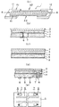
以下に本発明の実施の形態について、図面を参照して詳細に説明する。図1は、本発明の一つの実施の形態に係る粘着式コネクタ1の基本構造及び粘着機能を示したもので、同図(a)は粘着式コネクタ1を2つの離間されたプリント配線基板11,12表面上の所定箇所にあっての配線部分に対して粘着作用により接続した状態を示す外観斜視図に関するもの,同図(b)は同図(a)に示される粘着式コネクタ1のA1−A1線方向における要部の側面断面図に関するもの,同図(c)は同図(a)に示される粘着式コネクタ1のA2−A2線方向における要部の側面断面図に関するもの,同図(d)は同図(a)に示される粘着式コネクタ1のB−B線方向における一部を破断した要部の側面断面図に関するもの,同図(e)は同図(a)に示される粘着式コネクタ1の接着面(裏面)にあっての一部を破断した要部の平面図に関するものである。
【0016】
この粘着式コネクタ1は、絶縁性の基材2に対して薄い金属導電板から成るグランドプレートとなる接地金属板層4と粘着剤層3,5とを積層し、且つ粘着剤層5に複数の端子部を少なくとも一つのものが接地金属板層4に接続されるように固着配設して成るもので、図1(a)に示されるように、2つの離間されたプリント配線基板11,12表面上の所定箇所にあっての配線部分に対して粘着剤層5の粘着作用により直接的に各端子部を接続可能な構造となっている。
【0017】
図1(b)〜(e)を参照して具体的に説明すれば、粘着剤層3,5は、第1の粘着剤層3及び第2の粘着剤層5に区別され、第1の粘着剤層3により基材2とグランドプレートとなる接地金属板層4との間を固着すると共に、第2の粘着剤層5の一方の面に接地金属板層4を固着し、且つ他方の面に複数の端子部を固着配設して成るもので、更に、複数の端子部は、第2の粘着剤層5の他方の面の周縁箇所に形成された貫通穴7における端縁間で層両面部分へ跨がるように金属薄膜により形成されると共に、少なくとも一つのものが接地金属板層4に対して接続された接地用金属薄膜6と、第2の粘着剤層5の他方の面の接地用金属薄膜6と隔てた箇所に互いに平行となるように列設された信号用金属薄膜8とから成っている。
【0018】
即ち、ここでの信号用金属薄膜8は、接地用金属薄膜6及び接地金属板層4(グランド部分)に対して略同軸状のマイクロストリップライン構造を成してインピーダンスがマッチングされている。又、信号用金属薄膜8及び接地用金属薄膜6は、2つの離間されたプリント配線基板11,12表面上の所定箇所にあっての配線部分に対して第2の粘着剤層5の粘着作用により直接的に接続される構造となっている。
【0019】
このような構造の粘着式コネクタ1の場合、粘着剤層3,5により接地用金属薄膜6が接地金属板層4に対して常に密着した状態で保持されており、各信号用金属薄膜8が接地用金属薄膜6及び接地金属板層4に対してマイクロストリップライン構造を成してインピーダンスがマッチングされた上で各プリント配線基板11,12への粘着作用による接続が直接的に行われるため、各プリント配線基板11,12が複雑な信号線を持つ場合でも、各プリント配線基板11,12間同士を容易に接続できて高品質な高速伝送化が可能となり、しかも低背化を維持した上で十分に狭ピッチ化を図ることができる。特に、各プリント配線基板11,12がFPCである場合には粘着式コネクタ1を接続した後で各プリント配線基板11,12を板面方向で幾分曲げても、電気的な接続状態が十分安定して保持される。
【0020】
ところで、この粘着式コネクタ1における各部材料として、基材2にはポリエステル,ポリイミド等のフィルムシート、粘着剤層3,5の粘着剤にはSi系,アクリル系の材料を用いる場合を例示できる。接地用金属薄膜6及び信号用金属薄膜8の形成は、Siウェハー上にスパッタリング等で金属薄膜を堆積させてから粘着シートを貼り付けて金属薄膜を転写させれば良く、接地用金属薄膜6は貫通穴7の端縁間で層両面部分へ跨がるように折り曲げられた形状で形成される。何れにしても、これらの金属薄膜は非常に滑らかで膜厚が薄いものである。
【0021】
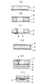
次に、このような粘着式コネクタ1の製造方法について説明する。図2は、粘着式コネクタ1の製造過程を工程別に示した要部の側面断面図であり、同図(a)は粘着剤堆積工程に関するもの,同図(b)は穴あけ工程に関するもの,同図(c)は第1の金属薄膜転写工程に関するもの,同図(d)は第2の金属薄膜転写工程に関するもの,同図(e)は粘着剤シート及び基材シート貼布工程に関するもの,同図(d)は同図(e)の粘着剤シート及び基材シート貼布工程後の局部の拡大図に関するものである。
【0022】
即ち、粘着式コネクタ1を製造する場合、先ず図2(a)に示されるような粘着剤堆積工程として、グランドプレートとなる薄い金属導電板から成る接地金属板層4上に粘着剤により第2の粘着剤層5を堆積した後、図2(b)に示されるような穴あけ工程として、第2の粘着剤層5の表面にセパレータ9を貼布した状態で接地金属板層4の表面側から周縁部の所定箇所に機械加工又はレーザー加工により穴あけして貫通穴7を形成する。
【0023】
次に、図2(c)に示されるような第1の金属薄膜転写工程として、第2の粘着剤層5の表面からセパレータ9を剥がした状態で第2の粘着剤層5の表面側から貫通穴7の端縁間に対して層両面部分へ跨がるように金属薄膜により端子部としての接地用金属薄膜6を転写して折り曲げ形成する。この後、図2(d)に示されるような第2の金属薄膜転写工程として、第2の粘着剤層5の表面に対して接地用金属薄膜6と隔てた箇所に互いに平行となるように、金属薄膜により端子部としての信号用金属薄膜8を接地用金属薄膜6及び接地金属板層4に対してマイクロストリップライン構造を成すように転写して列状に形成する。
【0024】
更に、図2(e)に示されるような粘着剤シート及び基材シート貼布工程として、第2の粘着剤層5の表面にセパレータ10を貼布した状態で接地金属板層4の表面に粘着剤シートを貼布して第1の粘着剤層3を形成した後、第1の粘着剤層3の表面に絶縁性の基材シートを貼布して基材2を形成する。尚、第1の粘着剤層3と基材2とは、別々に貼布した場合で説明したが、粘着剤層付きの基材シート(第1の粘着剤層3と基材2とを一体化したもの)を用いても良い。この状態では、図2(f)に示されるように、接地用金属薄膜6の一部が接地金属板層4に対して十分に密着保持された状態となっている。
【0025】
図3は、このようにして得られた粘着式コネクタ1のプリント配線基板13表面上の所定箇所にあっての配線部分に対する粘着作用による接続状態の細部構造の要部を一部を破断して示した側面断面図である。
【0026】
ここでは、先の製造過程を経て得られた粘着式コネクタ1の第2の粘着剤層5の表面からセパレータ10を剥がし、プリント配線基板13表面上の所定箇所にあっての配線部分であるグランドランド,シグナルランドにそれぞれ第2の粘着剤層5の表面の接地用金属薄膜6,信号用金属薄膜8をその周囲の粘着剤の粘着作用により接続した状態を示しており、十分に安定した電気的接触が図られると共に、信号用金属薄膜8が接地用金属薄膜6及び接地金属板層4に対してマイクロストリップライン構造を成していることによりトンネル電流による導通が得られることを示している。
【0027】
【発明の効果】
以上に説明したように、本発明の粘着式コネクタによれば、従来の粘着式コネクタにおける粘着剤上に形成された複数の平行なライン状のみの配線パターン構造を改良し、第1の粘着剤層により基材とグランドプレートとの間を固着すると共に、第2の粘着剤層の一方の面にグランドプレートを固着し、且つ他方の面に複数の端子部を固着配設する構成において、複数の端子部として第2の粘着剤層の他方の面の周縁箇所に形成された貫通穴における端縁間で層両面部分へ跨がるように金属薄膜により形成されると共に、少なくとも一つのものがグランドプレートに対して接続された接地用金属薄膜と、第2の粘着剤層の他方の面の接地用金属薄膜と隔てた箇所に互いに平行となるように列設された信号用金属薄膜とを有する構造としているため、プリント配線基板表面上の所定箇所にあっての配線部分に第2の粘着剤層の表面の接地用金属薄膜及び信号用金属薄膜をその周囲の粘着剤の粘着作用により直接的に簡単に接続することができ、十分に安定した電気的接触が得られるようになる。結果として、従来品とは異なり、プリント配線基板が複雑な信号線を持つ場合でも、プリント配線基板間同士を容易に接続できて高品質な高速伝送化が可能となり、しかも低背化を維持した上で十分に狭ピッチ化を図り得るようになる。
【図面の簡単な説明】
【図1】本発明の一つの実施の形態に係る粘着式コネクタの基本構造及び粘着機能を示したもので、(a)は粘着式コネクタを2つの離間されたプリント配線基板表面上の所定箇所にあっての配線部分に対して粘着作用により接続した状態を示す外観斜視図に関するもの,(b)は(a)に示される粘着式コネクタのA1−A1線方向における要部の側面断面図に関するもの,(c)は(a)に示される粘着式コネクタのA2−A2線方向における要部の側面断面図に関するもの,(d)は(a)に示される粘着式コネクタのB−B線方向における一部を破断した要部の側面断面図に関するもの,(e)は(a)に示される粘着式コネクタの接着面(裏面)にあっての一部を破断した要部の平面図に関するものである。
【図2】図1に示す粘着式コネクタの製造過程を工程別に示した要部の側面断面図であり、(a)は粘着剤堆積工程に関するもの,(b)は穴あけ工程に関するもの,(c)は第1の金属薄膜転写工程に関するもの,(d)は第2の金属薄膜転写工程に関するもの,(e)は粘着剤シート及び基材シート貼布工程に関するもの,(f)は(e)の粘着剤シート及び基材シート貼布工程後の局部の拡大図に関するものである。
【図3】図1に示す粘着式コネクタのプリント配線基板表面上の所定箇所にあっての配線部分に対する粘着作用による接続状態の細部構造の要部を一部を破断して示した側面断面図である。
【符号の説明】
1 粘着式コネクタ
2 基材
3,5 粘着剤層
4 接地金属板層
6 接地用金属薄膜
7 貫通穴
8 信号用金属薄膜
9,10 セパレータ
11,12,13 プリント配線基板[0001]
TECHNICAL FIELD OF THE INVENTION
The present invention relates to an adhesive connector having a structure capable of directly connecting a plurality of terminal portions provided on an adhesive layer directly to wiring portions on two separated printed wiring board surfaces by an adhesive action. More specifically, the present invention relates to an adhesive connector having a microstrip line structure and suitable for high-speed transmission, and a method of manufacturing the same.
[0002]
[Prior art]
2. Description of the Related Art Conventionally, when a flexible printed circuit board (FPC) is connected to a wiring portion on a surface of a general printed circuit board, a connector having a metal spring contact capable of contacting the end of the FPC cable by the number of wires is used. After the connector is soldered to the wiring portion on the surface of the printed wiring board, the connector and the FPC cable are attached / detached (for example, see Patent Document 1), or an integrated circuit element mounted on the printed wiring board is used. One in which a connector to which an FPC cable is connected is inserted into an engagement recess of a connection block fixedly connected to the back surface so that the contact of the connector comes into contact with the back electrode of the integrated circuit element (see Patent Document 2). Can be
[0003]
However, since all of these connectors are formed separately from the FPC main body, the number of components is increased, so that it is inconvenient that the connection cannot be easily performed, and the connector is suitable for reducing the overall height of the connected components. There is a disadvantage that there is no.
[0004]
Therefore, it is possible to solve these problems, and as a technically separate attempt, devising the basic structure of the FPC itself, forming a conductor pattern on the adhesive or adhesive, and then using it as a mechanical coupling means for various applications A configuration in which a plurality of conductor patterns are arranged at a predetermined pitch in parallel with each other on an adhesive disposed on one surface of a base material, particularly when an adhesive connector is used (see
[0005]
Furthermore, the present applicant has also proposed an electrical connection member capable of improving the transfer yield and reducing the variation in the resistance value at the time of contact, but this electrical connection member uses a metal thin film as an adhesive on one surface of a substrate. An example in which a wiring pattern is formed by transferring and forming a wiring pattern on an adhesive (see Patent Literature 4), and as an example of enabling connection to a place where connection by adhesion is not suitable, a wiring pattern of an electrical connection member is applied to an FPC by using an adhesive. An adhesive connector having a configuration in which the connectors are directly connected by an adhesive action is disclosed.
[0006]
[Patent Document 1]
JP-A-9-82427 (abstract)
[0007]
[Patent Document 2]
JP 2001-313109 A (abstract, page 3)
[0008]
[Patent Document 3]
JP-A-2001-210933 (abstract,
[0009]
[Patent Document 4]
JP-A-2002-184546 (Abstract,
[0010]
[Problems to be solved by the invention]
In the case of the adhesive connector disclosed in
[0011]
The present invention has been made to solve such problems, and the technical problem is that printed wiring boards having complicated signal lines can be easily connected to each other and high-quality high-speed transmission is possible. An object of the present invention is to provide an adhesive connector capable of realizing a sufficiently narrow pitch while maintaining a low profile and a method of manufacturing the same.
[0012]
[Means for Solving the Problems]
According to the present invention, a ground plate made of a thin metal conductive plate and an adhesive layer are laminated on an insulating base material, and the adhesive layer has at least one terminal portion in the ground plate. In the pressure-sensitive adhesive connector fixedly disposed so as to be connected to the pressure-sensitive adhesive layer, the pressure-sensitive adhesive layer includes a first pressure-sensitive adhesive layer and a second pressure-sensitive adhesive layer, and the first pressure-sensitive adhesive layer allows the pressure-sensitive adhesive layer to be connected to the base material. A second adhesive layer fixed to the ground plate, and a plurality of terminal portions fixedly arranged on the other surface; The portion is formed of a metal thin film so as to straddle both sides of the layer between the edges of the through hole formed in the peripheral portion of the other surface of the second pressure-sensitive adhesive layer, and at least one of the portions is grounded. Ground metal sheet connected to plate When the adhesive-type connector comprising a signal metal thin film which is arrayed so as to be parallel to each other at a place separated from the ground metal thin film on the other surface of the second adhesive layer.
[0013]
According to the present invention, in the adhesive connector, the signal metal thin film has a microstrip line structure with respect to the ground metal thin film and the ground plate, and the impedance thereof is matched. The adhesive metal connector has a structure in which the ground metal thin film is directly connected to a wiring portion at a predetermined position on the two separated printed wiring board surfaces by the adhesive action of the second adhesive layer. Is obtained.
[0014]
Further, according to the present invention, an adhesive depositing step of depositing a second adhesive layer with an adhesive on a ground plate made of a thin metal conductive plate, and piercing a predetermined portion of a peripheral portion from the surface side of the ground plate. And forming a ground metal thin film as a terminal portion by a metal thin film so as to extend from the surface side of the second pressure-sensitive adhesive layer to both sides of the layer from the surface side of the second adhesive layer to the edge of the through hole. A first metal thin film transfer step of transferring and forming by bending, and a signal as a terminal portion by a metal thin film so as to be parallel to each other at a position separated from the ground metal thin film with respect to the surface of the second adhesive layer. A second metal thin film transfer step of transferring the metal thin film to the ground metal thin film and the ground plate so as to form a microstrip line structure to form a row, and applying an adhesive sheet to the surface of the ground plate Forming a first pressure-sensitive adhesive layer on the surface of the first pressure-sensitive adhesive layer, and then bonding a pressure-sensitive adhesive sheet and a substrate sheet to form a substrate by pasting an insulating substrate sheet on the surface of the first pressure-sensitive adhesive layer. Thus, a method for manufacturing an adhesive connector having the same is obtained.
[0015]
BEST MODE FOR CARRYING OUT THE INVENTION
Hereinafter, embodiments of the present invention will be described in detail with reference to the drawings. FIG. 1 shows a basic structure and an adhesive function of an adhesive connector 1 according to one embodiment of the present invention. FIG. 1A shows an adhesive connector 1 with two separated printed
[0016]
This adhesive connector 1 has a ground
[0017]
Specifically, referring to FIGS. 1B to 1E, the pressure-sensitive
[0018]
That is, the signal metal
[0019]
In the case of the adhesive connector 1 having such a structure, the ground metal
[0020]
By the way, as a material of each part in the adhesive connector 1, a case where a film sheet of polyester, polyimide or the like is used for the
[0021]
Next, a method for manufacturing such an adhesive connector 1 will be described. 2A and 2B are side cross-sectional views of a main part showing a manufacturing process of the adhesive connector 1 for each step, in which FIG. 2A is related to an adhesive depositing step, and FIG. FIG. 3 (c) relates to the first metal thin film transfer step, FIG. 6 (d) relates to the second metal thin film transfer step, FIG. 5 (e) relates to the adhesive sheet and base sheet bonding step, FIG. 3D relates to an enlarged view of a local area after the pressure-sensitive adhesive sheet and base sheet bonding step of FIG.
[0022]
That is, when the adhesive connector 1 is manufactured, first, as an adhesive depositing step as shown in FIG. 2A, a second adhesive is formed on the ground
[0023]
Next, as a first metal thin film transfer step as shown in FIG. 2C, the
[0024]
Further, as a step of sticking the pressure-sensitive adhesive sheet and the base material sheet as shown in FIG. 2 (e), the
[0025]
FIG. 3 is a partial cutaway view of a main part of a detailed structure of a connection state of the adhesive connector 1 obtained as described above, which is adhered to a wiring portion at a predetermined position on the surface of the printed
[0026]
Here, the
[0027]
【The invention's effect】
As described above, according to the adhesive connector of the present invention, the first adhesive is improved by improving the wiring pattern structure of only a plurality of parallel lines formed on the adhesive in the conventional adhesive connector. In a configuration in which the base and the ground plate are fixed by a layer, the ground plate is fixed to one surface of the second adhesive layer, and a plurality of terminals are fixedly arranged on the other surface. The terminal portion of the second pressure-sensitive adhesive layer is formed of a metal thin film so as to straddle both side portions of the layer between the edges of the through hole formed in the peripheral portion of the other surface of the second adhesive layer, and at least one of the A ground metal thin film connected to the ground plate, and a signal metal thin film arranged in parallel with each other at a position separated from the ground metal thin film on the other surface of the second adhesive layer. Has a structure that has Therefore, the ground metal thin film and the signal metal thin film on the surface of the second adhesive layer can be directly and easily applied to the wiring portion at a predetermined position on the printed wiring board surface by the adhesive action of the surrounding adhesive. The connection can be made, and a sufficiently stable electrical contact can be obtained. As a result, unlike conventional products, even when the printed wiring board has complicated signal lines, it is possible to easily connect the printed wiring boards to each other, to achieve high-quality high-speed transmission, and to maintain a low profile. Thus, the pitch can be sufficiently reduced.
[Brief description of the drawings]
FIG. 1 shows a basic structure and an adhesive function of an adhesive connector according to one embodiment of the present invention. FIG. 1 (a) shows an adhesive connector at a predetermined position on a surface of a printed circuit board separated from two parts. (B) relates to a side sectional view of a main part of the adhesive connector shown in (a) in the direction of the line A1-A1. (C) relates to a side sectional view of a main part of the adhesive connector shown in (a) in the direction of line A2-A2, and (d) shows the adhesive connector shown in (a) in line BB. (E) relates to a partially cutaway plan view of the main part of the adhesive connector (back surface) shown in (a) of FIG. It is.
FIGS. 2A and 2B are cross-sectional side views of a main part showing a manufacturing process of the adhesive connector shown in FIG. 1 for each step, wherein FIG. 2A is related to an adhesive depositing step, FIG. ) Relates to the first metal thin film transfer step, (d) relates to the second metal thin film transfer step, (e) relates to the adhesive sheet and substrate sheet bonding step, and (f) relates to (e). 3 is an enlarged view of a local portion after the pressure-sensitive adhesive sheet and the base material sheet pasting step.
FIG. 3 is a side cross-sectional view showing a part of a detailed structure of a detailed connection state of the adhesive connector shown in FIG. 1 in a connection state at a predetermined position on the surface of a printed wiring board by an adhesive action on a wiring portion; It is.
[Explanation of symbols]
DESCRIPTION OF SYMBOLS 1
Claims (3)
Priority Applications (1)
| Application Number | Priority Date | Filing Date | Title |
|---|---|---|---|
| JP2003069284A JP3774890B2 (en) | 2003-03-14 | 2003-03-14 | Adhesive connector and manufacturing method thereof |
Applications Claiming Priority (1)
| Application Number | Priority Date | Filing Date | Title |
|---|---|---|---|
| JP2003069284A JP3774890B2 (en) | 2003-03-14 | 2003-03-14 | Adhesive connector and manufacturing method thereof |
Publications (2)
| Publication Number | Publication Date |
|---|---|
| JP2004281161A true JP2004281161A (en) | 2004-10-07 |
| JP3774890B2 JP3774890B2 (en) | 2006-05-17 |
Family
ID=33286354
Family Applications (1)
| Application Number | Title | Priority Date | Filing Date |
|---|---|---|---|
| JP2003069284A Expired - Fee Related JP3774890B2 (en) | 2003-03-14 | 2003-03-14 | Adhesive connector and manufacturing method thereof |
Country Status (1)
| Country | Link |
|---|---|
| JP (1) | JP3774890B2 (en) |
-
2003
- 2003-03-14 JP JP2003069284A patent/JP3774890B2/en not_active Expired - Fee Related
Also Published As
| Publication number | Publication date |
|---|---|
| JP3774890B2 (en) | 2006-05-17 |
Similar Documents
| Publication | Publication Date | Title |
|---|---|---|
| US7645147B2 (en) | Electrical connector having a flexible sheet and one or more conductive connectors | |
| US6603079B2 (en) | Printed circuit board electrical interconnects | |
| JPH11513532A (en) | Microelectronic lead structure with dielectric layer | |
| CN101052266B (en) | Wiring circuit board and manufacturing method thereof | |
| CN101297610A (en) | Bending type rigid printed wiring board and method for manufacturing same | |
| US6691408B2 (en) | Printed circuit board electrical interconnects | |
| JP2001036246A (en) | Wiring board and multilayer wiring board using the same | |
| JP3774890B2 (en) | Adhesive connector and manufacturing method thereof | |
| KR100493090B1 (en) | Interconnector and method for fabricating the same | |
| WO2022180485A1 (en) | Circuit panel using side wall wiring and method of forming side wall wiring | |
| JP2000277219A (en) | Connector with low-pass filter function | |
| JP2002050715A (en) | Semiconductor package manufacturing method | |
| US12184005B2 (en) | Connector and method for manufacturing the same | |
| JP2954559B2 (en) | Wiring board electrode structure | |
| JP2024508822A5 (en) | ||
| JPH09199242A (en) | Printed wiring board integrated connector and manufacturing method thereof | |
| JP2002184546A (en) | Manufacturing method of electric connection member and electric connection member | |
| JP2003045517A (en) | Electrical connection members | |
| JP4401627B2 (en) | Contact probe manufacturing method | |
| TW202435674A (en) | Composite electronic component | |
| JP3925280B2 (en) | Manufacturing method of semiconductor device | |
| JPS63200602A (en) | Circuit board for microwave integrated circuit | |
| JP2005136339A (en) | Substrate bonding method and bonding structure thereof | |
| JP2005085838A (en) | Electrical connection member and manufacturing method thereof | |
| JP2006351482A (en) | Connecting member |
Legal Events
| Date | Code | Title | Description |
|---|---|---|---|
| A977 | Report on retrieval |
Free format text: JAPANESE INTERMEDIATE CODE: A971007 Effective date: 20060126 |
|
| TRDD | Decision of grant or rejection written | ||
| A01 | Written decision to grant a patent or to grant a registration (utility model) |
Free format text: JAPANESE INTERMEDIATE CODE: A01 Effective date: 20060208 |
|
| A61 | First payment of annual fees (during grant procedure) |
Free format text: JAPANESE INTERMEDIATE CODE: A61 Effective date: 20060210 |
|
| R150 | Certificate of patent (=grant) or registration of utility model |
Free format text: JAPANESE INTERMEDIATE CODE: R150 |
|
| FPAY | Renewal fee payment (prs date is renewal date of database) |
Year of fee payment: 3 Free format text: PAYMENT UNTIL: 20090303 |
|
| FPAY | Renewal fee payment (prs date is renewal date of database) |
Free format text: PAYMENT UNTIL: 20100303 Year of fee payment: 4 |
|
| FPAY | Renewal fee payment (prs date is renewal date of database) |
Year of fee payment: 4 Free format text: PAYMENT UNTIL: 20100303 |
|
| FPAY | Renewal fee payment (prs date is renewal date of database) |
Year of fee payment: 4 Free format text: PAYMENT UNTIL: 20100303 |
|
| FPAY | Renewal fee payment (prs date is renewal date of database) |
Free format text: PAYMENT UNTIL: 20100303 Year of fee payment: 4 |
|
| FPAY | Renewal fee payment (prs date is renewal date of database) |
Free format text: PAYMENT UNTIL: 20110303 Year of fee payment: 5 |
|
| FPAY | Renewal fee payment (prs date is renewal date of database) |
Free format text: PAYMENT UNTIL: 20110303 Year of fee payment: 5 |
|
| LAPS | Cancellation because of no payment of annual fees |