JP2004282930A - Power supply for electronic equipment - Google Patents
Power supply for electronic equipment Download PDFInfo
- Publication number
- JP2004282930A JP2004282930A JP2003072566A JP2003072566A JP2004282930A JP 2004282930 A JP2004282930 A JP 2004282930A JP 2003072566 A JP2003072566 A JP 2003072566A JP 2003072566 A JP2003072566 A JP 2003072566A JP 2004282930 A JP2004282930 A JP 2004282930A
- Authority
- JP
- Japan
- Prior art keywords
- power supply
- circuits
- circuit
- activation
- stop
- Prior art date
- Legal status (The legal status is an assumption and is not a legal conclusion. Google has not performed a legal analysis and makes no representation as to the accuracy of the status listed.)
- Granted
Links
- 230000004913 activation Effects 0.000 claims abstract description 78
- 230000007274 generation of a signal involved in cell-cell signaling Effects 0.000 claims description 6
- 238000010586 diagram Methods 0.000 description 5
- 238000000034 method Methods 0.000 description 4
- 230000003213 activating effect Effects 0.000 description 2
- 230000007257 malfunction Effects 0.000 description 2
- 230000000694 effects Effects 0.000 description 1
- 239000004973 liquid crystal related substance Substances 0.000 description 1
Images

Landscapes
- Power Sources (AREA)
- Studio Devices (AREA)
- Direct Current Feeding And Distribution (AREA)
- Continuous-Control Power Sources That Use Transistors (AREA)
- Dc-Dc Converters (AREA)
Abstract
【課題】突入電流を低減できる上に、複数の電源回路の起動順序や起動タイミングの適切な制御を行うことができるようにした電子機器の電源装置の提供。
【解決手段】この発明は、制御回路5に電力を供給する電源回路31と、CCDセンサ1に電力を供給する電源回路32と、表示部2に電力を供給する電源回路33と、画像メモリ3に電力を供給する電源回路34と、インタフェース部4に電力を供給する電源回路35を備え、ラッチ回路12〜15に格納される電源回路32〜35の起動順序や起動タイミングを制御するための各起動制御データに基づいて、電源回路32〜35が起動制御されるようになっている。
【選択図】 図2Provided is a power supply device for an electronic device capable of reducing an inrush current and appropriately controlling a startup sequence and a startup timing of a plurality of power supply circuits.
A power supply circuit supplies power to a control circuit, a power supply circuit supplies power to a CCD sensor, a power supply circuit supplies power to a display unit, and an image memory. And a power supply circuit 35 for supplying power to the interface unit 4. The power supply circuit 34 supplies power to the interface unit 4. The power supply circuits 32 to 35 are controlled to be activated based on the activation control data.
[Selection] Fig. 2
Description
【0001】
【発明の属する技術分野】
本発明は、例えばデジタルスチルカメラのような電子機器(電子システム)に電力を供給する、電子機器の電源装置に関するものである。
【0002】
【従来の技術】
例えば、デジタルスチルカメラは、画像を撮影するCCDセンサ、そのCCDセンサで撮影した画像のデータを格納する画像メモリ、CCDセンサで撮影した画像を表示する表示部、外部との間でデータの授受を行うインタフェース部、各部を制御する制御部などから構成される。
【0003】
このような構成からなるデジタルスチルカメラのような電子機器の電源装置としては、そのデジタルスチルカメラの各構成要素にそれぞれ電力を供給する複数の電源回路を備えたものが知られている。その複数の電源回路としては、スイッチングレギュレータ、DC−DCコンバータ、シリーズレギュレータなどがある。
また、このような従来の電子機器の電源装置では、複数の電源回路を電源スイッチの投入時に同時に起動されるようになっていた。
【0004】
【発明が解決しようとする課題】
このように複数の電源回路を同時に立ち上げると、その立ち上げ時に突入電流が多くなる。このため、その電源回路を電池で動作させる場合には、電源電圧が一時的に低下してその構成要素が誤動作などの不具合を発生するおそれがある。また、電力が供給されるデバイスの破壊を招くおそれがある。
【0005】
その一方、各構成要素(各デバイス)はそれぞれ固有の特性を持っている。このため、複数の電源回路は、その起動時に、その各構成要素の特性などに応じて起動の順序や起動のタイミングを異ならせることが望まれる。
そこで、本発明の目的は、突入電流を低減できるとともに、複数の電源回路の起動順序や起動タイミングの適切な制御を行うことができるようにした電子機器の電源装置を提供することにある。
【0006】
【課題を解決するための手段】
上記の課題を解決し本発明の目的を達成するために、各発明は、以下のように構成した。
すなわち、第1の発明は、複数の構成要素からなる電子機器に電力を供給する電源装置であって、前記複数の構成要素に電力をそれぞれ供給する複数の電源回路と、前記複数の電源回路を起動制御するための起動制御データを格納する記憶回路とを備え、前記複数の電源回路は、起動の際に、前記記憶回路に格納される起動制御データに基づいて起動制御されるようになっている。
【0007】
第2の発明は、第1の発明の電源装置において、前記記憶回路は、さらに前記複数の電源回路を停止制御するための停止制御データを格納するようにし、前記複数の電源回路は、停止の際に、前記記憶回路に格納される停止制御データに基づいて停止制御されるようになっている。
第3の発明は、第1または第2の発明の電源装置において、前記記憶回路は、さらに前記複数の電源回路の各出力電圧を制御するための出力電圧制御データを格納するようにし、前記複数の電源回路は、前記記憶回路に格納される複数の出力電圧制御データに基づいて出力電圧が制御されるようになっている。
【0008】
第4の発明は、第1、第2、または第3の発明の電源装置において、前記起動制御データは前記複数の電源回路の起動順序または起動タイミングを制御するためのデータからなり、前記停止制御データは前記複数の電源回路の停止順序または停止タイミングを制御するためのデータからなる。
第5の発明は、複数の構成要素からなる電子機器に電力を供給する電源装置であって、前記複数の構成要素に電力をそれぞれ供給する複数の電源回路と、前記複数の電源回路を起動制御するための各数値データをそれぞれ格納する複数の第1ラッチ回路と、所定のクロックを計数するカウンタと、前記複数の第1ラッチ回路に格納される各数値データと前記カウンタの計数値とを比較し、その両者が一致するときに起動信号を出力する複数の一致回路とを備え、前記複数の電源回路は、起動の際に、前記複数の一致回路からの対応する起動信号に基づいて起動制御されるようになっている。
【0009】
第6の発明は、複数の構成要素からなる電子機器に電力を供給する電源装置であって、前記複数の構成要素に電力をそれぞれ供給する複数の電源回路と、前記複数の電源回路を起動制御および停止制御するための各数値データをそれぞれ格納する複数の第1ラッチ回路と、所定のクロックのアップカウント動作またはダウンカウント動作を行うアップダウンカウンタと、前記アップダウンカウンタをアップカウント動作させたときに、前記複数の第1ラッチ回路に格納される各数値データとそのときの計数値とを比較し、その両者が一致するときに起動信号を出力し、一方、前記アップダウンカウンタをダウンカウント動作させたときに、前記複数の第1ラッチ回路に格納される各数値データとそのときの計数値とを比較し、その両者が一致するときに停止信号を出力する複数のシーケンス信号発生回路とを備え、前記複数の電源回路は、起動の際に、前記複数のシーケンス信号発生回路からの対応する起動信号に基づいて起動制御されるとともに、停止の際に、前記複数のシーケンス信号発生回路からの対応する停止信号に基づいて停止制御されるようになっている。
【0010】
第7の発明は、第5または第6の発明の電源装置において、前記複数の電源回路の各出力電圧を制御するための出力電圧制御データを格納する複数の第2ラッチ回路をさらに備え、前記複数の電源回路は、前記複数の第2ラッチ回路に格納される各出力電圧制御データに基づいて出力電圧が制御されるようになっている。
【0011】
このような構成からなる本発明によれば、複数の電源回路の同時起動を避けることができるので、突入電流を低減できる。
また、本発明では、複数の電源回路の起動順序または起動タイミングを制御するためのデータを、電子機器の都合、またはその電子機器の各構成要素(各デバイス)の特性などに応じてあらかじめ設定しておき、その設定に応じて複数の電源回路を起動制御することができる。
【0012】
【発明の実施の形態】
以下、本発明の実施の形態について説明する。
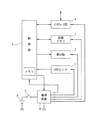
図1は、本発明の電子機器の電源装置をデジタルスチルカメラに適用した第1実施形態のブロック図である。
この電子機器であるデジタルスチルカメラは、図1に示すように、画像を撮影するCCDセンサ(カメラ部)1と、そのCCDセンサ1で撮影した画像を表示する液晶表示器のような表示部2と、そのCCDセンサ1で撮影した画像のデータを格納する画像メモリ3と、外部との間でデータの授受を行うインタフェース部4と、各部を予め定めた手順で制御する制御部5と、各部に所望の電力を供給する電源装置6とを、少なくとも備えている。電源装置6は、電源スイッチ7を介して電池8に接続されている。
【0013】
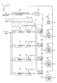
次に、第1実施形態に係る電源装置6の具体的な構成について、図2を参照して説明する。
この第1実施形態に係る電源装置6は、図2に示すように、制御回路5に電力を供給する電源回路31と、CCDセンサ1に電力を供給する電源回路32と、表示部2に電力を供給する電源回路33と、画像メモリ3に電力を供給する電源回路34と、インタフェース部4に電力を供給する電源回路35とを備え、ラッチ回路12〜15に格納される電源回路32〜35の起動順序またはその起動タイミングを制御するための各起動制御データに基づいて、電源回路32〜35が起動制御されるようになっている。
【0014】
すなわち、電源装置6は、図2に示すように、シフトレジスタ11と、ラッチ回路12〜15と、ゲート回路16〜19と、クロック発生回路20と、カウンタ21と、一致回路22〜25と、電源回路31〜35とを備えている。
シフトレジスタ11は、上記のようにラッチ回路12〜15に格納する電源回路32〜35の起動制御データと、ラッチ回路12〜15に割り当てられているアドレスを示すアドレスデータとからなるデータを、一時的に記憶するレジスタである。シフトレジスタ11は、上記のデータを入力するデータ入力端子と、クロックを入力するクロック入力端子とを備えている。
【0015】
ここで、シフトレジスタ11に格納されるデータは例えば8ビットからなり、その8ビットのうち上位側の3ビットが上記のアドレスデータとして割り当てられ、そのうちの下位側の5ビットが上記の起動データとして割り当てられるものとする。
ゲート回路16〜19は、シフトレジスタ11に格納される8ビットのデータのうち上位側の3ビットのアドレスデータを受け取ると、そのアドレスデータで指定されるラッチ回路12〜15に、データの書き込みを許可するストローブ信号を供給する回路である。
【0016】
ラッチ回路12〜15は、各電源回路32〜35の起動制御データを格納する記憶回路である。この各ラッチ回路12〜15は、シフトレジスタ11に格納される8ビットのデータのうち上位側の3ビットのアドレスデータに基づいてゲート回路16〜19からストローブ信号が供給される場合に、そのシフトレジスタ11に格納される8ビットのデータのうち下位側の5ビットの起動制御データが格納されるようになっている。
【0017】
クロック発生回路20は、制御回路5からのクロック発生信号に基づいて所定周期のクロックパルスを発生する回路である。このクロック発生回路20で発生されるクロックパルスは、カウンタ21に供給されるようになっている。
ここで、クロック発生回路20は、発生するクロックパルスの周期を任意に設定できるようにしても良い。
【0018】
カウンタ21は、クロック発生回路20からのクロックパスルを計数するものであり、その計数値(カウント値)は一致回路22〜25にそれぞれ供給されるようになっている。
一致回路22〜25は、ラッチ回路12〜15に格納される電源回路32〜35の各起動制御データ(起動数値データ)とカウンタ20の計数値とを比較し、その両者が一致したときに、電源回路32〜35を起動させる起動信号S1〜S4をそれぞれ出力する回路である。その起動信号S1〜S4は、対応する電源回路32〜34に供給されるようになっている。
【0019】
電源回路31は、電源スイッチ7の投入に基づいて起動するようになっている。電源回路32〜35は、一致回路21〜24からの起動信号S1〜S4に基づいて起動を開始し、あらかじめ決められている各出力電圧を出力するようになっている。電源回路31〜35は、その負荷の特性に応じてスイッチングレギュレータ、DC−DCコンバータ、シリーズレギュレータなどからなる。
【0020】
次に、このような構成からなる第1実施形態の動作について、図1および図2を参照して説明する。
いま、電源スイッチ7が投入(オン)されると、電源回路31が起動されて図1に示す制御部5が動作状態となり、制御部5は予め定めた手順により以下のような制御処理を行う。
【0021】
まず、シフトレジスタ11には、電源回路32の起動順序とその起動のタイミングを制御するための起動制御データ(起動数値データ)をラッチ回路12に格納するために、例えば8ビットからなるデータが制御部5から転送されて格納される。
例えば、このシフトレジスタ11には、データ「00000001」が格納される。ここで、その上位側の「000」はラッチ回路12のアドレスデータであり、その下位側の「00001」は電源回路32の起動数値データである。
【0022】
このようなデータがシフトレジスタ11に格納されると、ゲート回路16は、シフトレジスタ11に格納される上位側の3ビットのアドレスデータ「000」で指定されるラッチ回路12に対し、ストローブ信号を供給する。ラッチ回路12は、そのストローブ信号が供給されると、シフトレジスタ11に格納される下位側の5ビットの起動数値データ「00001」を格納する。
【0023】
次に、シフトレジスタ11には、例えばデータ「00100011」が格納され、その上位側の「001」はラッチ回路13のアドレスデータであり、その下位側の「00011」は電源回路33の起動数値データである。そして、その起動数値データ「00011」が、ラッチ回路13に格納される。
次に、シフトレジスタ11には、例えばデータ「01000111」が格納され、その上位側の「010」はラッチ回路14のアドレスデータであり、下位側の「00111」は電源回路34の起動数値データである。そして、その起動数値データ「00111」が、ラッチ回路14に格納される。
【0024】
最後に、シフトレジスタ11には、例えばデータ「01101111」が格納され、その上位側の「011」はラッチ回路15のアドレスデータであり、その下位側の「01111」は電源回路35の起動数値データである。そして、その起動数値データ「00111」が、ラッチ回路15に格納される。
この結果、ラッチ回路12〜15には、電源回路32〜35の起動数値データとして「00001」、「00011」、「00111」、「01111」がそれぞれ格納されることになる。
【0025】
次に、図1の制御部5からクロック発生回路20に対してクロック発生信号が供給されると、クロック発生回路20が所定のクロックパルスを発生し、この発生したクロックパルスがカウンタ21に供給される。カウンタ21はそのパルスを計数し、その計数値が一致回路22〜25にそれぞれ供給される。
一致回路22は、カウンタ21からの計数値「00001」とラッチ回路12に格納される起動数値データ「00001」とが一致すると、起動信号S1を電源回路32に供給する。電源回路32は、その起動信号S1に基づいて起動を開始し、あらかじめ決められている出力電圧を図1に示すCCDセンサ1に対して供給する。
【0026】
また、一致回路23は、カウンタ21からの計数値「00011」とラッチ回路13に格納される起動数値データ「00011」とが一致すると、起動信号S2を電源回路33に供給する。電源回路33は、その起動信号S2に基づいて起動を開始し、あらかじめ決められている出力電圧を図1に示す表示部2に対して供給する。
【0027】
さらに、一致回路24は、カウンタ21からの計数値「00111」とラッチ回路14に格納される起動数値データ「00111」とが一致すると、起動信号S3を電源回路34に供給する。電源回路34は、その起動信号S3に基づいて起動を開始し、あらかじめ決められている出力電圧を図1に示す画像メモリ3に対して供給する。
【0028】
また、一致回路25は、カウンタ21からの計数値「01111」とラッチ回路15に格納される起動数値データ「01111」とが一致すると、起動信号S4を電源回路35に供給する。電源回路35は、その起動信号S4に基づいて起動を開始し、あらかじめ決められている出力電圧を図1に示すインタフェース部4に対して供給する。
【0029】
以上説明したように、この第1実施形態によれば、複数の電源回路32〜35を同時に起動しないので、突入電流を低減できる。
また、第1実施形態によれば、電源回路32〜35の起動順序や起動タイミングを制御する起動制御データを、デジタルスチルカメラなどの電子機器の都合、またはその電子機器の各構成要素(各デバイス)の特性などに応じてあらかじめ設定しておき、その設定に応じて電源回路32〜35の起動制御ができる。
【0030】
次に、第2実施形態の構成について説明する。
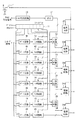
この第2実施形態は、第1実施形態と同様にデジタルスチルカメラに適用したものであり、図1および図2に示す電源装置6を、図3に示す電源装置に置き換えたものである。
すなわち、この第2実施形態に係る電源装置は、図3に示すように、制御回路5に電力を供給する電源回路31と、CCDセンサ1に電力を供給する電源回路32Aと、表示部2に電力を供給する電源回路33Aと、画像メモリ3に電力を供給する電源回路34Aと、インタフェース部4に電力を供給する電源回路35Aと、電源回路32A〜35Aの起動順序とその起動タイミングを制御するための各起動制御データ(起動数値データ)を格納するラッチ回路12〜15と、電源回路32A〜35Aの出力電圧を制御するための各出力電圧制御データを格納するラッチ回路42〜45と、を備えている。
【0031】
そして、この第2実施形態では、ラッチ回路12〜15に格納される各起動制御データに基づいて電源回路32A〜35Aが起動制御されるとともに、ラッチ回路42〜45に格納される各出力電圧制御データに基づいて電源回路32A〜35Aの各出力電圧が制御されるようにした。
このために、第2実施形態に係る電源装置は、図3に示すように、シフトレジスタ11と、ラッチ回路12〜15と、ラッチ回路42〜45と、ゲート回路16〜19と、ゲート回路46〜49と、クロック発生回路20と、カウンタ21と、一致回路22〜25と、電源回路31と、電源回路32A〜35Aとを備えている。
【0032】
なお、図3の電源装置は、図2の電源装置と共通部分を有するので、その共通部分の構成要素には同一符号を付してその構成要素の説明は省略する。
ゲート回路46〜49は、シフトレジスタ11に格納される8ビットのデータのうち上位側の3ビットのアドレスデータを受け取ると、そのアドレスデータで指定されるラッチ回路42〜45に、データの書き込みを許可するストローブ信号を供給する回路である。
【0033】
ラッチ回路42〜45は、各電源回路32A〜35Aの出力電圧制御データを格納する記憶回路である。この各ラッチ回路42〜45は、シフトレジスタ11に格納される8ビットのデータのうち上位側の3ビットのアドレスデータに基づいてゲート回路46〜49からストローブ信号が供給される場合に、そのフトレジスタ11に格納される8ビットのデータのうち下位側の5ビットの出力電圧制御データが格納されるようになっている。
【0034】
電源回路32A〜35Aは、一致回路22〜25からの起動信号S1〜S4に基づいて起動を開始するとともに、ラッチ回路42〜45に格納される各出力電圧制御データに基づいてその各出力電圧が制御されるようになっている。
次に、このような構成からなる第2実施形態の動作について、図1および図3を参照して説明する。
【0035】
いま、電源スイッチ7が投入されると、電源回路31が起動されて図1に示す制御部5が動作状態となり、制御部5は予め定めた手順により以下のような制御処理を行う。
まず、シフトレジスタ11には、電源回路32Aの起動順序とその起動のタイミングを示す起動数値データをラッチ回路12に格納するために、例えばデータ「00000001」が制御部5から転送されて格納される。
【0036】
このようなデータがシフトレジスタ11に格納されると、ゲート回路16は、シフトレジスタ11に格納される上位側の3ビットのアドレスデータ「000」で指定されるラッチ回路12に対し、ストローブ信号を供給する。ラッチ回路12は、そのストローブ信号が供給されると、シフトレジスタ11に格納される下位側の5ビットの起動数値データ「00001」を格納する。
【0037】
次に、シフトレジスタ11には、電源回路32Aの出力電圧制御データをラッチ回路42に格納するために、例えばデータ「00100011」が制御部5から転送されて格納される。ここで、そのデータのうち上位側の「001」はラッチ回路42のアドレスデータであり、そのデータの下位側の「00011」は電源回路32Aの出力電圧制御データである。
【0038】
このようなデータがシフトレジスタ11に格納されると、ゲート回路46は、シフトレジスタ11に格納される上位側の3ビットのアドレスデータ「001」で指定されるラッチ回路42に対し、ストローブ信号を供給する。ラッチ回路42は、そのストローブ信号が供給されると、シフトレジスタ11に格納される下位側の5ビットの出力電圧制御データ「00011」を格納する。
【0039】
次に、シフトレジスタ11には、例えばデータ「01000011」が格納され、その上位側の「010」はラッチ回路13のアドレスデータであり、下位側の「00011」は電源回路33Aの起動数値データである。そして、その起動数値データ「00011」が、ラッチ回路13に格納される。
次に、シフトレジスタ11には、例えばデータ「01100111」が格納され、上位側の「011」はラッチ回路43のアドレスデータであり、下位側の「00111」は電源回路33Aの出力電圧制御データである。そして、その出力電圧制御データ「00111」が、ラッチ回路43に格納される。
【0040】
このようにして、ラッチ回路12〜15には、電源回路32A〜35Aの起動数値データとして、例えば「00001」、「00011」、「00111」、「01111」がそれぞれ格納される。また、ラッチ回路42〜45には、電源回路32A〜35Aの出力電圧制御データとして、例えば「00011」、「00111」、「00011」、「00111」がそれぞれ格納される。
【0041】
次に、図1の制御部5からクロック発生回路20に対してクロック発生信号が供給されると、クロック発生回路20が所定のクロックパルスを発生し、この発生したクロックパルスがカウンタ21に供給される。カウンタ21はそのクロックパルスを計数し、その計数値が一致回路22〜25にそれぞれ供給される。
一致回路22は、カウンタ21からの計数値「00001」とラッチ回路12に格納される起動数値データ「00001」とが一致すると、起動信号S1を電源回路32Aに供給する。電源回路32Aは、その起動信号S1に基づいて起動を開始するとともに、ラッチ回路42に格納される出力電圧制御データ「00011」に基づいてその出力電圧を制御する。そして、その出力電圧はCCDセンサ1に対して供給される。
【0042】
また、一致回路23は、カウンタ21からの計数値「00011」とラッチ回路13に格納される起動数値データ「00011」とが一致すると、起動信号S2を電源回路33Aに供給する。電源回路33Aは、その起動信号S2に基づいて起動を開始するとともに、ラッチ回路43に格納される出力電圧制御データ「00111」に基づいてその出力電圧を制御する。そして、その出力電圧は表示部2に対して供給される。
【0043】
さらに、一致回路24は、カウンタ21からの計数値「00111」とラッチ回路14に格納される起動数値データ「00111」とが一致すると、起動信号S3を電源回路34Aに供給する。電源回路34Aは、その起動信号S3に基づいて起動を開始するとともに、ラッチ回路44に格納される出力電圧制御データ「00111」に基づいてその出力電圧を制御する。そして、その出力電圧は画像メモリ3に対して供給される。
【0044】
また、一致回路25は、カウンタ21からの計数値「01111」とラッチ回路15に格納される起動数値データ「01111」とが一致すると、起動信号S4を電源回路35Aに供給する。電源回路35Aは、その起動信号S4に基づいて起動を開始するとともに、ラッチ回路45に格納される出力電圧制御データ「00111」に基づいてその出力電圧を制御する。そして、その出力電圧はインタフェース部4に対して供給する。
【0045】
以上説明したように、この第2実施形態によれば、電源回路32A〜35Aの起動順序や起動タイミングを制御するための起動制御データとその出力電圧を制御するための出力電圧制御データとを、デジタルスチルカメラなどの電子機器の都合、またはその電子機器の各構成要素(各デバイス)の特性などに応じてそれぞれ設定しておき、その設定に応じて電源回路32A〜35Aの起動制御や出力電圧ができる。
【0046】
次に、第3実施形態の構成について説明する。
この第3実施形態は、第1実施形態と同様にデジタルスチルカメラに適用したものであり、図1および図2に示す電源装置6を、図4に示す電源装置に置き換えたものである。
すなわち、この第3実施形態に係る電源装置は、ラッチ回路12〜15に電源回路32B〜35Bの起動/停止の順序とその起動/停止のタイミングを制御するための各起動/停止制御データを格納するようにし、そのラッチ回路12〜15に格納される各起動/停止制御データに基づいて電源回路32B〜35Bを起動制御および停止制御させるようにしたものである。
【0047】
このために、第3実施形態に係る電源装置は、図4に示すように、シフトレジスタ11と、ラッチ回路12〜15と、ゲート回路16〜19と、クロック発生回路20と、アップダウンカウンタ50と、一致回路22〜25と、切換スイッチ51〜55と、電源回路31と、電源回路32B〜35Bとを備えている。
なお、図4の電源装置は、図2の電源装置と共通部分を有するので、その共通部分の構成要素には同一符号を付してその構成要素の説明は省略する。
【0048】
ラッチ回路12〜15は、各電源回路32B〜35Bの起動/停止制御データ(起動/停止数値データ)を格納する記憶回路である。このラッチ回路12〜15は、シフトレジスタ11に格納される8ビットのデータのうち上位側の3ビットのアドレスデータに基づいてゲート回路16〜19からストローブ信号が供給される場合に、そのシフトレジスタ11に格納される8ビットのデータのうち下位側の5ビットの起動/停止数値データが格納されるようになっている。
【0049】
アップダウンカウンタ50は、クロック発生回路20の発生するクロックパルスのアップカウント動作とダウンカウント動作とを行うことができるカウンタである。
スイッチ51は、図1に示す制御回路5からのスイッチ切換信号に基づき、クロック発生回路20からのクロックパルスを、アップダウンカウンタ50のアップカウント動作の入力端子側とダウンカウンタ動作の入力端子側とに振り分けるものである。
【0050】
スイッチ52〜54は、制御回路5からのスイッチ切換信号に基づき、一致回路22〜25から出力される起動信号と停止信号とを選択し、この選択した起動信号と停止信号とを電源回路32B〜35Bの起動信号入力端子と停止信号入力端子とに入力するためのものである。
電源回路32B〜35Bは、一致回路22〜25からの起動信号に基づいて起動を開始するとともに、一致回路22〜25からの停止信号に基づいて動作を停止するようになっている。
【0051】
また、電源回路32B〜35Bは、図1に示すCCDセンサ1、表示部2、画像メモリ3、およびインタフェース部4にそれぞれ電力を供給するようになっている。
次に、このような構成からなる第3実施形態の動作について、図1および図4を参照して説明する。
【0052】
いま、電源スイッチ7が投入されると、電源回路31が起動されて図1に示す制御部5が動作状態となり、制御部5は予め定めた手順により以下のような制御処理を行う。
まず、シフトレジスタ11には、電源回路32Bの起動/停止の順序とその起動/停止のタイミングを示す起動/停止数値データを格納するために、例えばデータ「00000001」が制御部5から転送されて格納される。
【0053】
ここで、そのデータのうち上位側の3ビットの「000」がラッチ回路12のアドレスを示すアドレスデータ、その下位側の5ビットの「00001」が起動/停止数値データである。
このようなデータがシフトレジスタ11に格納されると、ゲート回路16は、シフトレジスタ11に格納される上位側の3ビットのアドレスデータ「000」で指定されるラッチ回路12に対し、ストローブ信号を供給する。ラッチ回路12は、そのストローブ信号が供給されると、シフトレジスタ11に格納される下位側の5ビットの起動/停止数値データ「00001」を格納する。
【0054】
次に、シフトレジスタ11には、例えばデータ「00100011」が格納され、上位側の「001」はラッチ回路13のアドレスデータであり、下位側の「00011」は電源回路33Bの起動/停止数値データである。そして、その起動/停止数値データ「00011」は、ラッチ回路13に格納される。
次に、シフトレジスタ11には、例えばデータ「01000111」が格納され、上位側の「010」はラッチ回路14のアドレスデータであり、下位側の「00111」は電源回路34Bの起動/停止数値データである。そして、その起動/停止数値データ「00111」が、ラッチ回路14に格納される。
【0055】
最後に、シフトレジスタ11には、例えばデータ「01101111」が格納され、上位側の「011」はラッチ回路15のアドレスデータであり、下位側の「01111」は電源回路35Bの起動/停止数値データである。そして、その起動/停止数値データ「00111」が、ラッチ回路15に格納される。
この結果、ラッチ回路12〜15には、電源回路32B〜35Bの起動/停止数値データとして、例えば「00001」、「00011」、「00111」、「01111」がそれぞれ格納されることになる。
【0056】
次に、電源回路32B〜35Bを起動させる場合の各部の動作について説明する。
ここで、この動作のときには、切換スイッチ51〜55の各接点は、図示の位置にある。
この場合には、図1の制御部5からのクロック発生回路20に対してクロック発生信号が供給され、クロック発生回路20が所定のクロックパルスを発生する。このときには、その発生したクロックパルスはアップダウンカウンタ50のアップカウント動作側に供給される。この結果、カウンタ50はそのクロックパルスのアップカウント動作を開始し、その計数値が一致回路22〜25にそれぞれ供給される。
【0057】
一致回路22は、カウンタ50からの計数値「00001」とラッチ回路12に格納される起動/停止数値データ「00001」とが一致すると、起動信号を電源回路32Bの起動信号入力端子に供給する。電源回路32Bは、その起動信号に基づいて起動を開始し、あらかじめ決められている出力電圧を図1に示すCCDセンサ1に対して供給する。
【0058】
次に、一致回路23は、カウンタ50からの計数値「00011」とラッチ回路13に格納される起動/停止数値データ「00011」とが一致すると、起動信号S2を電源回路33Bの起動信号入力端子に供給する。電源回路33Bは、その起動信号に基づいて起動を開始し、あらかじめ決められている出力電圧を表示部2に対して供給する。
【0059】
次に、一致回路24は、カウンタ50からの計数値「00111」とラッチ回路14に格納される起動/停止数値データ「00111」とが一致すると、起動信号を電源回路34Bの起動信号入力端子に供給する。電源回路34Bは、その起動信号に基づいて起動を開始し、あらかじめ決められている出力電圧を図1に示す画像メモリ3に対して供給する。
【0060】
最後に、一致回路25は、カウンタ50からの計数値「01111」とラッチ回路15に格納される起動/停止数値データ「01111」とが一致すると、起動信号を電源回路35Bの起動信号入力端子に供給する。電源回路35Bは、その起動信号に基づいて起動を開始し、あらかじめ決められている出力電圧をインタフェース部4に対して供給する。
【0061】
次に、電源回路32B〜35Bの動作を停止させる場合の各部の動作について説明する。
この場合には、図1の制御回路5からのスイッチ切換信号に基づき、切換スイッチ51〜55の各接点が図示の位置から反対の位置に切り換えられる。その後、制御部5からのクロック発生回路20に対してクロック発生信号が供給され、クロック発生回路20が所定のクロックパルスを発生する。
【0062】
このとき、切換スイッチ51の切り換え接点は図示の位置とは反対の位置にあるので、その発生したパルスはアップダウンカウンタ50のダウンカウント動作側に供給される。この結果、アップダウンカウンタ50は、そのクロックパルスのダウンカウント動作を開始し、その計数値が一致回路22〜25にそれぞれ供給される。
【0063】
一致回路25は、カウンタ50からの計数値「01111」とラッチ回路15に格納される起動/停止数値データ「01111」とが一致すると、停止信号を電源回路35Bの停止信号入力端子に供給する。電源回路35Bは、その停止信号に基づいて動作を停止するので、その出力電圧のインタフェース部4に対する供給が停止される。
【0064】
また、一致回路24は、カウンタ50からの計数値「00111」とラッチ回路14に格納される起動/停止数値データ「00111」とが一致すると、停止信号を電源回路34Bの停止信号入力端子に供給する。電源回路34Bは、その停止信号に基づいて動作を停止するので、その出力電圧の画像メモリ3に対する供給が停止される。
【0065】
さらに、一致回路23は、カウンタ50からの計数値「00011」とラッチ回路13に格納される起動/停止数値データ「00011」とが一致すると、停止信号を電源回路33Bの停止信号入力端子に供給する。電源回路33Bは、その停止信号に基づいて動作を停止するので、その出力電圧の表示部2に対する供給が停止される。
【0066】
また、一致回路22は、カウンタ50からの計数値「00001」とラッチ回路12に格納される起動/停止数値データ「00001」とが一致すると、停止信号を電源回路32Bの停止信号入力端子に供給する。電源回路32Bは、その停止信号に基づいて動作を停止するので、その出力電圧のCCDセンサ1に対する供給が停止される。
【0067】
以上説明したように、この第3実施形態によれば、電源回路32B〜35Bの起動順序や起動タイミングとその停止順序や停止タイミングを制御するデータを、デジタルスチルカメラなどの電子機器の都合、またはその電子機器の各構成要素の特性などに応じて予め設定しておき、その設定に応じて電源回路32B〜35Bを起動制御および停止制御させることができる。
【0068】
なお、上記の実施形態では、ラッチ回路12〜15などに電源回路32〜35の起動制御データなどを電源の投入時に設定し、その設定した起動制御データに基づいて電源回路32〜35の起動制御などを行うようにした。
しかし、これに代えて、電源装置の出荷時に、電源回路32〜35の起動制御データなどをROM等の不揮発性メモリにあらかじめ書き込んでおき、電源投入時に、その起動制御データを読み出して電源回路32〜35の起動制御を行うようにしても良い。
【0069】
【発明の効果】
以上説明したように、本発明によれば、複数の電源回路の同時起動を避けることができるので、突入電流を低減できる。
また、本発明によれば、複数の電源回路の起動順序または起動タイミングを制御するためのデータを、電子機器の都合、またはその電子機器の各構成要素(各デバイス)の特性などに応じてあらかじめ設定しておき、その設定に応じて複数の電源回路を起動制御することができる。
【図面の簡単な説明】
【図1】本発明の第1実施形態をデジタルスチルカメラに適用した場合の構成例を示すブロック図である。
【図2】第1実施形態に係る電源装置の構成を示すブロック図である。
【図3】第2実施形態に係る電源装置の構成を示すブロック図である。
【図4】第3実施形態に係る電源装置の構成を示すブロック図である。
【符号の説明】
1はCCDセンサ、2は表示部、3は画像メモリ、4はインタフェース部、5は制御部、6は電源装置、7は電源スイッチ、11はシフトレジスタ、12〜15はラッチ回路、16〜19はゲート回路、21はカウンタ、22〜25は一致回路、31〜35は電源回路、50はアップダウンカウンタである。[0001]
TECHNICAL FIELD OF THE INVENTION
The present invention relates to a power supply device for an electronic device that supplies power to an electronic device (electronic system) such as a digital still camera.
[0002]
[Prior art]
For example, a digital still camera includes a CCD sensor that captures an image, an image memory that stores data of the image captured by the CCD sensor, a display unit that displays an image captured by the CCD sensor, and exchanges data with the outside. It is composed of an interface unit for performing, a control unit for controlling each unit, and the like.
[0003]
As a power supply device for an electronic device such as a digital still camera having such a configuration, a power supply device having a plurality of power supply circuits for supplying power to respective components of the digital still camera is known. The plurality of power supply circuits include a switching regulator, a DC-DC converter, a series regulator, and the like.
Further, in such a conventional power supply device for an electronic device, a plurality of power supply circuits are simultaneously activated when a power switch is turned on.
[0004]
[Problems to be solved by the invention]
When a plurality of power supply circuits are started at the same time, an inrush current increases at the time of starting. For this reason, when the power supply circuit is operated by a battery, the power supply voltage may temporarily drop, and the components may malfunction such as malfunction. Further, there is a possibility that a device to which power is supplied may be destroyed.
[0005]
On the other hand, each component (each device) has its own characteristic. For this reason, it is desired that the start-up order and the start-up timing of the plurality of power supply circuits be changed according to the characteristics of the respective components at the time of start-up.
SUMMARY OF THE INVENTION It is an object of the present invention to provide a power supply device for an electronic device that can reduce an inrush current and can appropriately control a start order and a start timing of a plurality of power supply circuits.
[0006]
[Means for Solving the Problems]
In order to solve the above problems and achieve the object of the present invention, each invention is configured as follows.
That is, a first invention is a power supply device for supplying power to an electronic device including a plurality of components, comprising: a plurality of power supply circuits for respectively supplying power to the plurality of components; and a plurality of power supply circuits. A storage circuit for storing start-up control data for start-up control, wherein the plurality of power supply circuits are controlled to start upon start-up based on start-up control data stored in the storage circuit. I have.
[0007]
According to a second invention, in the power supply device according to the first invention, the storage circuit further stores stop control data for stop control of the plurality of power circuits, and the plurality of power circuits are configured to stop. At this time, stop control is performed based on stop control data stored in the storage circuit.
A third invention is the power supply device according to the first or second invention, wherein the storage circuit further stores output voltage control data for controlling output voltages of the plurality of power supply circuits, In the power supply circuit, the output voltage is controlled based on a plurality of output voltage control data stored in the storage circuit.
[0008]
According to a fourth aspect, in the power supply device according to the first, second, or third aspect, the start control data comprises data for controlling a start order or a start timing of the plurality of power supply circuits, The data includes data for controlling the stop order or stop timing of the plurality of power supply circuits.
A fifth invention is a power supply device for supplying power to an electronic device including a plurality of components, wherein a plurality of power supply circuits for supplying power to the plurality of components, respectively, and activation control of the plurality of power supply circuits is provided. A plurality of first latch circuits each storing respective numerical data for performing the operation, a counter counting a predetermined clock, and comparing each numerical data stored in the plurality of first latch circuits with the count value of the counter. A plurality of matching circuits that output a start signal when the two match with each other, wherein the plurality of power supply circuits perform start-up control based on corresponding start signals from the plurality of match circuits when starting. It is supposed to be.
[0009]
A sixth invention is a power supply device for supplying power to an electronic device including a plurality of components, wherein the plurality of power supply circuits respectively supply power to the plurality of components, and a start control of the plurality of power supply circuits. And a plurality of first latch circuits respectively storing numerical data for performing stop control, an up-down counter for performing up-counting operation or down-counting operation of a predetermined clock, and when the up-down counter is up-counted Comparing each of the numerical data stored in the plurality of first latch circuits with the count value at that time, and outputting a start signal when the two coincide with each other; Then, each numerical data stored in the plurality of first latch circuits is compared with a count value at that time, and the two coincide. A plurality of sequence signal generation circuits that output a stop signal when the power supply circuit is activated, wherein the plurality of power supply circuits are controlled to be activated at the time of activation based on corresponding activation signals from the plurality of sequence signal generation circuits. In addition, at the time of stop, stop control is performed based on corresponding stop signals from the plurality of sequence signal generation circuits.
[0010]
A seventh invention is the power supply device according to the fifth or sixth invention, further comprising a plurality of second latch circuits storing output voltage control data for controlling each output voltage of the plurality of power supply circuits, The output voltages of the plurality of power supply circuits are controlled based on the respective output voltage control data stored in the plurality of second latch circuits.
[0011]
According to the present invention having such a configuration, simultaneous activation of a plurality of power supply circuits can be avoided, so that inrush current can be reduced.
Further, in the present invention, data for controlling the activation sequence or the activation timing of the plurality of power supply circuits is preset in accordance with the convenience of the electronic device or the characteristics of each component (each device) of the electronic device. In advance, a plurality of power supply circuits can be controlled to start according to the setting.
[0012]
BEST MODE FOR CARRYING OUT THE INVENTION
Hereinafter, embodiments of the present invention will be described.
FIG. 1 is a block diagram of a first embodiment in which a power supply device of an electronic apparatus of the present invention is applied to a digital still camera.
As shown in FIG. 1, a digital still camera as an electronic apparatus includes a CCD sensor (camera unit) 1 for photographing an image and a
[0013]
Next, a specific configuration of the
As shown in FIG. 2, the
[0014]
That is, as shown in FIG. 2, the
The
[0015]
Here, the data stored in the
When the
[0016]
The
[0017]
The
Here, the
[0018]
The counter 21 counts a clock pulse from the
The
[0019]
The
[0020]
Next, the operation of the first embodiment having such a configuration will be described with reference to FIGS.
When the
[0021]
First, in order to store start control data (start numerical data) for controlling the start sequence and the start timing of the
For example, the
[0022]
When such data is stored in the
[0023]
Next, for example, data “00100011” is stored in the
Next, for example, data “01000111” is stored in the
[0024]
Finally, the
As a result, "00001", "00011", "00111", and "01111" are stored in the
[0025]
Next, when a clock generation signal is supplied from the control unit 5 of FIG. 1 to the
When the count value “00001” from the counter 21 matches the activation numerical data “00001” stored in the
[0026]
When the count value “00011” from the counter 21 matches the start numerical data “00011” stored in the
[0027]
Further, when the count value “00111” from the counter 21 matches the activation numerical data “00111” stored in the
[0028]
Further, when the count value “01111” from the counter 21 matches the start numerical data “01111” stored in the
[0029]
As described above, according to the first embodiment, since the plurality of
Further, according to the first embodiment, the start control data for controlling the start sequence and the start timing of the
[0030]
Next, the configuration of the second embodiment will be described.
The second embodiment is applied to a digital still camera, similarly to the first embodiment, and the
That is, as shown in FIG. 3, the power supply device according to the second embodiment includes a
[0031]
In the second embodiment, the
For this purpose, as shown in FIG. 3, the power supply device according to the second embodiment includes a
[0032]
Since the power supply device of FIG. 3 has a common part with the power supply device of FIG. 2, the components of the common portion are denoted by the same reference numerals and the description of the components is omitted.
When the
[0033]
The
[0034]
The
Next, the operation of the second embodiment having such a configuration will be described with reference to FIGS.
[0035]
Now, when the
First, for example, data “00000001” is transferred from the control unit 5 and stored in the
[0036]
When such data is stored in the
[0037]
Next, in order to store the output voltage control data of the
[0038]
When such data is stored in the
[0039]
Next, for example, data “01000011” is stored in the
Next, for example, data “01100111” is stored in the
[0040]
In this way, in the
[0041]
Next, when a clock generation signal is supplied from the control unit 5 of FIG. 1 to the
When the count value “00001” from the counter 21 matches the activation numerical data “00001” stored in the
[0042]
Further, when the count value “00011” from the counter 21 matches the activation numerical data “00011” stored in the
[0043]
Furthermore, when the count value “00111” from the counter 21 matches the activation numerical data “00111” stored in the
[0044]
Further, when the count value “01111” from the counter 21 matches the activation numerical data “01111” stored in the
[0045]
As described above, according to the second embodiment, the start control data for controlling the start order and the start timing of the
[0046]
Next, the configuration of the third embodiment will be described.
The third embodiment is applied to a digital still camera, similarly to the first embodiment, and the
That is, in the power supply device according to the third embodiment, the start / stop control data for controlling the start / stop sequence and the start / stop timing of the power circuits 32B to 35B are stored in the
[0047]
For this purpose, as shown in FIG. 4, the power supply device according to the third embodiment includes a
Note that the power supply device of FIG. 4 has a common part with the power supply device of FIG.
[0048]
The
[0049]
The up / down
The
[0050]
The
The power supply circuits 32B to 35B start up based on start signals from the matching
[0051]
The power supply circuits 32B to 35B supply power to the
Next, the operation of the third embodiment having such a configuration will be described with reference to FIGS.
[0052]
Now, when the
First, for example, data “00000001” is transferred from the control unit 5 to the
[0053]
Here, the upper three bits “000” of the data are address data indicating the address of the
When such data is stored in the
[0054]
Next, for example, data “00100011” is stored in the
Next, for example, data “01000111” is stored in the
[0055]
Lastly, the
As a result, for example, “00001”, “00011”, “00111”, and “01111” are stored in the
[0056]
Next, the operation of each unit when activating the power supply circuits 32B to 35B will be described.
Here, at the time of this operation, the contacts of the changeover switches 51 to 55 are at the positions shown in the figure.
In this case, a clock generation signal is supplied from the control unit 5 of FIG. 1 to the
[0057]
When the count value “00001” from the counter 50 matches the start / stop numerical data “00001” stored in the
[0058]
Next, when the count value “00011” from the counter 50 matches the start / stop numerical data “00011” stored in the
[0059]
Next, when the count value “00111” from the counter 50 matches the start / stop numerical data “00111” stored in the
[0060]
Finally, when the count value “01111” from the counter 50 matches the start / stop numerical data “01111” stored in the
[0061]
Next, the operation of each unit when the operation of the power supply circuits 32B to 35B is stopped will be described.
In this case, the respective contacts of the changeover switches 51 to 55 are switched from the illustrated position to the opposite position based on the switch switching signal from the control circuit 5 in FIG. Thereafter, a clock generation signal is supplied from the control unit 5 to the
[0062]
At this time, since the changeover contact of the
[0063]
When the count value “01111” from the counter 50 matches the start / stop numerical data “01111” stored in the
[0064]
When the count value “00111” from the counter 50 matches the start / stop numerical data “00111” stored in the
[0065]
Further, when the count value “00011” from the counter 50 matches the start / stop numerical data “00011” stored in the
[0066]
When the count value “00001” from the counter 50 matches the start / stop numerical data “00001” stored in the
[0067]
As described above, according to the third embodiment, data for controlling the start order and start timing of the
[0068]
In the above embodiment, the activation control data and the like for the
However, instead of this, at the time of shipment of the power supply device, start-up control data and the like of the
[0069]
【The invention's effect】
As described above, according to the present invention, simultaneous activation of a plurality of power supply circuits can be avoided, so that inrush current can be reduced.
Further, according to the present invention, data for controlling the activation sequence or the activation timing of the plurality of power supply circuits is stored in advance in accordance with the convenience of the electronic device or the characteristics of each component (each device) of the electronic device. After setting, a plurality of power supply circuits can be controlled to start according to the setting.
[Brief description of the drawings]
FIG. 1 is a block diagram illustrating a configuration example when a first embodiment of the present invention is applied to a digital still camera.
FIG. 2 is a block diagram illustrating a configuration of a power supply device according to the first embodiment.
FIG. 3 is a block diagram illustrating a configuration of a power supply device according to a second embodiment.
FIG. 4 is a block diagram illustrating a configuration of a power supply device according to a third embodiment.
[Explanation of symbols]
1 is a CCD sensor, 2 is a display unit, 3 is an image memory, 4 is an interface unit, 5 is a control unit, 6 is a power supply device, 7 is a power switch, 11 is a shift register, 12 to 15 are latch circuits, and 16 to 19 Is a gate circuit, 21 is a counter, 22 to 25 are matching circuits, 31 to 35 are power supply circuits, and 50 is an up / down counter.
Claims (7)
前記複数の構成要素に電力をそれぞれ供給する複数の電源回路と、
前記複数の電源回路を起動制御するための起動制御データを格納する記憶回路とを備え、
前記複数の電源回路は、起動の際に、前記記憶回路に格納される起動制御データに基づいて起動制御されるようになっていることを特徴とする電子機器の電源装置。A power supply device for supplying power to an electronic device including a plurality of components,
A plurality of power supply circuits for respectively supplying power to the plurality of components,
A storage circuit for storing activation control data for controlling activation of the plurality of power supply circuits,
The power supply device for an electronic device, wherein the plurality of power supply circuits are controlled to be activated at the time of activation based on activation control data stored in the storage circuit.
前記複数の電源回路は、停止の際に、前記記憶回路に格納される停止制御データに基づいて停止制御されるようになっていることを特徴とする請求項1に記載の電子機器の電源装置。The storage circuit further stores stop control data for controlling stop of the plurality of power supply circuits,
2. The power supply device for an electronic device according to claim 1, wherein when the plurality of power supply circuits are stopped, stop control is performed based on stop control data stored in the storage circuit. 3. .
前記複数の電源回路は、前記記憶回路に格納される複数の出力電圧制御データに基づいて出力電圧が制御されるようになっていることを特徴とする請求項1または請求項2に記載の電子機器の電源装置。The storage circuit further stores output voltage control data for controlling each output voltage of the plurality of power supply circuits,
3. The electronic device according to claim 1, wherein an output voltage of the plurality of power supply circuits is controlled based on a plurality of output voltage control data stored in the storage circuit. Equipment power supply.
前記停止制御データは前記複数の電源回路の停止順序または停止タイミングを制御するためのデータからなることを特徴とする請求項1、請求項2、または請求項3に記載の電子機器の電源装置。The start control data includes data for controlling a start order or a start timing of the plurality of power supply circuits,
4. The power supply device for an electronic device according to claim 1, wherein the stop control data includes data for controlling a stop sequence or a stop timing of the plurality of power supply circuits. 5.
前記複数の構成要素に電力をそれぞれ供給する複数の電源回路と、
前記複数の電源回路を起動制御するための各数値データをそれぞれ格納する複数の第1ラッチ回路と、
所定のクロックを計数するカウンタと、
前記複数の第1ラッチ回路に格納される各数値データと前記カウンタの計数値とを比較し、その両者が一致するときに起動信号を出力する複数の一致回路とを備え、
前記複数の電源回路は、起動の際に、前記複数の一致回路からの対応する起動信号に基づいて起動制御されるようになっていることを特徴とする電子機器の電源装置。A power supply device for supplying power to an electronic device including a plurality of components,
A plurality of power supply circuits for respectively supplying power to the plurality of components,
A plurality of first latch circuits each storing numerical data for controlling the activation of the plurality of power supply circuits;
A counter for counting a predetermined clock;
A plurality of coincidence circuits for comparing each numerical data stored in the plurality of first latch circuits with the count value of the counter, and outputting a start signal when both coincide with each other;
The power supply device for an electronic device, wherein the plurality of power supply circuits are controlled to be activated at the time of activation based on corresponding activation signals from the plurality of matching circuits.
前記複数の構成要素に電力をそれぞれ供給する複数の電源回路と、
前記複数の電源回路を起動制御および停止制御するための各数値データをそれぞれ格納する複数の第1ラッチ回路と、
所定のクロックのアップカウント動作またはダウンカウント動作を行うアップダウンカウンタと、
前記アップダウンカウンタをアップカウント動作させたときに、前記複数の第1ラッチ回路に格納される各数値データとそのときの計数値とを比較し、その両者が一致するときに起動信号を出力し、一方、前記アップダウンカウンタをダウンカウント動作させたときに、前記複数の第1ラッチ回路に格納される各数値データとそのときの計数値とを比較し、その両者が一致するときに停止信号を出力する複数のシーケンス信号発生回路とを備え、
前記複数の電源回路は、起動の際に、前記複数のシーケンス信号発生回路からの対応する起動信号に基づいて起動制御されるとともに、停止の際に、前記複数のシーケンス信号発生回路からの対応する停止信号に基づいて停止制御されるようになっていることを特徴とする電子機器の電源装置。A power supply device for supplying power to an electronic device including a plurality of components,
A plurality of power supply circuits for respectively supplying power to the plurality of components,
A plurality of first latch circuits each storing numerical data for controlling the start and stop of the plurality of power circuits;
An up-down counter that performs an up-count operation or a down-count operation of a predetermined clock;
When the up / down counter is up-counted, each numerical data stored in the plurality of first latch circuits is compared with the count value at that time, and a start signal is output when they match. On the other hand, when the up / down counter is operated to count down, each numerical data stored in the plurality of first latch circuits is compared with the count value at that time, and when both of them match, a stop signal is output. And a plurality of sequence signal generation circuits that output
The plurality of power supply circuits are controlled at the time of activation based on corresponding activation signals from the plurality of sequence signal generation circuits, and at the time of shutdown, are controlled by the plurality of sequence signal generation circuits. A power supply device for an electronic device, wherein a stop control is performed based on a stop signal.
前記複数の電源回路は、前記複数の第2ラッチ回路に格納される各出力電圧制御データに基づいて出力電圧が制御されるようになっていることを特徴とする請求項5または請求項6に記載の電子機器の電源装置。A plurality of second latch circuits for storing output voltage control data for controlling output voltages of the plurality of power supply circuits;
7. The power supply circuit according to claim 5, wherein an output voltage of the plurality of power supply circuits is controlled based on output voltage control data stored in the plurality of second latch circuits. A power supply device for the electronic device according to the item.
Priority Applications (1)
| Application Number | Priority Date | Filing Date | Title |
|---|---|---|---|
| JP2003072566A JP3891132B2 (en) | 2003-03-17 | 2003-03-17 | Electronic equipment power supply |
Applications Claiming Priority (1)
| Application Number | Priority Date | Filing Date | Title |
|---|---|---|---|
| JP2003072566A JP3891132B2 (en) | 2003-03-17 | 2003-03-17 | Electronic equipment power supply |
Publications (2)
| Publication Number | Publication Date |
|---|---|
| JP2004282930A true JP2004282930A (en) | 2004-10-07 |
| JP3891132B2 JP3891132B2 (en) | 2007-03-14 |
Family
ID=33288731
Family Applications (1)
| Application Number | Title | Priority Date | Filing Date |
|---|---|---|---|
| JP2003072566A Expired - Fee Related JP3891132B2 (en) | 2003-03-17 | 2003-03-17 | Electronic equipment power supply |
Country Status (1)
| Country | Link |
|---|---|
| JP (1) | JP3891132B2 (en) |
Cited By (10)
| Publication number | Priority date | Publication date | Assignee | Title |
|---|---|---|---|---|
| JP2006204013A (en) * | 2005-01-20 | 2006-08-03 | Nec Corp | Apparatus, method, and program for controlling power application sequence |
| JP2007079881A (en) * | 2005-09-14 | 2007-03-29 | Nec Corp | Power source supply system, portable apparatus, and method of controlling power-on sequence used for them |
| JP2007274868A (en) * | 2006-03-31 | 2007-10-18 | Mitsubishi Electric Corp | Programmable controller activation method and programmable controller |
| JP2008148385A (en) * | 2006-12-06 | 2008-06-26 | Seiko Epson Corp | Electronic device, control method thereof, and control program thereof |
| JP2009060690A (en) * | 2007-08-30 | 2009-03-19 | Denso Corp | Power control device |
| JP2010045944A (en) * | 2008-08-18 | 2010-02-25 | Rohm Co Ltd | Power supply apparatus |
| KR100968802B1 (en) * | 2007-02-16 | 2010-07-08 | 후지쯔 세미컨덕터 가부시키가이샤 | Power circuit, power control circuit and power control method |
| JP2010170341A (en) * | 2009-01-22 | 2010-08-05 | Fujitsu Ltd | Power supply control device and power supply control system |
| KR20120085786A (en) * | 2009-09-23 | 2012-08-01 | 에스티 에릭슨 에스에이 | Power supply start-up mechanism, apparatus, and method for controlling activation of power supply circuits |
| JP2016218625A (en) * | 2015-05-18 | 2016-12-22 | 株式会社アイエイアイ | Control apparatus and control method |
-
2003
- 2003-03-17 JP JP2003072566A patent/JP3891132B2/en not_active Expired - Fee Related
Cited By (13)
| Publication number | Priority date | Publication date | Assignee | Title |
|---|---|---|---|---|
| JP2006204013A (en) * | 2005-01-20 | 2006-08-03 | Nec Corp | Apparatus, method, and program for controlling power application sequence |
| JP2007079881A (en) * | 2005-09-14 | 2007-03-29 | Nec Corp | Power source supply system, portable apparatus, and method of controlling power-on sequence used for them |
| JP2007274868A (en) * | 2006-03-31 | 2007-10-18 | Mitsubishi Electric Corp | Programmable controller activation method and programmable controller |
| JP2008148385A (en) * | 2006-12-06 | 2008-06-26 | Seiko Epson Corp | Electronic device, control method thereof, and control program thereof |
| KR100968802B1 (en) * | 2007-02-16 | 2010-07-08 | 후지쯔 세미컨덕터 가부시키가이샤 | Power circuit, power control circuit and power control method |
| US7952234B2 (en) | 2007-02-16 | 2011-05-31 | Fujitsu Semiconductor Limited | Power supply circuit, power supply control circuit and power supply control method |
| JP2009060690A (en) * | 2007-08-30 | 2009-03-19 | Denso Corp | Power control device |
| JP2010045944A (en) * | 2008-08-18 | 2010-02-25 | Rohm Co Ltd | Power supply apparatus |
| JP2010170341A (en) * | 2009-01-22 | 2010-08-05 | Fujitsu Ltd | Power supply control device and power supply control system |
| KR20120085786A (en) * | 2009-09-23 | 2012-08-01 | 에스티 에릭슨 에스에이 | Power supply start-up mechanism, apparatus, and method for controlling activation of power supply circuits |
| JP2013505506A (en) * | 2009-09-23 | 2013-02-14 | エスティー‐エリクソン、ソシエテ、アノニム | Power supply start mechanism, device and method for controlling start-up of power supply circuit |
| KR101657205B1 (en) | 2009-09-23 | 2016-09-19 | 텔레호낙티에볼라게트 엘엠 에릭슨(피유비엘) | Power supply start-up mechanism, apparatus, and method for controlling activation of power supply circuits |
| JP2016218625A (en) * | 2015-05-18 | 2016-12-22 | 株式会社アイエイアイ | Control apparatus and control method |
Also Published As
| Publication number | Publication date |
|---|---|
| JP3891132B2 (en) | 2007-03-14 |
Similar Documents
| Publication | Publication Date | Title |
|---|---|---|
| JP3891132B2 (en) | Electronic equipment power supply | |
| JP2020530748A (en) | Charging circuit, terminal, and charging method | |
| US8412965B2 (en) | PWM timer for power supply | |
| JPH1080069A (en) | Electronic still camera | |
| JP2005242665A (en) | Constant voltage circuit | |
| US7253798B2 (en) | Charge pump | |
| JP3480721B2 (en) | Power on / off sequence controller | |
| JPH0583884A (en) | D.c. power supply switching device | |
| US11190099B2 (en) | Voltage conversion device | |
| CN219916685U (en) | Power supply time sequence control circuit and display device | |
| JP2005065438A (en) | Activation control circuit for multi-output power supply device | |
| JP2002202829A (en) | Microcomputer | |
| CN108828993B (en) | Terminal startup control circuit and data acquisition terminal | |
| JP2002099332A (en) | Multi-voltage DC power supply | |
| JP2020170377A (en) | Power control circuit, power management circuit and electronic equipment | |
| JP2002136101A (en) | Display unit for setting voltage and current of power unit | |
| JP3495533B2 (en) | Microcomputer clock switching circuit | |
| JP3285208B2 (en) | Semiconductor device | |
| JP2004266953A (en) | Dc power supply unit | |
| JP7693275B2 (en) | Control device, control method, and program | |
| KR200181757Y1 (en) | Camera capable of specifying the function of a button | |
| JP2003125533A (en) | Method and apparatus for controlling feed circuit | |
| JP4821139B2 (en) | Power control method for portable device and power control circuit for portable device | |
| JP2001242518A (en) | Power supply device and camera with same | |
| JP2005326233A (en) | Electronic device having battery remaining amount detection device |
Legal Events
| Date | Code | Title | Description |
|---|---|---|---|
| A621 | Written request for application examination |
Free format text: JAPANESE INTERMEDIATE CODE: A621 Effective date: 20051026 |
|
| A977 | Report on retrieval |
Free format text: JAPANESE INTERMEDIATE CODE: A971007 Effective date: 20060727 |
|
| A131 | Notification of reasons for refusal |
Free format text: JAPANESE INTERMEDIATE CODE: A131 Effective date: 20060801 |
|
| A521 | Request for written amendment filed |
Free format text: JAPANESE INTERMEDIATE CODE: A523 Effective date: 20060929 |
|
| TRDD | Decision of grant or rejection written | ||
| A01 | Written decision to grant a patent or to grant a registration (utility model) |
Free format text: JAPANESE INTERMEDIATE CODE: A01 Effective date: 20061114 |
|
| A61 | First payment of annual fees (during grant procedure) |
Free format text: JAPANESE INTERMEDIATE CODE: A61 Effective date: 20061127 |
|
| R150 | Certificate of patent or registration of utility model |
Free format text: JAPANESE INTERMEDIATE CODE: R150 |
|
| FPAY | Renewal fee payment (event date is renewal date of database) |
Free format text: PAYMENT UNTIL: 20101215 Year of fee payment: 4 |
|
| FPAY | Renewal fee payment (event date is renewal date of database) |
Free format text: PAYMENT UNTIL: 20101215 Year of fee payment: 4 |
|
| FPAY | Renewal fee payment (event date is renewal date of database) |
Free format text: PAYMENT UNTIL: 20111215 Year of fee payment: 5 |
|
| FPAY | Renewal fee payment (event date is renewal date of database) |
Free format text: PAYMENT UNTIL: 20111215 Year of fee payment: 5 |
|
| FPAY | Renewal fee payment (event date is renewal date of database) |
Free format text: PAYMENT UNTIL: 20121215 Year of fee payment: 6 |
|
| FPAY | Renewal fee payment (event date is renewal date of database) |
Free format text: PAYMENT UNTIL: 20121215 Year of fee payment: 6 |
|
| FPAY | Renewal fee payment (event date is renewal date of database) |
Free format text: PAYMENT UNTIL: 20131215 Year of fee payment: 7 |
|
| LAPS | Cancellation because of no payment of annual fees |