【0001】
【発明の属する技術分野】
本発明は電源回路に係り、入力電圧が動作電圧範囲にない間は電圧出力を遮断するものに関する。
【0002】
【従来の技術】
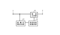
入力される直流電圧を定電圧化して出力する電源回路には、例えば、図2にブロック図で示す如きものがある。このような電源回路は、例えば、商用電源から整流された電圧や、停電時の非常用発電機や車載用のバッテリー等からの直流電圧を定電圧化するもの等に用いられ、入力端1からの入力電圧を電源主回路11でスイッチングレギュレータを用いて定電圧化し、出力端2から出力する。負荷短絡保護回路13は、電源主回路11の負荷回路に短絡が生じ出力電圧が低下した場合にこれを検出し、出力遮断信号を出力し、電源主回路11の出力を遮断する回路である。また、低電圧検出回路12は、入力電圧が供給されたとき、入力端1からの入力電圧が電源主回路11の動作電圧範囲の下限より高くなった場合にこれを検出し、負荷短絡保護回路13をリセットして電源主回路11の電圧出力を開始させる回路であるが、この低電圧検出回路12は、電源主回路11の入力電圧が動作電圧範囲の下限からさらに下降する過渡時にも負荷短絡保護回路13をリセットしてしまうために電源主回路11は動作状態が維持され、予め設定された値より低い不安定な電圧を出力し続けることになる。(例えば、特許文献1参照。)
このため、例えば、マイコンを用いた回路が負荷として接続されるような場合、負荷回路には規定より低い不安定な電圧が供給されるので正常な動作ができず、メモリデータが破壊される等の問題が生じる場合がある。
【0003】
【特許文献1】
特開2000−324678号公報(第2−3頁、図1、図2)
【0004】
【発明が解決しようとする課題】
本発明は以上述べた問題点を解決し、入力電圧が電源主回路の動作電圧範囲まで上昇すると出力短絡保護機能がリセットされ、電源主回路から安定化された電圧が出力され、入力電圧が電源主回路の動作電圧範囲より低下すると出力短絡保護機能が作動し、電源主回路の出力が遮断され、負荷に不安定な電圧が出力されず、例えば、負荷回路に接続されたメモリのデータが破壊されたり変形されないようにした電源回路を提供することを目的とする。
【0005】
【課題を解決するための手段】
本発明は上述の課題を解決するため、直流の入力電圧を定電圧化して出力する電源主回路と、同電源主回路の負荷に短絡が生じたとき、もしくは、前記入力電圧が前記電源主回路の動作電圧範囲より低いとき同電源主回路の出力を遮断する出力短絡保護回路と、前記入力電圧を検出する入力電圧検出回路と、同入力電圧検出回路で検出された電圧が所定の電圧以上に上昇したときパルス信号を出力し前記出力短絡保護回路をリセットして保護機能を解除するリセットパルス発生回路とからなり、
前記リセットパルス発生回路は、前記入力電圧が前記電源主回路の動作電圧範囲より低い値から上昇する場合、同入力電圧が所定値になったときの前記入力電圧検出回路からの信号に基づきパルス信号を発生し、前記出力短絡保護回路をリセットして前記電源主回路から電圧を出力させ、前記入力電圧が前記電源主回路の動作電圧範囲より低い範囲で下降する場合は、パルス信号を発生させないで前記出力短絡保護回路を動作させ、前記電源主回路から電圧を出力させないようにする。
【0006】
なお、前記リセットパルス発生回路は、一端を前記入力電圧検出回路の出力端に接続したコンデンサと、一端を同コンデンサの他端に、他端を接地に接続した抵抗器と、カソードを前記コンデンサの他端に、アノードを接地にそれぞれ接続したダイオードと、ベースを前記ダイオードのカソードに、エミッタを接地に、コレクタを前記出力短絡保護回路にそれぞれ接続したNPN型トランジスタとで構成する。
【0007】
【発明の実施の形態】
以下、図面に基づいて本発明による電源回路を詳細に説明する。
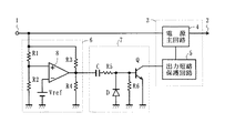
図1は本発明による電源回路の一実施例を示す要部ブロック図である。図の1は直流電圧を入力する入力端、2は安定化された電圧を出力する出力端、3は電源ICユニットで、電源ICユニット3の4は電源主回路、5は出力短絡保護回路である。6は入力電圧検出回路、7はリセットパルス発生回路で、入力電圧検出回路6のR1〜R4は抵抗器、Vrefは基準電圧、8はコンパレータで、リセットパルス発生回路7のCはコンデンサ、R5とR6は抵抗器、Dはダイオード、QはNPN型トランジスタである。
【0008】
以上の構成において、次にその動作を説明する。
入力端1には、商用電源から整流された電圧や、停電時の非常用発電機や車載用のバッテリー等からの直流電圧が入力する。入力端1からの入力電圧は電源ICユニット3の電源主回路4に入力し、スイッチングレギュレータにより定電圧化され、出力端2から負荷回路に出力される。出力短絡保護回路5は電源ICユニット3内に設けられ、入力電圧が電源主回路4の動作電圧範囲に達するまでの間は電源主回路4の電圧出力を遮断し、また、電源主回路4の出力電圧を監視し、負荷に短絡が生じた場合、出力電圧の低下に応動して出力遮断信号(Lレベル)を出力し、電源主回路4の電圧出力を遮断し、電源主回路4を破壊から保護する。
【0009】
入力電圧検出回路6は入力端1からの電圧を検出するもので、抵抗器R1とR2で入力電圧を分圧し、コンパレータ8の+端子に印加し、−端子に基準電圧Vrefを印加する。抵抗器R1とR2は、入力電圧が電源主回路4の動作電圧範囲の下限のとき、分圧値が基準電圧Vrefより僅かに高い値となるように設定する。そして、コンパレータ8で二つの電圧を比較し、入力電圧が電源主回路4の動作電圧範囲の下限より高い、すなわち+端子の電圧が−端子の電圧より高いときHレベルを出力し、低いときLレベルを出力する。抵抗器R3とR4はコンパレータ8の出力端が使用最大電圧を越えないように所定の電圧以内に抑えるための抵抗器である。
リセットパルス発生回路7はパルス信号を発生して出力短絡保護回路5をリセットし、保護機能を解除し、電源主回路4に電圧を出力させる。
【0010】
電源がオンされると、入力端1からの電圧が徐々に上昇する。入力電圧が電源主回路4の動作電圧範囲の下限より低い間、コンパレータ8の出力はLレベルで、出力端は抵抗器R3とR4で入力電圧を分圧した値に固定されるので、リセットパルス発生回路7のコンデンサCは充電されず、従ってトランジスタQはオフのままであり、コレクタはHレベルにあり、出力短絡保護回路5は入力がHレベルなので保護機能が働き、電源主回路4は電圧を出力しない。
入力電圧が動作電圧範囲の下限より高くなると、コンパレータ8の出力がHレベルに転ずる。この瞬間、リセットパルス発生回路7のコンデンサCを通じてコンパレータ8の出力の立ち上がり成分がパルス波形(微分パルス)となり、このパルスが抵抗器R5を介してトランジスタQのベースに加わり、トランジスタQがオンし、出力短絡保護回路5の入力をゼロレベルに引き下げ、保護機能を解除(リセット)し、電源主回路4からは安定化された所定の電圧が出力される。
【0011】
電源がオフされると、入力端1の電圧は急激に下降し、出力短絡保護回路5が作動して電源主回路4は電圧を出力しなくなる。入力電圧が電源主回路4の動作電圧範囲の下限より低くなると、入力電圧検出回路6のコンパレータ8の出力がLレベルに転じ、この瞬間、リセットパルス発生回路7のコンデンサCを通じてトランジスタQのベースに負の微分パルスが加わるが、このパルスはダイオードDによって吸収され、ダイオードDの順方向の電圧以上にはならないので、トランジスタQはオンされず(リセットパルスは出力されず)、出力短絡保護回路5は動作したままでリセットされず、これにより、電源主回路4から不安定な電圧が出力される状態が回避される。
【0012】
このように、電源がオフされたとき、入力電圧が下降する過渡時に電源主回路4から不安定な電圧が出力されないので、例えば、負荷にメモリを用いた回路が接続されているような場合に不安定な電圧による回路の異常動作でメモリデータが消滅あるいは変形するといった事態を避けることができる。
【0013】
【発明の効果】
以上に説明したように、本発明による電源回路によれば、電源がオンされたとき、入力電圧がどのように上昇しても、予め設定された電圧(電源主回路の動作電圧範囲の下限)まで上昇すると出力短絡保護回路がリセットされ、電源主回路から定電圧化された電圧が出力開始され、負荷に短絡が生じると電源主回路の保護のため電圧出力が遮断される。また、電源がオフされ、入力電圧が電源主回路の動作電圧範囲より低くなると、出力短絡保護回路が作動し、電源主回路の電圧出力が遮断される。これにより、例えば、負荷にメモリを用いた回路が接続されているような場合に電源回路からの不安定な電圧で異常動作してメモリデータが消滅あるいは変形するといった事態を避けることができる。また、電源オン時に出力短絡保護回路をリセットし、電源オフ時には出力短絡保護回路を作動させるための回路は、コンデンサとダイオードとトランジスタと二本の抵抗器を用いるだけの簡単な構成でよいので、回路を小型化でき、低コスト化が可能になる。
【図面の簡単な説明】
【図1】本発明による電源回路の一実施例の要部ブロック図である。
【図2】従来の電源回路の一例の要部ブロック図である。
【符号の説明】
1 入力端
2 出力端
3 電源ICユニット
4 電源主回路
5 出力短絡保護回路
6 入力電圧検出回路
7 リセットパルス発生回路
8 コンパレータ
R1〜R6 抵抗器
Vref 基準電圧
C コンデンサ
D ダイオード
Q トランジスタ(NPN型)[0001]
TECHNICAL FIELD OF THE INVENTION
The present invention relates to a power supply circuit, and more particularly to a power supply circuit that shuts off voltage output while an input voltage is not within an operating voltage range.
[0002]
[Prior art]
2. Description of the Related Art A power supply circuit that converts an input DC voltage into a constant voltage and outputs the constant voltage includes, for example, one shown in a block diagram in FIG. Such a power supply circuit is used, for example, for rectifying a voltage rectified from a commercial power supply or a DC voltage from an emergency generator at the time of a power failure, a battery for a vehicle, or the like. Is converted into a constant voltage by the power supply main circuit 11 using a switching regulator, and is output from the output terminal 2. The load short-circuit protection circuit 13 is a circuit that detects when a short circuit occurs in the load circuit of the power supply main circuit 11 and lowers the output voltage, outputs an output cutoff signal, and cuts off the output of the power supply main circuit 11. Further, when the input voltage is supplied, the low voltage detection circuit 12 detects when the input voltage from the input terminal 1 becomes higher than the lower limit of the operating voltage range of the power supply main circuit 11, and detects the load short circuit. 13 is a circuit for starting the voltage output of the power supply main circuit 11. This low-voltage detection circuit 12 is capable of short-circuiting the load even when the input voltage of the power supply main circuit 11 falls further from the lower limit of the operating voltage range. Since the protection circuit 13 is reset, the operation state of the power supply main circuit 11 is maintained, and an unstable voltage lower than a preset value is continuously output. (For example, refer to Patent Document 1.)
Therefore, for example, when a circuit using a microcomputer is connected as a load, an unstable voltage lower than a specified level is supplied to the load circuit, so that normal operation cannot be performed and memory data is destroyed. Problem may occur.
[0003]
[Patent Document 1]
JP-A-2000-324678 (pages 2-3, FIGS. 1 and 2)
[0004]
[Problems to be solved by the invention]
The present invention solves the above-mentioned problems, and when the input voltage rises to the operating voltage range of the power supply main circuit, the output short-circuit protection function is reset, a stabilized voltage is output from the power supply main circuit, and the input voltage is When the voltage drops below the operating voltage range of the main circuit, the output short-circuit protection function is activated, the output of the power supply main circuit is cut off, and an unstable voltage is not output to the load.For example, data in the memory connected to the load circuit is destroyed. It is an object of the present invention to provide a power supply circuit that is not damaged or deformed.
[0005]
[Means for Solving the Problems]
In order to solve the above-described problems, the present invention provides a power supply main circuit that converts a DC input voltage to a constant voltage and outputs the same, when a short circuit occurs in the load of the power supply main circuit, or when the input voltage is reduced to the power supply main circuit. An output short-circuit protection circuit that shuts off the output of the power supply main circuit when the operating voltage range is lower than an operating voltage range, an input voltage detection circuit that detects the input voltage, and a voltage detected by the input voltage detection circuit is equal to or higher than a predetermined voltage. A reset pulse generating circuit that outputs a pulse signal when it rises, resets the output short-circuit protection circuit and releases the protection function,
When the input voltage rises from a value lower than the operating voltage range of the power supply main circuit, the reset pulse generation circuit generates a pulse signal based on a signal from the input voltage detection circuit when the input voltage reaches a predetermined value. And resetting the output short-circuit protection circuit to output a voltage from the power supply main circuit.If the input voltage falls in a range lower than the operating voltage range of the power supply main circuit, do not generate a pulse signal. Activating the output short-circuit protection circuit so as not to output a voltage from the power supply main circuit.
[0006]
The reset pulse generation circuit includes a capacitor having one end connected to the output terminal of the input voltage detection circuit, a resistor having one end connected to the other end of the capacitor, the other end connected to ground, and a cathode connected to the capacitor. At the other end, a diode having an anode connected to ground, an NPN transistor having a base connected to the cathode of the diode, an emitter connected to ground, and a collector connected to the output short-circuit protection circuit, respectively.
[0007]
BEST MODE FOR CARRYING OUT THE INVENTION
Hereinafter, a power supply circuit according to the present invention will be described in detail with reference to the drawings.
FIG. 1 is a main block diagram showing an embodiment of a power supply circuit according to the present invention. 1 is an input terminal for inputting a DC voltage, 2 is an output terminal for outputting a stabilized voltage, 3 is a power supply IC unit, 4 of the power supply IC unit 3 is a power supply main circuit, and 5 is an output short circuit protection circuit. is there. 6 is an input voltage detection circuit, 7 is a reset pulse generation circuit, R1 to R4 of the input voltage detection circuit 6 are resistors, Vref is a reference voltage, 8 is a comparator, C is a capacitor of the reset pulse generation circuit 7, R5 and R6 is a resistor, D is a diode, and Q is an NPN transistor.
[0008]
Next, the operation of the above configuration will be described.
A voltage rectified from a commercial power supply or a DC voltage from an emergency generator or a vehicle-mounted battery at the time of a power failure is input to the input terminal 1. The input voltage from the input terminal 1 is input to the power supply main circuit 4 of the power supply IC unit 3, is made constant by the switching regulator, and is output from the output terminal 2 to the load circuit. The output short-circuit protection circuit 5 is provided in the power supply IC unit 3 and cuts off the voltage output of the power supply main circuit 4 until the input voltage reaches the operating voltage range of the power supply main circuit 4. The output voltage is monitored, and if a short circuit occurs in the load, an output cut-off signal (L level) is output in response to the decrease in the output voltage, and the voltage output of the power supply main circuit 4 is cut off to destroy the power supply main circuit 4. Protect from.
[0009]
The input voltage detection circuit 6 detects the voltage from the input terminal 1 and divides the input voltage with resistors R1 and R2, applies the divided voltage to the + terminal of the comparator 8, and applies the reference voltage Vref to the-terminal. The resistors R1 and R2 are set so that the voltage division value is slightly higher than the reference voltage Vref when the input voltage is at the lower limit of the operating voltage range of the power supply main circuit 4. The comparator 8 compares the two voltages. When the input voltage is higher than the lower limit of the operating voltage range of the power supply main circuit 4, that is, when the voltage at the + terminal is higher than the voltage at the-terminal, the H level is output. Output level. The resistors R3 and R4 are resistors for keeping the output terminal of the comparator 8 within a predetermined voltage so as not to exceed the maximum voltage used.
The reset pulse generation circuit 7 generates a pulse signal to reset the output short-circuit protection circuit 5, cancels the protection function, and causes the power supply main circuit 4 to output a voltage.
[0010]
When the power is turned on, the voltage from the input terminal 1 gradually increases. While the input voltage is lower than the lower limit of the operating voltage range of the power supply main circuit 4, the output of the comparator 8 is at the L level, and the output terminal is fixed to a value obtained by dividing the input voltage by the resistors R3 and R4. The capacitor C of the generating circuit 7 is not charged, so that the transistor Q remains off, the collector is at the H level, and the output short-circuit protection circuit 5 has a protection function since the input is at the H level. Is not output.
When the input voltage becomes higher than the lower limit of the operating voltage range, the output of the comparator 8 changes to the H level. At this moment, the rising component of the output of the comparator 8 becomes a pulse waveform (differential pulse) through the capacitor C of the reset pulse generation circuit 7, and this pulse is applied to the base of the transistor Q via the resistor R5, turning on the transistor Q. The input of the output short-circuit protection circuit 5 is reduced to zero level, the protection function is released (reset), and the power supply main circuit 4 outputs a stabilized predetermined voltage.
[0011]
When the power is turned off, the voltage at the input terminal 1 drops sharply, the output short-circuit protection circuit 5 operates, and the power supply main circuit 4 stops outputting a voltage. When the input voltage becomes lower than the lower limit of the operating voltage range of the power supply main circuit 4, the output of the comparator 8 of the input voltage detection circuit 6 turns to L level. At this moment, the output of the comparator 8 is connected to the base of the transistor Q through the capacitor C of the reset pulse generation circuit 7. Although a negative differential pulse is applied, this pulse is absorbed by the diode D and does not exceed the forward voltage of the diode D. Therefore, the transistor Q is not turned on (no reset pulse is output), and the output short-circuit protection circuit 5 Is operated and not reset, thereby avoiding a state where an unstable voltage is output from the power supply main circuit 4.
[0012]
As described above, when the power supply is turned off, an unstable voltage is not output from the power supply main circuit 4 during a transition in which the input voltage decreases, and thus, for example, when a circuit using a memory is connected to the load. It is possible to avoid a situation in which memory data is lost or deformed due to an abnormal operation of a circuit due to an unstable voltage.
[0013]
【The invention's effect】
As described above, according to the power supply circuit according to the present invention, when the power is turned on, no matter how the input voltage increases, a preset voltage (lower limit of the operating voltage range of the power supply main circuit) When the output rises, the output short-circuit protection circuit is reset, the output of a constant voltage is started from the power supply main circuit, and when a short circuit occurs in the load, the voltage output is cut off to protect the power supply main circuit. When the power supply is turned off and the input voltage becomes lower than the operating voltage range of the power supply main circuit, the output short-circuit protection circuit is activated, and the voltage output of the power supply main circuit is cut off. Thus, for example, when a circuit using a memory is connected to the load, a situation in which the memory data is erased or deformed due to abnormal operation at an unstable voltage from the power supply circuit can be avoided. Also, the circuit for resetting the output short-circuit protection circuit when the power is on and activating the output short-circuit protection circuit when the power is off can be a simple configuration using only a capacitor, a diode, a transistor, and two resistors. The circuit can be reduced in size and cost can be reduced.
[Brief description of the drawings]
FIG. 1 is a main part block diagram of an embodiment of a power supply circuit according to the present invention.
FIG. 2 is a main part block diagram of an example of a conventional power supply circuit.
[Explanation of symbols]
Reference Signs List 1 input terminal 2 output terminal 3 power supply IC unit 4 power supply main circuit 5 output short circuit protection circuit 6 input voltage detection circuit 7 reset pulse generation circuit 8 comparators R1 to R6 resistors Vref reference voltage C capacitor D diode Q transistor (NPN type)