JP2004287165A - Display driver, electro-optical device, electronic apparatus, and display driving method - Google Patents
Display driver, electro-optical device, electronic apparatus, and display driving method Download PDFInfo
- Publication number
- JP2004287165A JP2004287165A JP2003080151A JP2003080151A JP2004287165A JP 2004287165 A JP2004287165 A JP 2004287165A JP 2003080151 A JP2003080151 A JP 2003080151A JP 2003080151 A JP2003080151 A JP 2003080151A JP 2004287165 A JP2004287165 A JP 2004287165A
- Authority
- JP
- Japan
- Prior art keywords
- display
- data
- display data
- line
- lines
- Prior art date
- Legal status (The legal status is an assumption and is not a legal conclusion. Google has not performed a legal analysis and makes no representation as to the accuracy of the status listed.)
- Withdrawn
Links
- 238000000034 method Methods 0.000 title claims abstract description 11
- 238000010586 diagram Methods 0.000 abstract description 24
- 210000004027 cell Anatomy 0.000 description 75
- 101100134883 Caenorhabditis elegans dlat-1 gene Proteins 0.000 description 13
- 230000006870 function Effects 0.000 description 8
- 101100267932 Saccharomyces cerevisiae (strain ATCC 204508 / S288c) YRB1 gene Proteins 0.000 description 7
- 239000011159 matrix material Substances 0.000 description 7
- 239000004973 liquid crystal related substance Substances 0.000 description 6
- 230000000630 rising effect Effects 0.000 description 6
- 101000605024 Rattus norvegicus Large neutral amino acids transporter small subunit 1 Proteins 0.000 description 4
- 210000004899 c-terminal region Anatomy 0.000 description 4
- 239000000463 material Substances 0.000 description 4
- 101100328890 Arabidopsis thaliana COL3 gene Proteins 0.000 description 3
- 101100328887 Caenorhabditis elegans col-34 gene Proteins 0.000 description 3
- 230000008859 change Effects 0.000 description 3
- 230000001419 dependent effect Effects 0.000 description 3
- 239000010409 thin film Substances 0.000 description 3
- 101100325756 Arabidopsis thaliana BAM5 gene Proteins 0.000 description 2
- 102100031584 Cell division cycle-associated 7-like protein Human genes 0.000 description 2
- RYGMFSIKBFXOCR-UHFFFAOYSA-N Copper Chemical compound [Cu] RYGMFSIKBFXOCR-UHFFFAOYSA-N 0.000 description 2
- 101000777638 Homo sapiens Cell division cycle-associated 7-like protein Proteins 0.000 description 2
- 101150046378 RAM1 gene Proteins 0.000 description 2
- -1 RAM6 Proteins 0.000 description 2
- 101100476489 Rattus norvegicus Slc20a2 gene Proteins 0.000 description 2
- RRLHMJHRFMHVNM-BQVXCWBNSA-N [(2s,3r,6r)-6-[5-[5-hydroxy-3-(4-hydroxyphenyl)-4-oxochromen-7-yl]oxypentoxy]-2-methyl-3,6-dihydro-2h-pyran-3-yl] acetate Chemical compound C1=C[C@@H](OC(C)=O)[C@H](C)O[C@H]1OCCCCCOC1=CC(O)=C2C(=O)C(C=3C=CC(O)=CC=3)=COC2=C1 RRLHMJHRFMHVNM-BQVXCWBNSA-N 0.000 description 2
- 230000010355 oscillation Effects 0.000 description 2
- 230000002093 peripheral effect Effects 0.000 description 2
- 238000004846 x-ray emission Methods 0.000 description 2
- 101100328883 Arabidopsis thaliana COL1 gene Proteins 0.000 description 1
- 101100328886 Caenorhabditis elegans col-2 gene Proteins 0.000 description 1
- 101001084254 Homo sapiens Peptidyl-tRNA hydrolase 2, mitochondrial Proteins 0.000 description 1
- 102000052922 Large Neutral Amino Acid-Transporter 1 Human genes 0.000 description 1
- 102100030867 Peptidyl-tRNA hydrolase 2, mitochondrial Human genes 0.000 description 1
- 108091006232 SLC7A5 Proteins 0.000 description 1
- 101100272590 Saccharomyces cerevisiae (strain ATCC 204508 / S288c) BIT2 gene Proteins 0.000 description 1
- 230000008901 benefit Effects 0.000 description 1
- 230000005540 biological transmission Effects 0.000 description 1
- 230000001413 cellular effect Effects 0.000 description 1
- 239000000470 constituent Substances 0.000 description 1
- 239000011521 glass Substances 0.000 description 1
- 238000012986 modification Methods 0.000 description 1
- 230000004048 modification Effects 0.000 description 1
- 230000003287 optical effect Effects 0.000 description 1
- 230000009467 reduction Effects 0.000 description 1
- 239000000758 substrate Substances 0.000 description 1
Images







Classifications
-
- G—PHYSICS
- G09—EDUCATION; CRYPTOGRAPHY; DISPLAY; ADVERTISING; SEALS
- G09G—ARRANGEMENTS OR CIRCUITS FOR CONTROL OF INDICATING DEVICES USING STATIC MEANS TO PRESENT VARIABLE INFORMATION
- G09G3/00—Control arrangements or circuits, of interest only in connection with visual indicators other than cathode-ray tubes
- G09G3/20—Control arrangements or circuits, of interest only in connection with visual indicators other than cathode-ray tubes for presentation of an assembly of a number of characters, e.g. a page, by composing the assembly by combination of individual elements arranged in a matrix no fixed position being assigned to or needed to be assigned to the individual characters or partial characters
-
- G—PHYSICS
- G09—EDUCATION; CRYPTOGRAPHY; DISPLAY; ADVERTISING; SEALS
- G09G—ARRANGEMENTS OR CIRCUITS FOR CONTROL OF INDICATING DEVICES USING STATIC MEANS TO PRESENT VARIABLE INFORMATION
- G09G2310/00—Command of the display device
- G09G2310/02—Addressing, scanning or driving the display screen or processing steps related thereto
- G09G2310/0264—Details of driving circuits
- G09G2310/0275—Details of drivers for data electrodes, other than drivers for liquid crystal, plasma or OLED displays, not related to handling digital grey scale data or to communication of data to the pixels by means of a current
-
- G—PHYSICS
- G09—EDUCATION; CRYPTOGRAPHY; DISPLAY; ADVERTISING; SEALS
- G09G—ARRANGEMENTS OR CIRCUITS FOR CONTROL OF INDICATING DEVICES USING STATIC MEANS TO PRESENT VARIABLE INFORMATION
- G09G2360/00—Aspects of the architecture of display systems
- G09G2360/18—Use of a frame buffer in a display terminal, inclusive of the display panel
-
- G—PHYSICS
- G09—EDUCATION; CRYPTOGRAPHY; DISPLAY; ADVERTISING; SEALS
- G09G—ARRANGEMENTS OR CIRCUITS FOR CONTROL OF INDICATING DEVICES USING STATIC MEANS TO PRESENT VARIABLE INFORMATION
- G09G3/00—Control arrangements or circuits, of interest only in connection with visual indicators other than cathode-ray tubes
- G09G3/20—Control arrangements or circuits, of interest only in connection with visual indicators other than cathode-ray tubes for presentation of an assembly of a number of characters, e.g. a page, by composing the assembly by combination of individual elements arranged in a matrix no fixed position being assigned to or needed to be assigned to the individual characters or partial characters
- G09G3/34—Control arrangements or circuits, of interest only in connection with visual indicators other than cathode-ray tubes for presentation of an assembly of a number of characters, e.g. a page, by composing the assembly by combination of individual elements arranged in a matrix no fixed position being assigned to or needed to be assigned to the individual characters or partial characters by control of light from an independent source
- G09G3/36—Control arrangements or circuits, of interest only in connection with visual indicators other than cathode-ray tubes for presentation of an assembly of a number of characters, e.g. a page, by composing the assembly by combination of individual elements arranged in a matrix no fixed position being assigned to or needed to be assigned to the individual characters or partial characters by control of light from an independent source using liquid crystals
- G09G3/3611—Control of matrices with row and column drivers
- G09G3/367—Control of matrices with row and column drivers with a nonlinear element in series with the liquid crystal cell, e.g. a diode, or M.I.M. element
-
- G—PHYSICS
- G09—EDUCATION; CRYPTOGRAPHY; DISPLAY; ADVERTISING; SEALS
- G09G—ARRANGEMENTS OR CIRCUITS FOR CONTROL OF INDICATING DEVICES USING STATIC MEANS TO PRESENT VARIABLE INFORMATION
- G09G3/00—Control arrangements or circuits, of interest only in connection with visual indicators other than cathode-ray tubes
- G09G3/20—Control arrangements or circuits, of interest only in connection with visual indicators other than cathode-ray tubes for presentation of an assembly of a number of characters, e.g. a page, by composing the assembly by combination of individual elements arranged in a matrix no fixed position being assigned to or needed to be assigned to the individual characters or partial characters
- G09G3/34—Control arrangements or circuits, of interest only in connection with visual indicators other than cathode-ray tubes for presentation of an assembly of a number of characters, e.g. a page, by composing the assembly by combination of individual elements arranged in a matrix no fixed position being assigned to or needed to be assigned to the individual characters or partial characters by control of light from an independent source
- G09G3/36—Control arrangements or circuits, of interest only in connection with visual indicators other than cathode-ray tubes for presentation of an assembly of a number of characters, e.g. a page, by composing the assembly by combination of individual elements arranged in a matrix no fixed position being assigned to or needed to be assigned to the individual characters or partial characters by control of light from an independent source using liquid crystals
- G09G3/3611—Control of matrices with row and column drivers
- G09G3/3685—Details of drivers for data electrodes
-
- G—PHYSICS
- G09—EDUCATION; CRYPTOGRAPHY; DISPLAY; ADVERTISING; SEALS
- G09G—ARRANGEMENTS OR CIRCUITS FOR CONTROL OF INDICATING DEVICES USING STATIC MEANS TO PRESENT VARIABLE INFORMATION
- G09G5/00—Control arrangements or circuits for visual indicators common to cathode-ray tube indicators and other visual indicators
- G09G5/34—Control arrangements or circuits for visual indicators common to cathode-ray tube indicators and other visual indicators for rolling or scrolling
Landscapes
- Engineering & Computer Science (AREA)
- Physics & Mathematics (AREA)
- Computer Hardware Design (AREA)
- General Physics & Mathematics (AREA)
- Theoretical Computer Science (AREA)
- Control Of Indicators Other Than Cathode Ray Tubes (AREA)
- Liquid Crystal Display Device Control (AREA)
- Liquid Crystal (AREA)
- Shift Register Type Memory (AREA)
Abstract
【課題】消費電力の増加を抑えて、いわゆる横スクロール表示を行うことができる表示ドライバ、電気光学装置、電子機器及び表示駆動方法を提供する。
【解決手段】表示ドライバ24は、各メモリセルが1ピクセル分の表示データを記憶する複数のメモリセルを有する表示データRAM28と、表示アドレスに基づき表示データRAMのワードラインを選択する表示アドレスデコーダ100と、表示カラムアドレスに基づき表示データRAMのカラムラインを選択する表示カラムアドレスデコーダ110と、各読出用ビットラインがカラムラインにより指定されるメモリセルに接続された読出用ビットラインRB1〜RBMと、各読出用ビットラインに出力された表示データをスクロール量に対応したシフト量でシフトして表示データを生成するスクロール表示データ生成回路120と、該表示データに基づいてデータラインを駆動する駆動回路130とを含む。
【選択図】 図4Provided are a display driver, an electro-optical device, an electronic device, and a display driving method capable of performing a so-called horizontal scroll display while suppressing an increase in power consumption.
A display driver includes a display data RAM having a plurality of memory cells each storing display data for one pixel, and a display address decoder for selecting a word line of the display data RAM based on a display address. A display column address decoder 110 for selecting a column line of the display data RAM based on the display column address; read bit lines RB1 to RBM each of which is connected to a memory cell specified by the column line; A scroll display data generation circuit 120 for shifting display data output to each read bit line by a shift amount corresponding to the scroll amount to generate display data, and a drive circuit 130 for driving the data lines based on the display data And
[Selection diagram] Fig. 4
Description
【0001】
【発明の属する技術分野】
本発明は、表示ドライバ、電気光学装置、電子機器及び表示駆動方法に関する。
【0002】
【従来の技術】
LCD(液晶表示)パネルに代表される表示パネル(広義には電気光学装置)は、携帯電話機や携帯型情報端末(Personal Digital Assistants:PDA)に実装される。特にLCDパネルは、他の表示パネルと比較して、より小型化、低消費電力化及び低コスト化を実現し、種々の電子機器に搭載されている。
【0003】
LCDパネルは、例えば複数の走査ラインと、複数のデータラインと、走査ライン及びデータラインに接続される複数の画素とを含む。LCDパネルのデータラインは、表示ドライバによって、表示データに基づき駆動される。LCDパネルの走査ラインは、走査ドライバによって走査される。
【0004】
表示ドライバは、例えば1フレーム分の表示データを記憶する表示データRAMを内蔵することで、消費電力を削減することができる。表示データは、外部のMPU(Micro Processor Unit)等のホストによって表示ドライバに供給される。表示データRAMは、複数のメモリセルを含む。表示データRAMにおいて、各メモリセルの配列は、LCDパネルのピクセルの配列に対応している。各メモリセルには、上記ホストからの例えば1ピクセルの表示データが書き込まれる。例えば1フレーム分の表示データが書き込まれた表示データRAMからは、例えば1表示ライン単位で表示データが読み出され、LCDパネルのデータラインの駆動に供される(特許文献1参照)。
【0005】
そのため、表示データRAMから表示ライン単位で表示データが読み出されるため、表示ライン方向でLCDパネルの表示画面のスクロールを行うことが困難であった。例えば垂直走査方向を表示画面の上下方向とすると、縦方向のスクロール表示を行うことができるが、横方向のスクロール表示を行うことが困難であった。表示データRAMを内蔵する表示ドライバにより横方向のスクロール表示を実現する場合、横スクロールした後の画像の表示データをホストが新たに表示データRAMに書き込むか、又は表示データRAM内の表示データを内部で横スクロールした後の画像の表示データに書き換えることが行われていた(特許文献2参照)。
【0006】
【特許文献1】
WO00/02189
【特許文献2】
特開平9−265274号公報
【0007】
【発明が解決しようとする課題】
しかしながら、表示データRAMを内蔵する表示ドライバにおいて横スクロール表示を実現する場合、横スクロールした後の画像の表示データをホストが新たに表示データRAMに書き込むと、表示ドライバとホストとのインタフェースに伴う消費電力を増加させるという問題がある。したがって、表示ドライバに表示データRAMを内蔵させる意味がなくなってしまう。
【0008】
また表示データRAMを内蔵する表示ドライバにおいて、特許文献2に記載されているように表示ドライバ内部で横スクロールした後の画像の表示データに書き換えると、書き換えの際に発生する1フレーム分の表示データを読み出すためのクロックと、1フレーム分の更新後の表示データを表示データRAMに再度書き込むためのクロックとが必要となり、消費電力を増加させるという問題がある。
【0009】
本発明は、以上のような技術的課題に鑑みてなされたものであり、その目的とするところは、消費電力の増加を抑えて、いわゆる横スクロール表示を行うことができる表示ドライバ、電気光学装置、電子機器及び表示駆動方法を提供することにある。
【0010】
【課題を解決するための手段】
上記課題を解決するために本発明は、表示データに基づいて電気光学装置のデータラインを駆動する表示ドライバであって、複数のワードラインと、複数のカラムラインと、各メモリセルが1ピクセル分の表示データを記憶する複数のメモリセルとを有する表示データRAMと、表示アドレスに基づいて前記表示データRAMのワードラインを選択する表示アドレスデコーダと、表示カラムアドレスに基づいて前記表示データRAMのカラムラインを選択する表示カラムアドレスデコーダと、各読出用ビットラインが各カラムラインに対応して設けられカラムラインにより指定されるメモリセル群に共通接続された複数の読出用ビットラインと、前記複数の読出用ビットラインに接続されたスクロールバスと、前記電気光学装置の各データラインに対応して設けられた各データラッチが前記スクロールバス上の表示データを取り込む複数のデータラッチと、前記複数のデータラッチに取り込まれた表示データに基づいて前記データラインを駆動する駆動回路とを含み、前記表示アドレスデコーダによって選択されたワードラインと前記表示カラムアドレスデコーダによって選択されたカラムラインとにより指定された1つのメモリセルから1ピクセル分の表示データを読み出し、該表示データを前記メモリセルに接続された読出用ビットラインを介して前記スクロールバスに出力し、前記複数のデータラッチの各データラッチが前記スクロールバス上の表示データを取り込む表示ドライバに関係する。
【0011】
本発明においては、表示データRAMを構成するメモリセルから読み出される表示データをスクロールバスに出力し、スクロールバス上の表示データを、該スクロールバスに共通に接続された複数のデータラッチのいずれかに取り込むようにしている。したがって、表示データRAMに記憶された表示データを書き戻すことなく、水平走査方向の任意のスクロール量に応じたスクロール後の表示データに基づいてデータラインを駆動することができる。したがって、書き換えの際に発生する1フレーム分の表示データを読み出すためのクロックと、1フレーム分の更新後の表示データを表示データRAMに再度書き込むためのクロックとが不要となり、消費電力の増加を抑え、いわゆる横スクロール表示を実現することができる。
【0012】
更に、表示アドレスデコーダにより選択されるワードラインを変更することで実現される、いわゆる縦スクロールと併用することで、斜め方向のスクロールを、低消費電力で容易に実現することができる。
【0013】
また本発明に係る表示ドライバでは、所与のシフトクロックに基づいてシフトされるシフト出力を出力するシフトレジスタを含み、前記複数のデータラッチの各データラッチは、前記シフトレジスタの各段のシフト出力に基づいて前記スクロールバス上の表示データを取り込むことができる。
【0014】
本発明によれば、表示データRAMからの表示データの読出タイミングと、シフトレジスタから出力されるシフト出力の出力タイミングとにより、任意のスクロール量に対応したスクロール用の表示データを生成することができる。したがって、回路の簡素化と、低消費電力化とを両立させて、いわゆる横方向のスクロールを実現することができる。
【0015】
また本発明に係る表示ドライバでは、一水平走査周期で、前記複数のデータラッチに取り込まれた表示データを取り込むラインラッチを含み、前記駆動回路は、前記複数のデータラッチに代えて前記ラインラッチに取り込まれた表示データに基づいて前記データラインを駆動することができる。
【0016】
本発明によれば、複数のデータラッチに取り込まれた表示データを、次のスクロール後の表示データで上書きされることがなくなるので、現在の表示ラインの駆動期間に、現在の表示ラインの次の表示ラインについての表示データを取り込むことができる。
【0017】
また本発明は、表示データに基づいて電気光学装置のデータラインを駆動する表示ドライバであって、複数のワードラインと、複数のカラムラインと、各メモリセルが1ピクセル分の表示データを記憶する複数のメモリセルとを有する表示データRAMと、表示アドレスに基づいて前記表示データRAMのワードラインを選択する表示アドレスデコーダと、表示カラムアドレスに基づいて前記表示データRAMのカラムラインを選択する表示カラムアドレスデコーダと、各読出用ビットラインがカラムラインにより指定されるメモリセルに共通接続された複数の読出用ビットラインと、各データラッチが前記電気光学装置の各データラインに対応して設けられた複数のデータラッチを有し、各読出用ビットラインに出力された1ピクセル分の表示データごとに、該表示データを所与のスクロール量に対応したシフト量でシフトして前記複数のデータラッチのいずれかに取り込んで一水平走査分の表示データを生成するスクロール表示データ生成回路と、前記スクロール表示データ生成回路によって生成された一水平走査分の表示データに基づいて前記データラインを駆動する駆動回路とを含む表示ドライバに関係する。
【0018】
また本発明は、複数の走査ラインと、複数のデータラインと、前記複数の走査ラインと前記複数のデータラインとに接続された複数の画素と、前記複数の走査ラインを走査する走査ドライバと、前記複数のデータラインを駆動する上記のいずれか記載の表示ドライバとを含む電気光学装置に関係する。
【0019】
また本発明は、複数の走査ラインと、複数のデータラインと、前記複数の走査ラインと前記複数のデータラインとに接続された複数の画素とを含む表示パネルと、前記複数の走査ラインを走査する走査ドライバと、前記複数のデータラインを駆動する上記のいずれか記載の表示ドライバとを含む電気光学装置に関係する。
【0020】
本発明によれば、低消費電力で、横スクロールを実現する電気光学装置を提供することができる。
【0021】
また本発明は、上記記載の電気光学装置と、前記電気光学装置に対して供給される表示データを生成する表示データ生成部とを含む電子機器に関係する。
【0022】
本発明によれば、画像の横スクロールを低消費電力で実現する電子機器の提供に貢献することができる。
【0023】
また本発明は、複数のワードラインと、複数のカラムラインと、各メモリセルが1ピクセル分の表示データを記憶する複数のメモリセルとを有する表示データRAMから読み出された表示データに基づいて電気光学装置のデータラインを駆動する表示駆動方法であって、前記複数のワードラインのいずれか1つのワードライン及び前記複数のカラムラインのいずれか1つのカラムラインによりメモリセルを指定し、該メモリセルに記憶された1ピクセル分の表示データを、前記1つのカラムラインにより指定されるメモリセル群に共通接続された読出用ビットラインを介してスクロールバスに出力し、各データラッチが前記電気光学装置の各データラインに対応して設けられた複数のデータラッチのいずれかに、前記スクロールバス上の前記1ピクセルの表示データを取り込み、前記複数のデータラッチに取り込まれた表示データに基づいて前記電気光学装置のデータラインを駆動する表示駆動方法に関係する。
【0024】
また本発明に係る表示駆動方法では、前記複数のデータラッチの各データラッチに前記スクロールバス上の前記1ピクセル分の表示データを取り込むことを、一水平走査期間で駆動されるピクセル数回繰り返して、前記複数のデータラッチに一水平走査分の表示データを取り込み、前記複数のデータラッチに取り込まれた表示データに基づいて前記電気光学装置のデータラインを駆動してもよい。
【0025】
【発明の実施の形態】
以下、本発明の好適な実施の形態について図面を用いて詳細に説明する。なお、以下に説明する実施の形態は、特許請求の範囲に記載された本発明の内容を不当に限定するものではない。また以下で説明される構成の全てが本発明の必須構成要件であるとは限らない。
【0026】
1. 電気光学装置
図1に、本実施形態における電気光学装置を含む電子機器の概略ブロック図を示す。この電子機器は、MPU10と、表示ユニット(広義には電気光学装置)20とを含む。表示ユニット20は、電気光学素子を有するマトリクスパネルである表示パネル22と、この表示パネル22を駆動するRAM内蔵の表示ドライバ(例えばXドライバIC)24と、走査ドライバ(例えば走査用のYドライバIC)26とを有する。
【0027】
表示パネル22は、電圧印加によって光学特性が変化する液晶その他の電気光学素子を用いたものであればよい。表示パネル22は、例えばアクティブマトリクスパネルで構成できる。
【0028】
図2(A)、(B)に、表示パネル22の構成例の等価回路を示す。表示パネル22として、図2(A)に示すように薄膜ダイオード(Thin Film Diode:TFD、広義には2端子型非線形素子)を用いたアクティブマトリクス方式の表示パネルを用いることができる。
【0029】
表示パネル22は、複数の走査ライン40と、複数のデータライン42とを含む。複数の走査ライン40は、走査ドライバ26により走査される。複数のデータライン42は、表示ドライバ24により駆動される。そして、各画素領域44において、走査ライン40とデータライン42との間にTFD46と電気光学材料(液晶)48とが直列に接続されている。
【0030】
表示パネル22では、走査ライン40及びデータライン42に印加された信号に基づいて、電気光学材料48を表示状態、非表示状態又はその中間状態に切り替えて表示動作が制御される。なお図2(A)では、TFD46が走査ライン40側に接続され、電気光学材料48がデータライン42側に接続されているが、これとは逆にTFD46をデータライン42側に、電気光学材料48を走査ライン40側に設ける構成としてもよい。
【0031】
また表示パネルは、図2(B)に示すように、画素が形成されるガラス基板上に、表示ドライバ50及び走査ドライバ52の少なくとも一方を形成するようにしてもよい。表示ドライバ50は、表示ドライバ24と同様の機能を有する。走査ドライバ52は、走査ドライバ26と同様の機能を有する。例えば表示パネル22は、複数の走査ライン40と、複数のデータライン42と、複数の走査ライン40と複数のデータライン42とに接続された複数の画素と、複数の走査ライン40を走査する走査ドライバ52と、複数のデータライン42を駆動する表示ドライバ50とを含んで構成される。この場合、表示パネル22を電気光学装置ということができ、実装面積を大幅に削減して、電子機器の小型・軽量化に貢献することができる。
【0032】
なお図2(A)、(B)では、アクティブマトリクス方式としてTFDを用いていたが、これに限定されるものではなく、薄膜トランジスタ(Thin Film Transistor:TFT)等の3端子素子や、他の2端子素子を用いたアクティブマトリクスパネルであってもよい。
【0033】
図1において、表示ドライバ24は、例えば1フレーム分の表示データを記憶する表示データRAM28を含む。
【0034】
MPU10(広義には表示データ生成部)は、表示ユニット20に対して、制御信号、表示コマンドや表示データを供給する。MPU10は、表示データ生成部としての機能も有する。制御信号として代表的なものに、コマンド/データの区別を示す信号A0、反転リセット信号XRES、反転チップセレクト信号XCS、反転リード信号XRD及び反転ライト信号XWR等がある。データD0〜D7は8ビットのコマンドデータ又は表示データであり、コマンド/データ識別信号A0の論理レベルによって区別されている。
【0035】
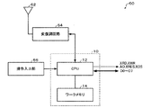
図3に、図1に示すMPU10及び表示ユニット20を携帯電話機に搭載した例を示す。MPU10は、携帯電話機(広義には電子機器)60の制御を司る中央処理装置(Central Processing Unit:CPU)12を有し、このCPU12にはワークメモリ14が接続されている。携帯電話機60には、アンテナ62を介して受信された信号を復調し、或いはアンテナ62を介して送信される信号を変調する変復調回路64が設けられている。携帯電話機60でのデータ送受信や表示パネル22の表示操作(例えばスクロール操作)などに必要な操作情報は、操作入力部66を介して入力される。
【0036】
アンテナ62から入力される信号は、変復調回路64を介して復調されてCPU12において信号処理される。CPU12は、操作入力部66からの情報等に基づき、必要によりワークメモリ14を用いて、表示パネル22の表示を行うための各種表示コマンド、或いは表示データを表示ユニット20に出力する。表示コマンドとしては、表示パネル22を駆動する表示ドライバ24の動作制御するための各種モード設定するコマンドや、表示パネル22の表示エリア上にウィンドウ表示を行う領域を例えばスタートアドレスSA及びエンドアドレスEAにより特定される矩形領域として設定するコマンド等がある。
【0037】
携帯電話機60に代表される本実施形態における電子機器では、以下に述べる構成の表示ドライバ24を適用することで、いわゆる縦方向のスクロール表示のみならず、いわゆる横方向のスクロール表示を実現し、かつ消費電力の増加を抑えることができる。
【0038】
図4に、表示ドライバ24の構成の要部のブロック図を示す。図4では、表示データRAMからの表示データの読み出しに関わる構成が示されている。また表示データRAMを構成する各メモリセルが1ピクセルの表示データを記憶するものとし、表示データが伝送される信号線の図示を簡略化している。
【0039】
表示ドライバ24は、表示データRAM28と、表示アドレスデコーダ100と、表示カラムアドレスデコーダ110と、スクロール表示データ生成回路120と、駆動回路130とを含む。
【0040】
表示データRAM28は、複数のワードラインDW1〜DWN(Nは2以上の整数)と、複数のカラムラインDC1〜DCM(Mは2以上の整数)と、各メモリセルが1ピクセル分の表示データを記憶する複数のメモリセルMC1−1〜MCM−Nとを有する。1ピクセルがR,G,Bの各6ドットで構成される場合、各メモリセルは、18ビットの表示データを記憶する。各メモリセルの配列は、表示パネルの各ピクセルの配列に対応し、各メモリセルは、ワードラインと、カラムラインとにより特定される。ワードライン方向に配列されるメモリセル群(図4においてメモリセルMC1−i〜MCM−i)は、共通のワードラインDWi(1≦i≦N、iは整数)により指定される。カラムライン方向に配列されるメモリセル群(図4においてメモリセルMCj−1〜MCj−N)は、共通のカラムラインDCj(1≦j≦M、jは整数)により指定される。
【0041】
またカラムライン方向に配列されるメモリセル群は、読出用ビットラインに共通接続される。例えば、カラムラインDCjにより指定されるメモリセル群(メモリセルMCj−1〜MCj−N)は、読出用ビットラインRBjに共通接続される。読出用ビットラインRBjには、ワードライン及びカラムラインにより指定された1つのメモリセルから読み出された1ピクセル分の表示データが出力される。
【0042】
スクロール表示データ生成回路120は、各データラッチが表示パネル22の各データラインに対応して設けられた複数のデータラッチDLAT1〜DLATx(xは2以上の整数)を含む。データラッチDLAT1〜DLATxの各データラッチは、Dフリップフロップ(DFF)により構成することができる。この場合、DFFは、クロック(C)端子への入力信号に基づいて、データ入力(D)端子への入力信号を保持し、データ出力(Q)端子から出力する。
【0043】
そして、スクロール表示データ生成回路120は、各読出用ビットラインに出力された1ピクセルの表示データごとに、該表示データを所与のスクロール量に対応したシフト量でシフトして複数のデータラッチのいずれかに取り込んで一水平走査分の表示データを生成する。
【0044】
駆動回路130は、スクロール表示データ生成回路120によって生成された一水平走査分の表示データに基づいて表示パネル22のデータラインを駆動する。より具体的には、駆動回路130は、各データライン駆動回路が表示パネル22の各データラインに対応して設けられた複数のデータライン駆動回路130−1〜130−xを含む。データライン駆動回路130−k(1≦k≦x、kは整数)は、データラッチDLATkに取り込まれた1ピクセルの表示データに対応した駆動電圧をデータラインに出力する。
【0045】
スクロール表示データ生成回路120は、複数の読出用ビットラインRB1〜RBMに接続されたスクロールバス122を含むように構成されてもよい。この場合、データラッチDLAT1〜DLATxの各D端子が、スクロールバス122に共通に接続される。そして、データラッチDLAT1〜DLATxの各C端子に入力されるクロックにより、データラッチDLAT1〜DLATxには一水平走査分の表示データが保持される。
【0046】
このようにスクロール表示データ生成回路120においてスクロールバス122にデータラッチDLAT1〜DLATxが接続される場合、スクロール表示データ生成回路120は、シフトレジスタ124を含むように構成されてもよい。この場合、データラッチDLAT1〜DLATxのC端子に入力されるクロックとして、シフトレジスタの各段のシフト出力が採用される。シフトレジスタ124は、各ラッチが各データラッチに対応して設けられた複数のラッチLAT−1〜LAT−xを含み、ラッチの出力(O)端子が次段のラッチの入力(I)端子に接続されるように構成される。ラッチは、クロック(C)端子への入力信号に基づいて、I端子への入力信号を取り込み、O端子から出力する。複数のラッチLAT−1〜LAT−xのそれぞれのC端子には、所与のシフトクロックSCLKが共通に供給される。
【0047】
したがって、初段のラッチLAT−1のI端子へのシフト入力信号SINがシフトクロックに同期してシフトされたシフト出力が、次段のラッチのI端子に順次入力されていくと共に、ラッチLAT−1〜LAT−xのO端子からシフト出力SFO1〜SFOxが順次出力される。こうすることで、データラッチDLAT1〜DLATxに対して、順次シフトされるパルスや、順次シフトされる立ち上がりエッジ又は立ち下がりエッジを供給することができる。例えば表示データRAM28からの表示データの読み出しタイミングに対応してシフトクロックSCLKを与えることで、シフトレジスタ124は、表示データRAM28から1ピクセル分ずつ読み出される表示データを取り込むためのシフト出力SFO1〜SFOxを順次出力することができる。
【0048】
更にスクロール表示データ生成回路120は、ラインラッチ128を含むように構成されてもよい。この場合、ラインラッチ128は、各DFFがデータライン駆動回路に対応して設けられた複数のDFF128−1〜128−xを含む。DFF128−kのD端子には、データラッチDLATkのQ端子が接続される。DFF128−kのC端子には、ラッチパルスLPが入力される。ラッチパルスLPは、一水平走査期間を規定する信号である。DFF128−kに保持された表示データは、データライン駆動回路130−kに供給される。このようなラインラッチ128は、ラッチパルスLPに同期して、一水平走査周期で、データラッチDLAT1〜DLATxに取り込まれた表示データを取り込む。ラインラッチ128を設けることにより、データラッチDLAT1〜DLATxは、現在の表示ラインの駆動期間に、現在の表示ラインの次の表示ラインについての表示データを取り込むことができる。
【0049】
図4に示す表示ドライバ24は、表示データRAM28に書き込まれた1フレーム分の表示データを用いて、横方向(左右方向)にピクセル単位でスクロールした表示データを生成し、該表示データに基づいてデータラインを駆動することができる。ここで横方向は、水平走査方向をいう。したがって、縦方向は、垂直走査方向ということができる。
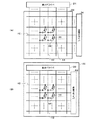
【0050】
図5に、スクロール方向を説明するための図を示す。ここでは、表示パネル22に表示される画像200を基準画像とし、該表示パネル22を正面から見た場合の横スクロール及び縦スクロールについて説明する。
【0051】
基準画像としての画像200に対し、横スクロールのうち左スクロールを行うと、表示パネル22に表示される画像は、図5に示すように画像200を左方向にシフトした画像200−Lとなる。基準画像としての画像200に対し、横スクロールのうち右スクロールを行うと、表示パネル22に表示される画像は、図5に示すように画像200を右方向にシフトした画像200−Rとなる。
【0052】
基準画像としての画像200に対し、縦スクロールのうち上スクロールを行うと、表示パネル22に表示される画像は、図5に示すように画像200を上方向にシフトした画像200−Uとなる。基準画像としての画像200に対し、縦スクロールのうち下スクロールを行うと、表示パネル22に表示される画像は、図5に示すように画像200を下方向にシフトした画像200−Dとなる。
【0053】
また基準画像としての画像200を反転した画像200−Xに対して、横スクロールや縦スクロールを行ってもよい。画像200−Xは、図4におけるシフトレジスタ124のシフト方向を反転させたり、該シフト方向はそのままで表示データRAM28の一水平走査ラインの表示データの並び順序を変更したり、或いは表示カラムアドレスのインクリメント方向を反転することで得られる。この場合、いわゆる横方向にスクロールした画像の表示反転も可能となる。
【0054】
なお図5では、スクロール後の画像200−L、200−R、200−U、200−Dは、画像200の表示部分のみを示している。例えば表示データRAM28に、表示パネル22の表示領域より大きな領域の表示データを記憶させ、スクロール後の画像200−L、200−R、200−U、200−Dにおいて画像200の表示部分以外の部分を新たに表示させてもよい。
【0055】
表示ドライバ24では、図1における走査ドライバ26の走査タイミングを変更することなく、上述の縦スクロール及び横スクロールを実現することができる。
【0056】
縦スクロールは、縦方向のスクロール量に対応して1フレームの先頭表示ラインを変更することで実現できる。より具体的には、縦方向のスクロール量に対応して、1フレームの先頭表示ラインとして表示アドレスデコーダ100に入力される表示アドレスを指定する。縦方向のスクロール量は、例えば図3に示す操作入力部66からの操作情報により指定される。
【0057】
横スクロールは、表示アドレスデコーダ100により選択されたワードラインに対応する表示ラインについて、表示データRAM28から読み出されるm(1≦m≦x、mは整数)カラムの1ピクセル分の表示データを、横方向のスクロール量に対応したm1(1≦m1≦x、m1はm以外の整数)カラムのデータラッチDLATm1に取り込むことで実現できる。図4では、表示カラムアドレスデコーダ110の入力タイミングと、シフトレジスタ124のシフト入力信号の入力タイミングとを、横方向のスクロール量に対応して互いにずらすことで実現できる。横方向のスクロール量は、例えば図3に示す操作入力部66からの操作情報により指定される。
【0058】
また縦スクロール及び横スクロールを組み合わせることで、更に斜め右上、斜め右下、斜め左上、斜め左下の各方向のスクロールを実現することもできる。
【0059】
図6に、図4における表示ドライバの横スクロールのタイミングの一例を示す。ここでは、ワードラインDW1が選択され、1カラムだけ右方向にスクロールする場合のタイミング例を示している。またシフトレジスタ124が出力するシフト出力SFO1〜SFOxにより、立ち上がりエッジを順次シフトさせている。
【0060】
例えばホストからの表示アドレスDA1が入力されると、表示アドレスデコーダ100は、表示アドレスDA1に対応するワードラインDW1を選択する。図6においては、ワードラインDW1が「H」レベルになる。
【0061】
続いて表示カラムアドレスCA1、CA2、・・・が順次入力されると、表示カラムアドレスデコーダ110は、表示カラムアドレスCA1、CA2、・・・に対応するカラムラインDC1、DC2、・・・を順次選択する。図6においては、選択されたカラムラインが「H」レベルになる。
【0062】
したがって、表示データRAM28では、まずワードラインDW1とカラムラインDC1とにより、メモリセルMC1−1が指定される。その後、表示データRAM28では、ワードラインDW1とカラムラインDC2とによりメモリセルMC2−1、ワードラインDW1とカラムラインDC3とによりメモリセルMC3−1、・・・が順次指定される。
【0063】
またカラムラインDCjにより指定される複数のメモリセルMCj−1〜MCj−Nには、読出用ビットラインRBjが共通接続される。したがって、メモリセルMC1−1が指定されると、該メモリセルMC1−1に保持された1ピクセル分の表示データD1−1が、読出用ビットラインRB1に出力される。またメモリセルMC2−1が指定されると、該メモリセルMC2−1に保持された1ピクセル分の表示データD2−1が、読出用ビットラインRB2に出力される。更にメモリセルMC3−1が指定されると、該メモリセルMC3−1に保持された1ピクセル分の表示データD3−1が、読出用ビットラインRB3に出力される。読出用ビットラインRB1〜RBMに出力された表示データは、スクロールバス122に出力される。
【0064】
また表示アドレスDA1、表示カラムアドレスCA1、CA2、・・・の入力タイミングに対して、横方向のスクロール量に対応したタイミングでシフト入力信号SINが入力される。シフトレジスタ124は、シフトクロックSCLKに同期して、例えば図6に示すようにシフト出力SFO1〜SFOxを出力する。
【0065】
データラッチDLAT1〜DLATxは、シフト出力SFO1〜SFOxの立ち上がりエッジでスクロールバス122上の表示データを取り込む。したがって、データラッチDLAT2はスクロールバス122上の表示データD1−1を取り込み、データラッチDLAT3はスクロールバス122上の表示データD2−1を取り込み、データラッチDLAT4はスクロールバス122上の表示データD3−1を取り込む。なお図6において、シフト出力SFO1の立ち上がりエッジのタイミングで、スクロールバス122上に非表示用の所与のデータを出力させたり、他のカラムラインの表示データを出力させてもよい。
【0066】
このようにしてデータラッチDLAT1〜DLATxに取り込まれた一水平走査分の表示データは、ラッチパルスLPに基づきラインラッチ128に保持される。ラインラッチ128を構成する複数のDFF128−1〜128−xの各DFFに取り込まれた表示データは、各DFFに対応して設けられたデータライン駆動回路に出力される。
【0067】
図6では、正論理でワードライン及びカラムラインが活性化されるものとして説明したが、負論理であってもよい。
【0068】
以上のように、表示ドライバ24では、複数のワードラインのいずれか1つのワードライン及び複数のカラムラインのいずれか1つのカラムラインによりメモリセルが指定される。そして、該メモリセルに記憶された1ピクセル分の表示データが、指定されたメモリセルに共通接続された読出用ビットラインを介してスクロールバスに出力される。スクロールバス上に出力された表示データは、複数のデータラッチのいずれかに取り込まれる。これらを1ピクセル単位で行ってデータラッチに一水平走査分の表示データを取り込んだ後、該一水平走査分の表示データに基づいて表示パネルのデータラインが駆動される。
【0069】
次に、本実施形態における表示ドライバ24が適用されたXドライバIC400の詳細な構成について説明する。
【0070】
図7に、XドライバIC400の詳細な構成例を示す。XドライバIC400の入出力回路として、MPUインターフェース500と入出力バッファ502とが設けられている。MPUインターフェース500には、反転チップセレクト信号XCS、コマンド/データの識別信号A0、反転リード信号XRD、反転ライト信号XWR、反転リセット信号XRESなどが入力される。入出力バッファ502には、例えば8ビットのコマンド又は表示データD0〜D7が入力される。XドライバIC400には、MPUインターフェース500及び入出力バッファ502に接続されたバスライン510が設けられている。
【0071】
バスライン510にはバスホールダ512とコマンドデコーダ514とが接続されている。なお、入出力バッファ502にはステータス設定回路516が接続され、XドライバIC400の動作状態がMPU10に出力されるようになっている。バスライン510は、表示データRAM520のI/Oバッファ562に接続され、表示データRAM520に対して読み出し、書き込みされる表示データが伝送される。表示データRAM520は、図4に示す表示データRAM28に相当する。
【0072】
XドライバIC400には、上述した表示データRAM520、I/Oバッファ562の他に、MPU系制御回路530、ロウアドレスデコーダ540、カラムアドレスデコーダ550、ドライバ系制御回路570、スクロール表示データ生成回路580、PWMデコーダ回路590及び液晶駆動回路592などが設けられている。スクロール表示データ生成回路580は、図4に示すスクロール表示データ生成回路120に相当する。
【0073】
MPU系制御回路530は、コマンドデコーダ514を介して入力されるMPU10の表示コマンドに基づいて、表示データRAM520に対する読み出し、書き込み動作を制御する。このMPU系制御回路530により制御されるロウアドレスデコーダ540及びカラムアドレスデコーダ550が設けられている。ロウアドレスデコーダ540及びカラムアドレスデコーダ550により指定されたメモリセルに、MPU10から供給された表示データが書き込まれる。また、ロウアドレスデコーダ540及びカラムアドレスデコーダ550により指定されたメモリセルからMPU10に対して表示データが読み出される。
【0074】
またXドライバIC400は、ドライバ系制御回路570により制御され表示アドレスをデコードして1ライン毎に読み出しラインを指定する表示アドレスデコーダ556を含んでいる。表示アドレスデコーダ556は、図4に示す表示アドレスデコーダ100と同様の機能を有する。更にXドライバIC400は、MPU系制御回路530又はドライバ系制御回路570により制御され、表示カラムアドレスをデコードして、表示ラインのカラムを指定する表示カラムアドレスデコーダ552を含む。表示カラムアドレスデコーダ552は、図4に示す表示カラムアドレスデコーダ110に相当する。
【0075】
ドライバ系制御回路570は、Xドライバ系制御回路572及びYドライバ系制御回路574を含む。このドライバ系制御回路570は、発振回路576からの発振出力に基づいて階調制御パルスGCP、極性反転信号FR、ラッチパルスLPなどを発生し、表示アドレスデコーダ556、スクロール表示データ生成回路580、PWMデコーダ回路590、電源制御回路578及びYドライバIC26を制御する。
【0076】
スクロール表示データ生成回路580は、表示アドレスデコーダ556及び表示カラムアドレスデコーダ552により指定された表示データRAM520のメモリセルに記憶された表示データを1ピクセルずつ読み出して、横方向のスクロール量に対応してシフトされたスクロール表示データを生成する。
【0077】
PWMデコーダ回路590は、該スクロール表示データをラッチして、極性反転周期に従って階調値に応じたパルス幅の信号を出力する。
【0078】
液晶駆動回路592は、PWMデコーダ回路590からの信号を、LCD表示系の電圧に応じた電圧にシフトさせ、表示パネル22のデータラインに供給する。液晶駆動回路592は、図4に示す駆動回路130に相当する。
【0079】
XドライバIC400では、モード切替信号により、通常モード又は横スクロールモードが切り替え可能に構成されている。通常モードでは、上述した横方向のスクロール後の表示データの生成機能がオフされる。横スクロールモードでは、上述した横方向のスクロール後の表示データの生成機能がオンされる。
【0080】
以下では、表示データRAM520と、表示データを読み出すための周辺回路とについて説明する。
【0081】
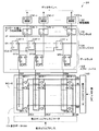
図8に、表示データRAM520の構成の概要を示す。ここでは、説明の簡略化のために、1ピクセルが4ビットで構成され、表示データRAM520が16ピクセル分の表示データを記憶する容量を有するものとする。すなわち、表示データRAM520は、各メモリセルが1ピクセル分の表示データを記憶する複数のメモリセルRAM0〜RAMFを有する。
【0082】
また表示データRAM520は、ワードラインWORD0〜WORD3と、カラムラインCOL0〜COL3を有する。ワードラインWORD0〜WORD3は、それぞれ表示アドレスデコーダ556により選択される。カラムラインCOL0〜COL3は、それぞれ表示カラムアドレスデコーダ552により選択される。
【0083】
メモリセルRAM0〜RAM3は、ワードラインWORD0により指定される。メモリセルRAM4〜RAM7は、ワードラインWORD1により指定される。メモリセルRAM8〜RAMBは、ワードラインWORD2により指定される。メモリセルRAMC〜RAMFは、ワードラインWORD3により指定される。メモリセルRAM0、RAM4、RAM8、RAMCは、カラムラインCOL0により指定される。メモリセルRAM1、RAM5、RAM9、RAMDは、カラムラインCOL1により指定される。メモリセルRAM2、RAM6、RAMA、RAMEは、カラムラインCOL2により指定される。メモリセルRAM3、RAM7、RAMB、RAMFは、カラムラインCOL3により指定される。
【0084】
またメモリセルRAM0、RAM4、RAM8、RAMCには、読出用ビットラインBIT0が接続される。メモリセルRAM1、RAM5、RAM9、RAMDには、読出用ビットラインBIT1が接続される。メモリセルRAM2、RAM6、RAMA、RAMEには、読出用ビットラインBIT2が接続される。メモリセルRAM3、RAM7、RAMB、RAMFには、読出用ビットラインBIT3が接続される。
【0085】
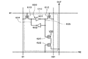
図9に、各メモリセルを構成する1ビットのRAMセルの回路図を示す。RAMセルC10は、他のRAMセルと同一の構成を有する。このRAMセルC10は、2つのCMOSインバータ601、602にて構成されるメモリ素子600を有する。2つのCMOSインバータ601、602は、その入出力同士を互いに接続する第1及び第2の配線604、606を有する。第1の配線604とビット線B1との間には第1のN型MOSトランジスタ610が接続される。第1のN型MOSトランジスタ610のゲートは第1のワード線W1に接続されている。同様に、第2の配線606とビット線XB1との間には第2のN型MOSトランジスタ612が接続される。第2のN型MOSトランジスタ612のゲートは第1のワード線W1に接続されている。
【0086】
このようなRAMセルにおいて、ロウアドレスデコーダ540からのアクティブ信号により第1のワード線W1が「H」レベル(第1のワード線W1の電圧に対応する論理レベルが「H」レベル)になると、第1及び第2のN型MOSトランジスタ610、612がオンになる。これにより、RAMセルC10は一対のビット線B1、XB1と接続される。このとき、カラムアドレスデコーダ550によりRAMセルC10が選択されていると、RAMセルC10に対するデータの読み出し、又は書き込みが可能となる。
【0087】
また、電源供給線VDDと表示データ出力線OUTとの間には第1及び第2のP型MOSトランジスタ620、622が接続されている。第1のP型MOSトランジスタ620のゲートは第2の配線606に接続される。第2のP型MOSトランジスタ622のゲートは第2のワード線W2に接続されている。
【0088】
RAMセルC10のデータを読出用ビットラインとしての表示データ出力線OUTに読み出す前に、この表示データ出力線OUTは「L」レベル(表示データ出力線OUTの電圧に対応する論理レベルが「L」レベル)にプリチャージされている。そして、このプリチャージ動作後に、表示アドレスデコーダ556によって選択されたワードラインと、表示カラムアドレスデコーダ552によって選択されたカラムラインとにより、第2のワード線W1を「L」レベルとする。これにより、第2のP型MOSトランジスタ622がオンとなり、表示データ出力線OUTのデータがPWMデコーダ回路590にてラッチされる。このとき、第2の配線606の論理レベルが「H」レベル(第1の配線604の論理レベルが「L」レベル)であれば表示データ出力線OUTは「L」レベルのままである。一方、第2の配線606の論理レベルが「L」レベル(第1の配線604の論理レベルが「H」レベル)であれば表示データ出力線OUTは「H」レベルとなる。
【0089】
図10に、スクロール表示データ生成回路580の回路図を示す。スクロール表示データ生成回路580は、セレクタ700、シフトレジスタ710、データラッチ720、ラインラッチ730を含む。
【0090】
セレクタ700は、モード切替信号HSC_ENAに応じて、通常モード用の表示データ、又は横スクロールモード用の表示データを、データラッチ720に対して出力する。
【0091】
シフトレジスタ710は、モード切替信号HSC_ENAに応じて、通常モード用にデータラッチ720で表示データを取り込むためのラッチクロック、又は横スクロールモード用にデータラッチ720で表示データを取り込むためのシフト出力を、データラッチ720に対して出力する。シフトレジスタ710は、図4に示すシフトレジスタ124と同様の機能を含む。
【0092】
ラインラッチ730は、データラッチ720に取り込まれた一水平走査分の表示データを取り込む。ラインラッチ730は、図4に示すラインラッチ128と同様の機能を有する。
【0093】
なお図10において、ラッチクロックDLT_LINE、シフトクロックSCLK、シフト信号LE、RI、シフト方向切替信号SHL、セット信号SETが、シフトレジスタ710に入力される。
【0094】
図11に、セレクタ700の回路図を示す。セレクタ700は、デマルチプレクサDMPX0〜DMPX3と、スクロールバス708と、マルチプレクサMPX0〜MPX3とを含む。デマルチプレクサDMPX0〜DMPX3は、それぞれ同一構成をなしている。マルチプレクサMPX0〜MPX3は、それぞれ同一構成をなしている。
【0095】
カラムラインCOL0により指定されるカラム0について、デマルチプレクサDMPX0は、モード切替信号HSC_ENAに応じて、マルチプレクサMPX0、又はスクロールバス708に、読出用ビットラインBIT0の信号を出力する。より具体的には、モード切替信号HSC_ENAにより通常モードに切り替えられているとき、デマルチプレクサDMPX0は、読出用ビットラインBIT0の信号をマルチプレクサMPX0に出力する。またモード切替信号HSC_ENAにより横スクロールモードに切り替えられているとき、デマルチプレクサDMPX0は、読出用ビットラインBIT0の信号をスクロールバス708に出力する。
【0096】
スクロールバス708は、図4に示すスクロールバス122に相当し、デマルチプレクサDMPX0〜DMPX3に共通に接続される。なおスクロールバス708は、マルチプレクサMPX0〜MPX3にも共通に接続される。
【0097】
マルチプレクサMPX0は、モード切替信号HSC_ENAに応じて、デマルチプレクサDMPX0からの信号、又はスクロールバス708上の信号を、選択出力する。より具体的には、モード切替信号HSC_ENAにより通常モードに切り替えられているとき、マルチプレクサMPX0は、デマルチプレクサDMPX0からの信号を選択出力する。またモード切替信号HSC_ENAにより横スクロールモードに切り替えられているとき、マルチプレクサMPX0は、スクロールバス708上の信号を選択出力する。
【0098】
図12に、シフトレジスタ710の回路図を示す。シフトレジスタ710は、複数のラッチLLAT0〜LLAT3を含み、シフト方向切替信号SHLによって指定されるシフト方向に応じてそのシフト方向が切り替えられる。シフトレジスタ710は、シフトクロックSCLKに基づき、シフト信号LE又はシフト信号RIをシフトする。なお図12では、セット信号SETによって設定される立ち上がりエッジが、順次シフトされる。
【0099】
図13に、シフトレジスタ710を構成するラッチLLAT0の回路図を示す。なおラッチLLAT0〜LLAT3は、それぞれ同一の構成をなしている。図13に示すようにラッチLLAT0は、シフト方向切替信号SHLが「H」レベルのとき、シフトクロックSCLKに同期して、シフト信号RIを入力とし、シフト信号LEを出力する。またラッチLLAT0は、シフト方向切替信号SHLが「L」レベルのとき、シフトクロックSCLKに同期して、シフト信号LEを入力とし、シフト信号RIを出力する。
【0100】
ラッチLLAT0では、セット信号SETを「H」レベルにしてノードNDを「L」レベルにした後、シフト動作が行われる。
【0101】
図12において、シフトレジスタ710は、モード切替信号HSC_ENAに応じて、ラッチLLAT0〜LLTA3からのラッチ出力DLATCH_COL0〜DLATCH_COL3、又はラッチクロックDLATCH_LINEを出力する。より具体的には、モード切替信号HSC_ENAにより通常モードに切り替えられているとき、シフトレジスタ710は、ラッチクロックDLATCH_LINEをシフト出力として出力する。またモード切替信号HSC_ENAにより横スクロールモードに切り替えられているとき、シフトレジスタ710は、ラッチ出力DLATCH_COL0〜DLATCH_COL3をシフト出力として出力する。
【0102】
図14に、データラッチ720の回路図を示す。データラッチ720は、シフトレジスタ710のシフト出力に基づき、セレクタ700から選択出力された信号を取り込む。
【0103】
次に、図15及び図16を参照しながら、図8〜図14に示した表示データRAM520と、表示データを読み出すための周辺回路の動作について説明する。
【0104】
図15に、通常モードにおける動作タイミングの一例を示す。通常モードは、モード切替信号HSC_ENAにより設定される。
【0105】
通常モードでは、表示カラムアドレスデコーダ552により選択されるカラムラインは変化せず、「H」レベルに固定される。そして、表示アドレスデコーダ556によりワードラインが選択されると、該ワードラインにより指定される表示ラインの表示データが読出用ビットラインBIT0〜BIT3を介して表示データRAM520から出力される。
【0106】
セレクタ700では、読出用ビットラインBIT0〜BIT3からの表示データがそのまま選択出力される。またシフトレジスタ710では、ラッチクロックDLT_LINEがシフト出力DLT_COL0〜DLT_COL3として出力される。
【0107】
データラッチ720では、シフト出力DLT_COL0〜DLT_COL3により、1表示ライン単位で読み出された表示データが取り込まれる。ラインラッチ730は、データラッチ720に取り込まれた表示データを、ラッチパルスLPに基づき取り込んで、ラッチデータDD0〜DD3として、PWMデコーダ回路590に対して出力する。
【0108】
なお図15では、メモリセルRAMp(pは0〜Fのいずれか)に保持された表示データをpとして表わしている。
【0109】
このように通常モードでは、図8〜図14に示した構成により、表示ライン単位で表示データを読み出し、表示パネルのデータラインを駆動することができる。
【0110】
図16に、横スクロールモードにおける動作タイミングの一例を示す。図16では、1カラム分の右スクロールをしたときの動作と、2カラム分の右スクロールをしたときの動作とを示している。横スクロールモードは、モード切替信号HSC_ENAにより設定される。
【0111】
横スクロールモードでは、表示アドレスデコーダ556によりワードラインが選択され、表示カラムアドレスデコーダ552によりカラムラインが選択される。そして、該ワードライン及び該カラムラインにより指定されるメモリセルに記憶された1ピクセル分の表示データが、読出用ビットラインBIT0〜BIT3のいずれかを介して表示データRAM520から出力される。
【0112】
セレクタ700では、読出用ビットラインBIT0〜BIT3からの表示データがスクロールバス708に出力される。
【0113】
一方、シフトレジスタ710では、セット信号SETにより初期化された後に、シフトクロックSCLKに基づき、シフト信号LEが右方向にシフトされる。これにより、シフト出力DLT_COL0〜DLT_COL3による立ち上がりエッジが順次シフトされる。
【0114】
データラッチ720では、シフト出力DLT_COL0〜DLT_COL3により、スクロールバス708上の表示データが順次取り込まれ、取り込みデータDDAT0〜DDAT3としてラインラッチ730に出力される。ラインラッチ730は、ラッチパルスLPに基づき、データラッチ720に取り込まれた表示データを取り込んで、ラッチデータDD0〜DD3として、PWMデコーダ回路590に対して出力する。
【0115】
図16に示すように、XドライバIC400における横方向のスクロールを行う場合、シフトレジスタ710の動作を変更することなく、表示カラムアドレスデコーダ552によるカラムラインの選択タイミングを変更すればよい。そのため、表示カラムアドレスデコーダ552への表示カラムアドレスの供給タイミングを変更するだけでよい。こうすることで、スクロール量に対応してシフトされた表示データをラインラッチ730に取り込むことができる。
【0116】
このように横スクロールモードにおいても、図8〜図14に示した構成により、スクロール量に対応してシフトされた表示データに基づき、表示パネルのデータラインを駆動することができる。
【0117】
なお、本発明は上述した実施の形態に限定されるものではなく、本発明の要旨の範囲内で種々の変形実施が可能である。
【0118】
また上述した実施の形態では、表示パネルとしてアクティブマトリクス方式について説明したが、これに限定されるものではなく、パッシブマトリクス方式の表示パネルについても同様に適用することができる。また上述の実施形態では1表示ライン単位で駆動される例について説明したが、これに限定されるものではなく、複数のデータライン単位に読み出された表示データについても同様に適用することができる。更に上述の実施形態では、1ピクセルずつに表示データを読み出して横スクロール用の表示データを生成していたがこれに限定されるものではなく、複数ピクセルずつ読み出して横スクロール用の表示データを生成することも可能である。
【0119】
また、本発明のうち従属請求項に係る発明においては、従属先の請求項の構成要件の一部を省略する構成とすることもできる。また、本発明の1の独立請求項に係る発明の要部を、他の独立請求項に従属させることもできる。
【図面の簡単な説明】
【図1】本実施形態の電気光学装置を含む電子機器の概略ブロック図。
【図2】図2(A)、(B)は表示パネルの構成例の等価回路図。
【図3】図1に示すMPU及び表示ユニットを携帯電話機に搭載した例のブロック図。
【図4】表示ドライバの構成の要部のブロック図。
【図5】スクロール方向の説明図。
【図6】横スクロールを行った場合のタイミングの一例を示す図。
【図7】XドライバICの詳細な構成例のブロック図。
【図8】表示データRAMの構成の概要を示す回路図。
【図9】各メモリセルを構成する1ビットのRAMセルの回路図。
【図10】図8に示すスクロール表示データ生成回路の回路図。
【図11】図10に示すセレクタの回路図。
【図12】図10に示すシフトレジスタの回路図。
【図13】図12に示すラッチの回路図。
【図14】図10に示すデータラッチの回路図。
【図15】通常モードにおける動作例のタイミング図。
【図16】横スクロールモードにおける動作例のタイミング図。
【符号の説明】
24 表示ドライバ、28 表示データRAM、
100 表示アドレスデコーダ、110 表示カラムアドレスデコーダ、
120 スクロール表示データ生成回路、122 スクロールバス、
124 シフトレジスタ、128 ラインラッチ、
128−1〜128−x DFF、130 駆動回路、
130−1〜130−x データライン駆動回路、
DC1〜DNM カラムライン、DLAT1〜DLATx データラッチ、
DW1〜DWN ワードライン、LAT1〜LATx ラッチ、
LP ラッチパルス、 MC1−1〜MCM−N メモリセル、
RB1〜RBM 読出用ビットライン、SFO1〜SFOx シフト出力、
SCLK シフトクロック、SIN シフト入力信号[0001]
TECHNICAL FIELD OF THE INVENTION
The present invention relates to a display driver, an electro-optical device, an electronic device, and a display driving method.
[0002]
[Prior art]
A display panel (electro-optical device in a broad sense) represented by an LCD (liquid crystal display) panel is mounted on a mobile phone or a portable information terminal (Personal Digital Assistants: PDA). In particular, the LCD panel realizes smaller size, lower power consumption, and lower cost than other display panels, and is mounted on various electronic devices.
[0003]
The LCD panel includes, for example, a plurality of scan lines, a plurality of data lines, and a plurality of pixels connected to the scan lines and the data lines. The data lines of the LCD panel are driven by the display driver based on the display data. The scan lines of the LCD panel are scanned by a scan driver.
[0004]
The display driver can reduce power consumption by incorporating a display data RAM that stores display data for one frame, for example. The display data is supplied to the display driver by a host such as an external MPU (Micro Processor Unit). The display data RAM includes a plurality of memory cells. In the display data RAM, the arrangement of each memory cell corresponds to the arrangement of pixels of the LCD panel. In each memory cell, display data of, for example, one pixel from the host is written. For example, display data is read out, for example, in units of one display line from a display data RAM in which display data for one frame is written, and used for driving data lines of an LCD panel (see Patent Document 1).
[0005]
Therefore, display data is read out from the display data RAM in units of display lines, and it has been difficult to scroll the display screen of the LCD panel in the display line direction. For example, if the vertical scanning direction is the vertical direction of the display screen, vertical scroll display can be performed, but horizontal scroll display has been difficult. When the display driver incorporating the display data RAM realizes the horizontal scroll display, the host newly writes the display data of the image after the horizontal scroll into the display data RAM, or stores the display data in the display data RAM internally. (See Patent Document 2).
[0006]
[Patent Document 1]
WO00 / 02189
[Patent Document 2]
JP-A-9-265274
[0007]
[Problems to be solved by the invention]
However, when the display driver incorporating the display data RAM realizes the horizontal scroll display, if the host newly writes the display data of the image after the horizontal scroll into the display data RAM, the consumption associated with the interface between the display driver and the host is increased. There is a problem of increasing power. Therefore, there is no point in incorporating the display data RAM into the display driver.
[0008]
In a display driver incorporating a display data RAM, if the display data of the image after horizontal scrolling is rewritten inside the display driver as described in
[0009]
The present invention has been made in view of the above technical problems, and an object of the present invention is to provide a display driver and an electro-optical device capable of performing a so-called horizontal scroll display while suppressing an increase in power consumption. , An electronic device, and a display driving method.
[0010]
[Means for Solving the Problems]
In order to solve the above-mentioned problem, the present invention is a display driver for driving a data line of an electro-optical device on the basis of display data, wherein a plurality of word lines, a plurality of column lines, and each memory cell correspond to one pixel. A display data RAM having a plurality of memory cells for storing display data, a display address decoder for selecting a word line of the display data RAM based on a display address, and a column of the display data RAM based on a display column address. A display column address decoder for selecting a line, a plurality of read bit lines provided corresponding to each column line, and a plurality of read bit lines commonly connected to a memory cell group specified by the column line; A scroll bus connected to the read bit line; and a data bus of the electro-optical device. A plurality of data latches, each data latch provided corresponding to each of the data latches, taking in display data on the scroll bus; and a driving circuit driving the data line based on the display data taken in by the plurality of data latches. And reads one pixel of display data from one memory cell specified by the word line selected by the display address decoder and the column line selected by the display column address decoder, and stores the display data in the memory. A display driver outputs to the scroll bus via a read bit line connected to a cell, and each data latch of the plurality of data latches captures display data on the scroll bus.
[0011]
In the present invention, display data read from memory cells constituting the display data RAM is output to a scroll bus, and display data on the scroll bus is transferred to one of a plurality of data latches commonly connected to the scroll bus. I try to take in. Therefore, the data line can be driven based on the display data after scrolling according to an arbitrary scroll amount in the horizontal scanning direction without rewriting the display data stored in the display data RAM. Therefore, a clock for reading out one frame of display data generated at the time of rewriting and a clock for rewriting one frame of updated display data to the display data RAM are not required, thereby increasing power consumption. Thus, a so-called horizontal scroll display can be realized.
[0012]
Further, by using together with a so-called vertical scroll which is realized by changing a word line selected by the display address decoder, scrolling in an oblique direction can be easily realized with low power consumption.
[0013]
Further, the display driver according to the present invention includes a shift register that outputs a shift output shifted based on a given shift clock, wherein each data latch of the plurality of data latches is a shift output of each stage of the shift register. , The display data on the scroll bus can be captured.
[0014]
According to the present invention, the display data for scrolling corresponding to an arbitrary scroll amount can be generated by the read timing of the display data from the display data RAM and the output timing of the shift output output from the shift register. . Therefore, it is possible to achieve so-called horizontal scrolling while achieving both simplification of the circuit and low power consumption.
[0015]
Further, in the display driver according to the present invention, the display driver includes a line latch that captures the display data captured by the plurality of data latches in one horizontal scanning cycle, and the driving circuit includes the line latch instead of the plurality of data latches. The data line can be driven based on the acquired display data.
[0016]
According to the present invention, the display data captured by the plurality of data latches is not overwritten by the next scrolled display data, so that the next display line after the current display line is driven during the current display line driving period. Display data for the display line can be captured.
[0017]
The present invention is also a display driver for driving a data line of an electro-optical device based on display data, wherein a plurality of word lines, a plurality of column lines, and each memory cell stores display data for one pixel. A display data RAM having a plurality of memory cells, a display address decoder for selecting a word line of the display data RAM based on a display address, and a display column for selecting a column line of the display data RAM based on a display column address An address decoder, a plurality of read bit lines in which each read bit line is commonly connected to a memory cell designated by a column line, and each data latch are provided corresponding to each data line of the electro-optical device. It has a plurality of data latches, and is equivalent to one pixel output to each read bit line. A scroll display data generation circuit that shifts the display data by a shift amount corresponding to a given scroll amount and takes in one of the plurality of data latches to generate display data for one horizontal scan for each of the display data; And a drive circuit for driving the data lines based on display data for one horizontal scan generated by the scroll display data generation circuit.
[0018]
The present invention also provides a plurality of scan lines, a plurality of data lines, a plurality of pixels connected to the plurality of scan lines and the plurality of data lines, a scan driver for scanning the plurality of scan lines, A display driver according to any one of the above, which drives the plurality of data lines.
[0019]
The present invention also provides a display panel including a plurality of scan lines, a plurality of data lines, a plurality of pixels connected to the plurality of scan lines and the plurality of data lines, and scanning the plurality of scan lines. The present invention relates to an electro-optical device including a scan driver for driving the plurality of data lines and a display driver for driving the plurality of data lines.
[0020]
According to the present invention, it is possible to provide an electro-optical device that realizes horizontal scrolling with low power consumption.
[0021]
The present invention also relates to an electronic apparatus including the above-described electro-optical device and a display data generation unit that generates display data supplied to the electro-optical device.
[0022]
ADVANTAGE OF THE INVENTION According to this invention, it can contribute to provision of the electronic device which implement | achieves horizontal scrolling of an image with low power consumption.
[0023]
Further, the present invention is based on display data read from a display data RAM having a plurality of word lines, a plurality of column lines, and a plurality of memory cells each of which stores display data for one pixel. A display driving method for driving a data line of an electro-optical device, wherein a memory cell is specified by one of the plurality of word lines and one of the plurality of column lines. The display data for one pixel stored in the cell is output to a scroll bus via a read bit line commonly connected to a memory cell group specified by the one column line, and each data latch is connected to the electro-optical device. One of a plurality of data latches provided corresponding to each data line of the device, Captures display data of a pixel is related to the display driving method for driving the data lines of the electro-optical device based on the display data loaded in the plurality of data latches.
[0024]
Further, in the display driving method according to the present invention, the display data for one pixel on the scroll bus is taken into each data latch of the plurality of data latches by repeating the driving several times in one horizontal scanning period. The display data for one horizontal scan may be fetched into the plurality of data latches, and the data lines of the electro-optical device may be driven based on the display data fetched into the plurality of data latches.
[0025]
BEST MODE FOR CARRYING OUT THE INVENTION
Hereinafter, preferred embodiments of the present invention will be described in detail with reference to the drawings. The embodiments described below do not unduly limit the contents of the invention described in the claims. In addition, all of the configurations described below are not necessarily essential components of the invention.
[0026]
1. Electro-optical device
FIG. 1 is a schematic block diagram of an electronic apparatus including the electro-optical device according to the present embodiment. The electronic device includes an
[0027]
The
[0028]
2A and 2B show equivalent circuits of a configuration example of the
[0029]
The
[0030]
In the
[0031]
Further, in the display panel, as shown in FIG. 2B, at least one of the
[0032]
2A and 2B, a TFD is used as an active matrix method. However, the present invention is not limited to this. For example, a three-terminal element such as a thin film transistor (TFT) or another two-terminal element may be used. An active matrix panel using terminal elements may be used.
[0033]
In FIG. 1, the
[0034]
The MPU 10 (display data generation unit in a broad sense) supplies a control signal, a display command, and display data to the
[0035]
FIG. 3 shows an example in which the
[0036]
A signal input from the
[0037]
In the electronic device according to the present embodiment represented by the
[0038]
FIG. 4 shows a block diagram of a main part of the configuration of the
[0039]
The
[0040]
The
[0041]
The memory cell groups arranged in the column line direction are commonly connected to a read bit line. For example, a memory cell group (memory cells MCj-1 to MCj-N) specified by the column line DCj is commonly connected to the read bit line RBj. Display data for one pixel read from one memory cell specified by a word line and a column line is output to the read bit line RBj.
[0042]
The scroll display data generation circuit 120 includes a plurality of data latches DLAT1 to DLATx (x is an integer of 2 or more) in which each data latch is provided corresponding to each data line of the
[0043]
Then, the scroll display data generation circuit 120 shifts the display data by a shift amount corresponding to a given scroll amount for each one-pixel display data output to each read bit line, and The data is taken into one of them and display data for one horizontal scan is generated.
[0044]
The
[0045]
The scroll display data generation circuit 120 may be configured to include a
[0046]
When the data latches DLAT1 to DLATx are connected to the
[0047]
Therefore, the shift output obtained by shifting the shift input signal SIN to the I terminal of the first-stage latch LAT-1 in synchronization with the shift clock is sequentially input to the I terminal of the next-stage latch, and the latch LAT-1 Shift outputs SFO1 to SFOx are sequentially output from the O terminals of .about.LAT-x. In this way, sequentially shifted pulses and sequentially shifted rising edges or falling edges can be supplied to the data latches DLAT1 to DLATx. For example, by providing the shift clock SCLK in accordance with the read timing of the display data from the
[0048]
Further, the scroll display data generation circuit 120 may be configured to include a
[0049]
The
[0050]
FIG. 5 shows a diagram for explaining the scroll direction. Here, horizontal scrolling and vertical scrolling when the
[0051]
When the left scroll of the horizontal scroll is performed on the
[0052]
When the upward scroll of the vertical scroll is performed on the
[0053]
Horizontal scrolling or vertical scrolling may be performed on an image 200-X obtained by inverting the
[0054]
In FIG. 5, the scrolled images 200-L, 200-R, 200-U, and 200-D show only the display portion of the
[0055]
The
[0056]
Vertical scrolling can be realized by changing the top display line of one frame according to the vertical scroll amount. More specifically, the display address input to the
[0057]
In the horizontal scroll, display data for one pixel in m (1 ≦ m ≦ x, where m is an integer) columns read from the
[0058]
Further, by combining vertical scrolling and horizontal scrolling, it is possible to further realize scrolling in each of the diagonally upper right, diagonally lower right, diagonally upper left, and diagonally lower left directions.
[0059]
FIG. 6 shows an example of the horizontal scroll timing of the display driver in FIG. Here, an example of the timing when the word line DW1 is selected and one column is scrolled rightward is shown. The rising edges are sequentially shifted by the shift outputs SFO1 to SFOx output from the
[0060]
For example, when the display address DA1 is input from the host, the
[0061]
Subsequently, when the display column addresses CA1, CA2,... Are sequentially input, the display column address decoder 110 sequentially outputs the column lines DC1, DC2,. select. In FIG. 6, the selected column line goes to “H” level.
[0062]
Therefore, in the
[0063]
A read bit line RBj is commonly connected to the plurality of memory cells MCj-1 to MCj-N specified by the column line DCj. Therefore, when the memory cell MC1-1 is designated, the display data D1-1 for one pixel held in the memory cell MC1-1 is output to the read bit line RB1. When the memory cell MC2-1 is specified, the display data D2-1 for one pixel held in the memory cell MC2-1 is output to the read bit line RB2. Further, when the memory cell MC3-1 is specified, the display data D3-1 for one pixel held in the memory cell MC3-1 is output to the read bit line RB3. The display data output to the read bit lines RB1 to RBM is output to the
[0064]
Also, the shift input signal SIN is input at a timing corresponding to the horizontal scroll amount with respect to the input timing of the display address DA1, the display column addresses CA1, CA2,. The
[0065]
The data latches DLAT1 to DLATx capture display data on the
[0066]
The display data for one horizontal scan captured by the data latches DLAT1 to DLATx in this manner is held in the
[0067]
In FIG. 6, it has been described that the word line and the column line are activated by the positive logic, but may be the negative logic.
[0068]
As described above, in the
[0069]
Next, a detailed configuration of the
[0070]
FIG. 7 shows a detailed configuration example of the
[0071]
A
[0072]
The
[0073]
The
[0074]
The
[0075]
Driver
[0076]
The scroll display
[0077]
The
[0078]
The liquid
[0079]
The
[0080]
Hereinafter, the
[0081]
FIG. 8 shows an outline of the configuration of the
[0082]
The
[0083]
Memory cells RAM0 to RAM3 are specified by word line WORD0. The memory cells RAM4 to RAM7 are specified by a word line WORD1. The memory cells RAM8 to RAMB are specified by the word line WORD2. Memory cells RAMC to RAMF are specified by word line WORD3. The memory cells RAM0, RAM4, RAM8, and RAMC are specified by the column line COL0. The memory cells RAM1, RAM5, RAM9, and RAMD are specified by the column line COL1. The memory cells RAM2, RAM6, RAMA, and RAME are specified by the column line COL2. The memory cells RAM3, RAM7, RAMB, RAMF are specified by the column line COL3.
[0084]
A read bit line BIT0 is connected to the memory cells RAM0, RAM4, RAM8, and RAMC. A read bit line BIT1 is connected to the memory cells RAM1, RAM5, RAM9, and RAMD. A read bit line BIT2 is connected to the memory cells RAM2, RAM6, RAMA, and RAME. A read bit line BIT3 is connected to the memory cells RAM3, RAM7, RAMB, and RAMF.
[0085]
FIG. 9 shows a circuit diagram of a 1-bit RAM cell constituting each memory cell. The RAM cell C10 has the same configuration as other RAM cells. This RAM cell C10 has a
[0086]
In such a RAM cell, when the first word line W1 goes high (the logic level corresponding to the voltage of the first word line W1 goes high) by the active signal from the
[0087]
Further, first and second P-
[0088]
Before the data of the RAM cell C10 is read to the display data output line OUT as a read bit line, the display data output line OUT is set to the “L” level (the logical level corresponding to the voltage of the display data output line OUT is “L”). Level). Then, after this precharge operation, the second word line W1 is set to the “L” level by the word line selected by the
[0089]
FIG. 10 is a circuit diagram of the scroll display
[0090]
The
[0091]
The
[0092]
The
[0093]
In FIG. 10, a latch clock DLT_LINE, a shift clock SCLK, shift signals LE and RI, a shift direction switching signal SHL, and a set signal SET are input to the
[0094]
FIG. 11 shows a circuit diagram of the
[0095]
For
[0096]
The scroll bus 708 corresponds to the
[0097]
The multiplexer MPX0 selectively outputs a signal from the demultiplexer DMPX0 or a signal on the scroll bus 708 according to the mode switching signal HSC_ENA. More specifically, when the mode is switched to the normal mode by the mode switching signal HSC_ENA, the multiplexer MPX0 selects and outputs the signal from the demultiplexer DMPX0. When the mode is switched to the horizontal scroll mode by the mode switching signal HSC_ENA, the multiplexer MPX0 selects and outputs a signal on the scroll bus 708.
[0098]
FIG. 12 is a circuit diagram of the
[0099]
FIG. 13 is a circuit diagram of the latch LLAT0 included in the
[0100]
In the latch LLAT0, the shift operation is performed after the set signal SET is set to “H” level and the node ND is set to “L” level.
[0101]
12, a
[0102]
FIG. 14 is a circuit diagram of the
[0103]
Next, operations of the
[0104]
FIG. 15 shows an example of operation timing in the normal mode. The normal mode is set by the mode switching signal HSC_ENA.
[0105]
In the normal mode, the column line selected by the display
[0106]
In the
[0107]
In the
[0108]
In FIG. 15, the display data held in the memory cell RAMp (p is any one of 0 to F) is represented as p.
[0109]
As described above, in the normal mode, the display data can be read in units of display lines and the data lines of the display panel can be driven by the configurations shown in FIGS.
[0110]
FIG. 16 shows an example of operation timing in the horizontal scroll mode. FIG. 16 shows an operation when the right scroll is performed by one column and an operation when the right scroll is performed by two columns. The horizontal scroll mode is set by the mode switching signal HSC_ENA.
[0111]
In the horizontal scroll mode, the
[0112]
In the
[0113]
On the other hand, in the
[0114]
In the
[0115]
As shown in FIG. 16, when performing horizontal scrolling in the
[0116]
As described above, even in the horizontal scroll mode, the data lines of the display panel can be driven based on the display data shifted according to the scroll amount by the configuration shown in FIGS.
[0117]
Note that the present invention is not limited to the above-described embodiment, and various modifications can be made within the scope of the present invention.
[0118]
Further, in the above-described embodiment, an active matrix type display panel is described as a display panel. However, the present invention is not limited to this, and can be similarly applied to a passive matrix type display panel. In the above-described embodiment, an example in which the display is driven in units of one display line has been described. However, the present invention is not limited to this. The present invention can be similarly applied to display data read in units of a plurality of data lines. . Furthermore, in the above-described embodiment, the display data for horizontal scrolling is generated by reading out the display data for each pixel. However, the present invention is not limited to this. The display data for horizontal scrolling is generated by reading out a plurality of pixels. It is also possible.
[0119]
Further, in the invention according to the dependent claims of the present invention, a configuration in which some of the constituent elements of the dependent claims are omitted may be adopted. In addition, a main part of the invention according to one independent claim of the present invention can be made dependent on another independent claim.
[Brief description of the drawings]
FIG. 1 is a schematic block diagram of an electronic apparatus including an electro-optical device according to an embodiment.
FIGS. 2A and 2B are equivalent circuit diagrams of a configuration example of a display panel.
FIG. 3 is a block diagram of an example in which the MPU and the display unit shown in FIG. 1 are mounted on a mobile phone.
FIG. 4 is a block diagram of a main part of a configuration of a display driver.
FIG. 5 is an explanatory diagram of a scroll direction.
FIG. 6 is a diagram illustrating an example of timing when horizontal scrolling is performed.
FIG. 7 is a block diagram of a detailed configuration example of an X driver IC.
FIG. 8 is a circuit diagram showing an outline of a configuration of a display data RAM.
FIG. 9 is a circuit diagram of a 1-bit RAM cell forming each memory cell.
FIG. 10 is a circuit diagram of the scroll display data generation circuit shown in FIG. 8;
11 is a circuit diagram of the selector shown in FIG.
12 is a circuit diagram of the shift register illustrated in FIG.
FIG. 13 is a circuit diagram of the latch shown in FIG. 12;
FIG. 14 is a circuit diagram of the data latch shown in FIG. 10;
FIG. 15 is a timing chart of an operation example in a normal mode.
FIG. 16 is a timing chart of an operation example in the horizontal scroll mode.
[Explanation of symbols]
24 display drivers, 28 display data RAMs,
100 display address decoder, 110 display column address decoder,
120 scroll display data generation circuit, 122 scroll bus,
124 shift register, 128 line latch,
128-1 to 128-x DFF, 130 drive circuit,
130-1 to 130-x data line driving circuit,
DC1 to DNM column line, DLAT1 to DLATx data latch,
DW1 to DWN word line, LAT1 to LATx latch,
LP latch pulse, MC1-1 to MCM-N memory cell,
RB1 to RBM read bit line, SFO1 to SFOx shift output,
SCLK shift clock, SIN shift input signal
Claims (9)
複数のワードラインと、複数のカラムラインと、各メモリセルが1ピクセル分の表示データを記憶する複数のメモリセルとを有する表示データRAMと、
表示アドレスに基づいて前記表示データRAMのワードラインを選択する表示アドレスデコーダと、
表示カラムアドレスに基づいて前記表示データRAMのカラムラインを選択する表示カラムアドレスデコーダと、
各読出用ビットラインが各カラムラインに対応して設けられカラムラインにより指定されるメモリセル群に共通接続された複数の読出用ビットラインと、
前記複数の読出用ビットラインに接続されたスクロールバスと、
前記電気光学装置の各データラインに対応して設けられた各データラッチが前記スクロールバス上の表示データを取り込む複数のデータラッチと、
前記複数のデータラッチに取り込まれた表示データに基づいて前記データラインを駆動する駆動回路とを含み、
前記表示アドレスデコーダによって選択されたワードラインと前記表示カラムアドレスデコーダによって選択されたカラムラインとにより指定された1つのメモリセルから1ピクセル分の表示データを読み出し、該表示データを前記メモリセルに接続された読出用ビットラインを介して前記スクロールバスに出力し、前記複数のデータラッチの各データラッチが前記スクロールバス上の表示データを取り込むことを特徴とする表示ドライバ。A display driver that drives a data line of the electro-optical device based on display data,
A display data RAM having a plurality of word lines, a plurality of column lines, and a plurality of memory cells each of which stores display data for one pixel;
A display address decoder for selecting a word line of the display data RAM based on a display address;
A display column address decoder for selecting a column line of the display data RAM based on a display column address;
A plurality of read bit lines, each read bit line provided corresponding to each column line and commonly connected to a memory cell group specified by the column line;
A scroll bus connected to the plurality of read bit lines;
A plurality of data latches, each data latch provided corresponding to each data line of the electro-optical device, capturing display data on the scroll bus;
A drive circuit for driving the data line based on the display data captured by the plurality of data latches,
One pixel of display data is read from one memory cell specified by the word line selected by the display address decoder and the column line selected by the display column address decoder, and the display data is connected to the memory cell. A display driver for outputting the data to the scroll bus via the read bit line, wherein each of the plurality of data latches captures display data on the scroll bus.
所与のシフトクロックに基づいてシフトされるシフト出力を出力するシフトレジスタを含み、
前記複数のデータラッチの各データラッチは、
前記シフトレジスタの各段のシフト出力に基づいて前記スクロールバス上の表示データを取り込むことを特徴とする表示ドライバ。In claim 1,
A shift register that outputs a shift output shifted based on a given shift clock;
Each data latch of the plurality of data latches includes:
A display driver which captures display data on the scroll bus based on a shift output of each stage of the shift register.
一水平走査周期で、前記複数のデータラッチに取り込まれた表示データを取り込むラインラッチを含み、
前記駆動回路は、
前記複数のデータラッチに代えて前記ラインラッチに取り込まれた表示データに基づいて前記データラインを駆動することを特徴とする表示ドライバ。In claim 1 or 2,
In one horizontal scanning cycle, including a line latch that captures the display data captured by the plurality of data latches,
The driving circuit includes:
A display driver, wherein the data line is driven based on display data taken into the line latch instead of the plurality of data latches.
複数のワードラインと、複数のカラムラインと、各メモリセルが1ピクセル分の表示データを記憶する複数のメモリセルとを有する表示データRAMと、
表示アドレスに基づいて前記表示データRAMのワードラインを選択する表示アドレスデコーダと、
表示カラムアドレスに基づいて前記表示データRAMのカラムラインを選択する表示カラムアドレスデコーダと、
各読出用ビットラインがカラムラインにより指定されるメモリセルに共通接続された複数の読出用ビットラインと、
各データラッチが前記電気光学装置の各データラインに対応して設けられた複数のデータラッチを有し、各読出用ビットラインに出力された1ピクセル分の表示データごとに、該表示データを所与のスクロール量に対応したシフト量でシフトして前記複数のデータラッチのいずれかに取り込んで一水平走査分の表示データを生成するスクロール表示データ生成回路と、
前記スクロール表示データ生成回路によって生成された一水平走査分の表示データに基づいて前記データラインを駆動する駆動回路とを含むことを特徴とする表示ドライバ。A display driver that drives a data line of the electro-optical device based on display data,
A display data RAM having a plurality of word lines, a plurality of column lines, and a plurality of memory cells each of which stores display data for one pixel;
A display address decoder for selecting a word line of the display data RAM based on a display address;
A display column address decoder for selecting a column line of the display data RAM based on a display column address;
A plurality of read bit lines each of which is commonly connected to a memory cell specified by a column line;
Each data latch has a plurality of data latches provided corresponding to each data line of the electro-optical device, and the display data is stored for each pixel of display data output to each read bit line. A scroll display data generation circuit that shifts by a shift amount corresponding to a given scroll amount and takes in one of the plurality of data latches to generate display data for one horizontal scan;
A drive circuit for driving the data line based on display data for one horizontal scan generated by the scroll display data generation circuit.
複数のデータラインと、
前記複数の走査ラインと前記複数のデータラインとに接続された複数の画素と、
前記複数の走査ラインを走査する走査ドライバと、
前記複数のデータラインを駆動する請求項1乃至4のいずれか記載の表示ドライバとを含むことを特徴とする電気光学装置。Multiple scan lines;
Multiple data lines,
A plurality of pixels connected to the plurality of scan lines and the plurality of data lines,
A scan driver for scanning the plurality of scan lines,
An electro-optical device comprising: the display driver according to claim 1, which drives the plurality of data lines.
前記複数の走査ラインを走査する走査ドライバと、
前記複数のデータラインを駆動する請求項1乃至4のいずれか記載の表示ドライバとを含むことを特徴とする電気光学装置。A plurality of scan lines, a plurality of data lines, and a display panel including a plurality of pixels connected to the plurality of scan lines and the plurality of data lines,
A scan driver for scanning the plurality of scan lines,
An electro-optical device comprising: the display driver according to claim 1, which drives the plurality of data lines.
前記電気光学装置に対して供給される表示データを生成する表示データ生成部とを含むことを特徴とする電子機器。An electro-optical device according to claim 5 or 6,
A display data generation unit that generates display data supplied to the electro-optical device.
前記複数のワードラインのいずれか1つのワードライン及び前記複数のカラムラインのいずれか1つのカラムラインによりメモリセルを指定し、
該メモリセルに記憶された1ピクセル分の表示データを、前記1つのカラムラインにより指定されるメモリセル群に共通接続された読出用ビットラインを介してスクロールバスに出力し、
各データラッチが前記電気光学装置の各データラインに対応して設けられた複数のデータラッチのいずれかに、前記スクロールバス上の前記1ピクセルの表示データを取り込み、
前記複数のデータラッチに取り込まれた表示データに基づいて前記電気光学装置のデータラインを駆動することを特徴とする表示駆動方法。The data of the electro-optical device is based on display data read from a display data RAM having a plurality of word lines, a plurality of column lines, and a plurality of memory cells in which each memory cell stores one pixel of display data. A display driving method for driving a line,
Specifying a memory cell by any one of the plurality of word lines and any one of the plurality of column lines;
Outputting display data for one pixel stored in the memory cell to a scroll bus via a read bit line commonly connected to a memory cell group specified by the one column line;
Each data latch captures the display data of the one pixel on the scroll bus into one of a plurality of data latches provided corresponding to each data line of the electro-optical device,
A display driving method, comprising: driving a data line of the electro-optical device based on display data captured by the plurality of data latches.
前記複数のデータラッチの各データラッチに前記スクロールバス上の前記1ピクセル分の表示データを取り込むことを、一水平走査期間で駆動されるピクセル数回繰り返して、前記複数のデータラッチに一水平走査分の表示データを取り込み、
前記複数のデータラッチに取り込まれた表示データに基づいて前記電気光学装置のデータラインを駆動することを特徴とする表示駆動方法。In claim 8,
Capturing the display data for one pixel on the scroll bus into each data latch of the plurality of data latches is repeated several times for pixels driven in one horizontal scan period, and one horizontal scan is performed on the plurality of data latches. Minute display data,
A display driving method, comprising: driving a data line of the electro-optical device based on display data captured by the plurality of data latches.
Priority Applications (2)
| Application Number | Priority Date | Filing Date | Title |
|---|---|---|---|
| JP2003080151A JP2004287165A (en) | 2003-03-24 | 2003-03-24 | Display driver, electro-optical device, electronic apparatus, and display driving method |
| US10/807,542 US20040239606A1 (en) | 2003-03-24 | 2004-03-23 | Display driver, electro optic device, electronic apparatus, and display driving method |
Applications Claiming Priority (1)
| Application Number | Priority Date | Filing Date | Title |
|---|---|---|---|
| JP2003080151A JP2004287165A (en) | 2003-03-24 | 2003-03-24 | Display driver, electro-optical device, electronic apparatus, and display driving method |
Publications (1)
| Publication Number | Publication Date |
|---|---|
| JP2004287165A true JP2004287165A (en) | 2004-10-14 |
Family
ID=33294088
Family Applications (1)
| Application Number | Title | Priority Date | Filing Date |
|---|---|---|---|
| JP2003080151A Withdrawn JP2004287165A (en) | 2003-03-24 | 2003-03-24 | Display driver, electro-optical device, electronic apparatus, and display driving method |
Country Status (2)
| Country | Link |
|---|---|
| US (1) | US20040239606A1 (en) |
| JP (1) | JP2004287165A (en) |
Cited By (3)
| Publication number | Priority date | Publication date | Assignee | Title |
|---|---|---|---|---|
| JP2004318125A (en) * | 2003-03-31 | 2004-11-11 | Seiko Epson Corp | Image display device |
| JP2004318124A (en) * | 2003-03-31 | 2004-11-11 | Seiko Epson Corp | Image display device |
| CN100466036C (en) * | 2005-06-30 | 2009-03-04 | 精工爱普生株式会社 | Display device and electronic equipment |
Families Citing this family (43)
| Publication number | Priority date | Publication date | Assignee | Title |
|---|---|---|---|---|
| JP4577500B2 (en) * | 2004-11-29 | 2010-11-10 | 日本精機株式会社 | Display device |
| US7545396B2 (en) * | 2005-06-16 | 2009-06-09 | Aurora Systems, Inc. | Asynchronous display driving scheme and display |
| US7411861B2 (en) * | 2005-06-30 | 2008-08-12 | Seiko Epson Corporation | Integrated circuit device and electronic instrument |
| US7593270B2 (en) * | 2005-06-30 | 2009-09-22 | Seiko Epson Corporation | Integrated circuit device and electronic instrument |
| JP2007012869A (en) | 2005-06-30 | 2007-01-18 | Seiko Epson Corp | Integrated circuit device and electronic apparatus |
| US7411804B2 (en) * | 2005-06-30 | 2008-08-12 | Seiko Epson Corporation | Integrated circuit device and electronic instrument |
| JP4830371B2 (en) | 2005-06-30 | 2011-12-07 | セイコーエプソン株式会社 | Integrated circuit device and electronic apparatus |
| KR100826695B1 (en) * | 2005-06-30 | 2008-04-30 | 세이코 엡슨 가부시키가이샤 | Integrated circuit device and electronic instrument |
| JP2007012925A (en) | 2005-06-30 | 2007-01-18 | Seiko Epson Corp | Integrated circuit device and electronic apparatus |
| KR100828792B1 (en) * | 2005-06-30 | 2008-05-09 | 세이코 엡슨 가부시키가이샤 | Integrated circuit device and electronic instrument |
| JP4158788B2 (en) * | 2005-06-30 | 2008-10-01 | セイコーエプソン株式会社 | Integrated circuit device and electronic apparatus |
| JP4010332B2 (en) * | 2005-06-30 | 2007-11-21 | セイコーエプソン株式会社 | Integrated circuit device and electronic apparatus |
| US7561478B2 (en) | 2005-06-30 | 2009-07-14 | Seiko Epson Corporation | Integrated circuit device and electronic instrument |
| JP4661400B2 (en) * | 2005-06-30 | 2011-03-30 | セイコーエプソン株式会社 | Integrated circuit device and electronic apparatus |
| US7755587B2 (en) | 2005-06-30 | 2010-07-13 | Seiko Epson Corporation | Integrated circuit device and electronic instrument |
| US20070001974A1 (en) * | 2005-06-30 | 2007-01-04 | Seiko Epson Corporation | Integrated circuit device and electronic instrument |
| US7764278B2 (en) | 2005-06-30 | 2010-07-27 | Seiko Epson Corporation | Integrated circuit device and electronic instrument |
| US20070001970A1 (en) * | 2005-06-30 | 2007-01-04 | Seiko Epson Corporation | Integrated circuit device and electronic instrument |
| JP4151688B2 (en) | 2005-06-30 | 2008-09-17 | セイコーエプソン株式会社 | Integrated circuit device and electronic apparatus |
| US7567479B2 (en) | 2005-06-30 | 2009-07-28 | Seiko Epson Corporation | Integrated circuit device and electronic instrument |
| JP4661401B2 (en) * | 2005-06-30 | 2011-03-30 | セイコーエプソン株式会社 | Integrated circuit device and electronic apparatus |
| US7564734B2 (en) | 2005-06-30 | 2009-07-21 | Seiko Epson Corporation | Integrated circuit device and electronic instrument |
| JP4010335B2 (en) | 2005-06-30 | 2007-11-21 | セイコーエプソン株式会社 | Integrated circuit device and electronic apparatus |
| JP4186970B2 (en) | 2005-06-30 | 2008-11-26 | セイコーエプソン株式会社 | Integrated circuit device and electronic apparatus |
| JP4552776B2 (en) * | 2005-06-30 | 2010-09-29 | セイコーエプソン株式会社 | Integrated circuit device and electronic apparatus |
| JP4010336B2 (en) | 2005-06-30 | 2007-11-21 | セイコーエプソン株式会社 | Integrated circuit device and electronic apparatus |
| JP4665677B2 (en) | 2005-09-09 | 2011-04-06 | セイコーエプソン株式会社 | Integrated circuit device and electronic apparatus |
| JP4586739B2 (en) | 2006-02-10 | 2010-11-24 | セイコーエプソン株式会社 | Semiconductor integrated circuit and electronic equipment |
| TWI382389B (en) * | 2007-06-25 | 2013-01-11 | Novatek Microelectronics Corp | Circuit system for reading memory data for display device |
| US8223179B2 (en) * | 2007-07-27 | 2012-07-17 | Omnivision Technologies, Inc. | Display device and driving method based on the number of pixel rows in the display |
| US9024964B2 (en) | 2008-06-06 | 2015-05-05 | Omnivision Technologies, Inc. | System and method for dithering video data |
| US8228350B2 (en) | 2008-06-06 | 2012-07-24 | Omnivision Technologies, Inc. | Data dependent drive scheme and display |
| US8228349B2 (en) | 2008-06-06 | 2012-07-24 | Omnivision Technologies, Inc. | Data dependent drive scheme and display |
| EP2727114B1 (en) * | 2011-06-28 | 2020-04-22 | Hewlett-Packard Enterprise Development LP | Shiftable memory |
| EP2771885B1 (en) | 2011-10-27 | 2021-12-01 | Valtrus Innovations Limited | Shiftable memory supporting atomic operation |
| CN103890856B (en) | 2011-10-27 | 2017-07-11 | 慧与发展有限责任合伙企业 | Support the removable bit memory of store data inside structure |
| WO2013062595A1 (en) | 2011-10-28 | 2013-05-02 | Hewlett-Packard Development Company, L.P. | Metal-insulator phase transition flip-flop |
| KR101660611B1 (en) | 2012-01-30 | 2016-09-27 | 휴렛 팩커드 엔터프라이즈 디벨롭먼트 엘피 | Word shift static random access memory(ws-sram) |
| US9431074B2 (en) | 2012-03-02 | 2016-08-30 | Hewlett Packard Enterprise Development Lp | Shiftable memory supporting bimodal storage |
| WO2013130109A1 (en) | 2012-03-02 | 2013-09-06 | Hewlett-Packard Development Company L.P. | Shiftable memory defragmentation |
| JP6524749B2 (en) * | 2015-03-27 | 2019-06-05 | セイコーエプソン株式会社 | Storage device, display driver, electro-optical device and electronic apparatus |
| US10049707B2 (en) | 2016-06-03 | 2018-08-14 | Micron Technology, Inc. | Shifting data |
| US12437696B2 (en) | 2022-08-15 | 2025-10-07 | Apple Inc. | Emission row shuffling for pulsed electronic displays |
Family Cites Families (5)
| Publication number | Priority date | Publication date | Assignee | Title |
|---|---|---|---|---|
| JPS58121091A (en) * | 1982-01-14 | 1983-07-19 | 池上通信機株式会社 | Stereoscopic display system |
| TW247359B (en) * | 1993-08-30 | 1995-05-11 | Hitachi Seisakusyo Kk | Liquid crystal display and liquid crystal driver |
| DE69430296T2 (en) * | 1993-10-29 | 2002-11-07 | Samsung Semiconductor, Inc. | SHIFT SPEED INCREASE IN A GRID BUFFER |
| EP1011087A4 (en) * | 1998-07-03 | 2005-01-19 | Seiko Epson Corp | SEMICONDUCTOR DEVICE, IMAGE DISPLAY SYSTEM, AND ELECTRONIC SYSTEM |
| JP2002014644A (en) * | 2000-06-29 | 2002-01-18 | Hitachi Ltd | Image display device |
-
2003
- 2003-03-24 JP JP2003080151A patent/JP2004287165A/en not_active Withdrawn
-
2004
- 2004-03-23 US US10/807,542 patent/US20040239606A1/en not_active Abandoned
Cited By (3)
| Publication number | Priority date | Publication date | Assignee | Title |
|---|---|---|---|---|
| JP2004318125A (en) * | 2003-03-31 | 2004-11-11 | Seiko Epson Corp | Image display device |
| JP2004318124A (en) * | 2003-03-31 | 2004-11-11 | Seiko Epson Corp | Image display device |
| CN100466036C (en) * | 2005-06-30 | 2009-03-04 | 精工爱普生株式会社 | Display device and electronic equipment |
Also Published As
| Publication number | Publication date |
|---|---|
| US20040239606A1 (en) | 2004-12-02 |
Similar Documents
| Publication | Publication Date | Title |
|---|---|---|
| JP2004287165A (en) | Display driver, electro-optical device, electronic apparatus, and display driving method | |
| JP3578141B2 (en) | Display driver, display unit and electronic device | |
| TWI351660B (en) | ||
| JP3659139B2 (en) | RAM built-in driver and display unit and electronic device using the same | |
| US6344843B1 (en) | Drive circuit for display device | |
| US7499056B2 (en) | Display device and display control circuit | |
| US7884790B2 (en) | Display device and driving method of display device | |
| CN101093636A (en) | Display drive control device and electric device including display device | |
| JP4158658B2 (en) | Display driver and electro-optical device | |
| JP3710728B2 (en) | Liquid crystal drive device | |
| CN103155027B (en) | Display device | |
| JP4942012B2 (en) | Display device drive circuit and drive method | |
| JP2006227272A (en) | Reference voltage generation circuit, display driver, electro-optical device, and electronic apparatus | |
| JP3632589B2 (en) | Display drive device, electro-optical device and electronic apparatus using the same | |
| JP2008225494A (en) | Display driver and electro-optical device | |
| US8723878B2 (en) | Display device integrated circuit (DDI) with adaptive memory control and adaptive memory control method for DDI | |
| JP2003108031A (en) | Display device | |
| CN100442351C (en) | Data driver, optoelectronic device, electronic device and driving method | |
| US7154490B2 (en) | Display driver, electro-optical device, and electronic appliance | |
| JP2006243233A (en) | Reference voltage generation circuit, display driver, electro-optical device, and electronic apparatus | |
| JP2003150121A (en) | Pulse width modulation signal generation circuit, data line drive circuit, electro-optical device, and electronic equipment | |
| CN100444233C (en) | LCD driving device and method for mobile communication terminal | |
| CN100385497C (en) | Mobile communication terminal LCD driving device and method thereof | |
| US20110242077A1 (en) | Display device and portable terminal | |
| JP3944748B2 (en) | RAM built-in driver and display unit and electronic device using the same |
Legal Events
| Date | Code | Title | Description |
|---|---|---|---|
| A977 | Report on retrieval |
Free format text: JAPANESE INTERMEDIATE CODE: A971007 Effective date: 20060116 |
|
| A131 | Notification of reasons for refusal |
Free format text: JAPANESE INTERMEDIATE CODE: A131 Effective date: 20060214 |
|
| A761 | Written withdrawal of application |
Free format text: JAPANESE INTERMEDIATE CODE: A761 Effective date: 20060414 |