【0001】
【発明の属する技術分野】
本発明は、液晶物質を有する調光体及び該調光体を備える合わせガラスに関し、特に、視野制御可能な調光体及び該調光体を備える合わせガラスに関する。
【0002】
【従来の技術】
従来、調光体等の透過率を任意に調節する調光機能を有する素子(以下「調光素子」という)として、エレクトロクロミック素子(以下「EC素子」という)が知られている。このEC素子は、酸化タングステン、プルシアンブルー等の電気化学的な酸化還元反応によるスペクトル変化を伴う材料等から構成され、光を吸収することによって透過光量の制御を行っているが、EC素子は電流駆動型であるため、大面積化した場合に大きな電圧降下が発生して応答速度が著しく低下し、長時間通電中に生じる構成材料の電気化学的変化等に起因した劣化が発生し、耐久性を必要とする調光体に適用することができない。
【0003】
そこで、近年、上述した電流駆動型のEC素子に代わり、電圧駆動型の調光素子が合わせガラスに適用されている。例えば、このような電圧駆動型の調光素子として、曲線的な配列相のネマティック(NCAP:Nematic Curviliner Aligned Phase)液晶調光体が知られており、このネマティック液晶調光体は、液晶物質により構成され、耐久性に優れると共に、大面積化が容易である(例えば、特許文献1)。
【0004】
通常、このような調光体は、複数の空孔に液晶が封入された調光機能を有する液晶層と、間に当該液晶層を挟持する一対のPETフィルムから成り、透明導電膜が当該液晶層に接着するべく各々のPETフィルムの対向面に配設され、この一対の透明導電膜を介して液晶層に電圧を印加する。そして、液晶層は多数の空孔を有する透明なポリマーフィルムからなり、当該空孔の各々は液晶が封入されることによって液晶カプセルを形成する。
【0005】
この調光体では、電圧無印加時、液晶分子が液晶カプセルの壁の曲面に沿って整列し、液晶カプセルを透過する透過光の進行方向に沿って配列しないので、当該透過光の光路を曲折したり、液晶カプセル及びポリマーフィルムの境界層において入射光を散乱したりして液晶層を乳白色にする。一方、この調光体では、電圧印加時、液晶分子は発生する電界方向に沿って整列するが、このとき、ポリマーフィルムの屈折率npと液晶分子の常光線屈折率noが一致するような材料から液晶層が構成されることによって液晶カプセル及びポリマーフィルムの境界層が光学的に存在しない状態となり、液晶層に入射した透過光をそのまま透過させることができ、これにより液晶層を透明にする。
【0006】
以上のような原理から、当該調光体は、電圧無印加時では入射光の散乱により視野を遮断し、電圧印加時では入射光をそのままの状態で透過することにより視野を確保するという視野制御機能を有する。
【0007】
この調光体は上記視野制御機能により、単独で若しくは複数の板ガラスに挟まれた合わせガラスの形態でパーティション等に好適に用いられている。
【0008】
ここで、透明状態において僅かに残る散乱度合いをヘイズ(haze)というが、上述した調光体では、電圧無印加時の高遮蔽性や、電圧印加時の低電圧駆動と共に、電圧印加時の低ヘイズ化が求められている。さらに、当該調光体が建築物の窓ガラスや自動車の窓ガラスに用いられる場合、これらの窓ガラスは開口面積が大きいため、電圧印加時の低ヘイズ化と共に、ヘイズの視野角依存性が小さいことが求められている。
【0009】
そして、複屈折率(以下「Δn」という)の低い液晶を用いることにより、正弦波電源にて電圧印加時のヘイズの視野角依存性を低減できることが知られている(例えば、特許文献2)。
【0010】
【特許文献1】
特表昭58−501631号公報
【特許文献2】
特開平3−116019号公報
【0011】
【発明が解決しようとする課題】
このように△nの低い液晶を用いることにより電圧印加時のヘイズの視野角依存性は改善されるが、電圧無印加時の遮蔽性が低下する傾向がある。このとき、電圧無印加時の遮蔽性の低下を補うためには膜厚(液晶層の厚み)を厚くする必要がある。しかしながら、当該膜厚を厚くすると電圧印加時のヘイズ及び駆動電圧が高くなるという問題がある。
【0012】
本発明は、電圧印加時のヘイズの視野角依存性を低減できると共に、電圧無印加時の高遮蔽性、電圧印加時の低電圧駆動、及び電圧印加時の低ヘイズ化を実現できる調光体及び合わせガラスを提供することを目的とする。
【0013】
【課題を解決するための手段】
上記目的を達成するために、請求項1記載の調光体は、複数の空孔を有し且つ当該空孔の各々に液晶材料が封入された液晶層と、間に前記液晶層を挟持する少なくとも一方が透明の一対の基板と、該基板の各々における対向面に配設された透明導電膜とを備える調光体において、前記液晶材料の複屈折率△nが0.12≧△n≧0.08の範囲にあり、前記空孔と同体積の真球体における平均直径D1及び前記複屈折率Δnの積が0.55μm≧D1*△n≧0.45μmの範囲にあり、前記空孔の真球換算直径の積算分布において、換算直径小側からの積算割合が10%である領域における最大直径D2と、換算直径小側からの積算割合が90%である領域における最大直径D3との比が2.5*D1≧D3/D2であることを特徴とする。
【0014】
請求項1記載の調光体によれば、液晶材料の複屈折率(△n)が0.12≧△n≧0.08の範囲にあり、空孔の体積と同体積の真球体における平均直径D1及び複屈折率Δnの積が0.55μm≧D1*△n≧0.45μmの範囲にあり、空孔の真球換算直径の積算分布において、換算直径小側からの積算割合が10%である領域における最大直径D2と、換算直径小側からの積算割合が90%である領域における最大直径D3との比が2.5*D1≧D3/D2であるので、電圧印加時のヘイズの視野角依存性を低減できると共に、電圧無印加時の高遮蔽性、電圧印加時の低電圧駆動、及び電圧印加時の低ヘイズ化を実現できる。
【0015】
また、請求項2記載の合わせガラスは、請求項1記載の調光体を備えることを特徴とする。
【0016】
請求項2記載の合わせガラスによれば、電圧印加時のヘイズの視野角依存性を低減できると共に、電圧無印加時の高遮蔽性、電圧印加時の低電圧駆動、及び電圧印加時の低ヘイズ化を実現できる。
【0017】
以下、本発明における液晶の△n、空孔と同体積の真球における平均直径D1(以下「カプセル径」という)及び空孔と同体積の真球換算直径の積算分布において、換算直径小側からの積算割合が10%である領域における最大直径D2と、換算直径小側からの積算割合が90%である領域における最大直径D3との比(以下「カプセル径分布」という)の設定の考え方について説明する。
【0018】
一般に、窓ガラス等に用いられる調光体において実用上求められる性能は、後述する遮蔽性を示すビジビリティー(V)が0.1以下、電圧印加時のヘイズが10%以下の範囲である。ここで、ビジビリティー(V)とは、電圧無印加時の遮蔽性を定量的に表す指標であり、光源、スクリーン、液晶を有する調光体及び分光輝度計を順に同一光学軸上に配設し、光源から照射されたスクリーン上のゼブラ模様の波長700nmにおける白縞の輝度(Iw)及び黒縞の輝度(lb)をそれぞれ測定することにより、下記式(1)から求めることができる。
【0019】
ビジビリティー(V)=(Iw―Ib)/(Iw+Ib) ……(1)
また、ヘイズはヘーズメータ(例えば、スガ試験機(株)製の「スガヘーズメータ」)により測定することができる。ヘイズは、入射光の光量に対する全視野角における透過光の光量の比である全透過率(Tt)と、入射光の光量に対する入射光と平行な透過光の光量の比である平行透過率(Tp)の関係により、下記式(2)から求めることができる。
【0020】
ヘイズ=(Tt―Tp)/Tt ……(2)
ここで、上述したように△nの低い液晶を用いることにより、電圧印加時のヘイズは低減され、△nが0.12より大きいと、十分に低いヘイズは得られない。一方、△nが小さいと電圧無印加時の遮蔽性は低下する。例えば、Δnが0.08より小さいとカプセル径やカプセル径分布を好適に組み合わせても、ビジビリティー(V)が高くなり、十分に高い遮蔽性は得られない。従って、液晶の△nは0.08以上で且つ0.12以下であることが必要である。
【0021】
また、上記液晶の△nの範囲に対応した電圧無印加時の遮蔽性が最も高くなるカプセル径(D1)及びカプセル径分布(D3/D2)の範囲が存在する。
【0022】
まず、カプセル径については、△nとカプセル径(D1)との積△n*D1が下記式(3)で表される範囲にあることが必要である。
【0023】
0.55≧D1*△n≧0.45 ……(3)
ここで、△nが一定であるとすると、0.45>D1*△nの範囲では(3)式の範囲よりカプセル径が小さいことを示す。この場合、カプセル径の小径化に伴う散乱量の増加により可視域での平均透過率は低くなるが、長波長側の光が回折する事によりビジビリティー(V)が高くなり、結局、電圧無印加時の遮蔽性が低下する。
【0024】
また、△n*D1>0.55の範囲では、(3)式の範囲よりカプセル径が大きいことを示す。この場合、カプセル径の大径化に伴う散乱量の低下によりビジビリティー(V)が高くなり、やはり電圧無印加時の遮蔽性が低下する。
【0025】
いずれの場合も、膜厚を厚くすることにより電圧無印加時のビジビリティー(V)を低くし、遮蔽性を向上させることができるが、電圧印加時のヘイズが高くなり、必要とされる調光体の性能は得られない。
【0026】
ここで、必要とされる調光体の性能が成り立つのは、カプセル径(D1)とカプセル径分布(D3/D2)が下記式(4)で表される場合である。
【0027】
2.5*D1≧D3/D2 ……(4)
カプセル径分布(D3/D2)が2.5*D1より大きい場合、すなわち(4)式の範囲よりカプセル径分布(D3/D2)が広い場合は、一般に大きなカプセル径(D1)の割合が増加し、可視域ではほとんど散乱しなくなるため、ビジビリティー(V)が高くなり、電圧無印加時の遮蔽性が低下する。この場合、カプセル径(D1)を小さくする、あるいは膜厚を厚くすることによりビジビリティー(V)を低くし、遮蔽性を向上させることができるが、やはり電圧印加時のヘイズが高くなり、必要とされる調光体の性能は得られない。
【0028】
以上より、本発明においては、△nが低い液晶物質を用いたにもかかわらず、液晶材料の△n、カプセル径(D1)、及びカプセル径分布(D3/D2)を好適に組み合わせることにより、電圧無印加時の遮蔽性を損ねることなく、電圧印加時において低電圧で駆動可能であり、ヘイズの低い液晶調光体の実現を可能とした。
【0029】
【発明の実施の形態】
以下、本発明の実施の形態に係る調光体について図面を参照しながら説明する。
【0030】
図1は、本発明の実施の形態に係る調光体の断面図である。
【0031】
図1において、調光体100は、複数の空孔を有するラテックスから成る透明なポリマーフィルム101、及び上記空孔の各々にネマティック液晶の棒状分子102が封入されることによって形成された液晶カプセル103から成る液晶層104と、間に液晶層104を挟持する一対のPETフィルム105a,bと、該一対のPETフィルム105a,bの各々の対向面に配設された透明導電膜106a,bとを備え、調光体100において一対の透明導電膜106a,bは液晶層104に電圧を印加する。
【0032】
この調光体100では、液晶層104への電圧無印加時、ネマティック液晶の棒状分子102が液晶カプセル103の壁の曲面に沿って整列し、液晶カプセル103を透過する透過光の進行方向に沿って配列しないので、透過光の光路を曲折したり、液晶カプセル103及びポリマーフィルム101の境界層において入射光を散乱して液晶層104を乳白色にする。一方、この調光体100では、液晶層104への電圧印加時、ネマティック液晶の棒状分子102が発生する電界方向に沿って整列するが、このとき、ポリマーフィルム101の屈折率npとネマティック液晶の棒状分子102の常光線屈折率noが一致するような材料から液晶層104が構成されることによって液晶カプセル103及びポリマーフィルム101の境界層が光学的に存在しない状態となり、液晶層104に入射した透過光をそのまま透過させることができ、これによって液晶層104を透明にする。
【0033】
以上のような原理から、当該調光体100は、電圧無印加時には入射光の散乱により視野を遮断し、電圧印加時には入射光をそのままの状態で透過することにより視野を確保するという視野制御機能を有する。
【0034】
次に、調光体100の製造方法について説明する。
【0035】
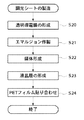
図2は、図1の調光体100の製造処理のフローチャートである。
【0036】
図2において、まず、厚みが175μmであるPETフィルム105a,bの各々において、その片面上にITO膜からなる透明導電膜106a,bを形成する(ステップS20)。
【0037】
次いで、液晶材料と水性相とを混合してエマルジョンを作製し、該作製されたエマルジョンをラテックスに添加するか、又は、液晶材料とラテックスを直接混合してエマルジョンを作製する。このとき、安定した液晶粒子を形成するために、エマルジョンに界面活性剤を添加することが好ましい。また、液晶材料と水性相又はラテックスとの混合は、ブレンダー、コロイドミル等のミキサーを行う(ステップS21)。このミキサーの回転数によって液晶カプセル103のカプセル径(D1)を所望の値に制御することができ、このとき、当該D1は約5μmに制御される。
【0038】
さらに、作製されたエマルジョン中のラテックスを架橋するため架橋剤を添加して媒体を形成する(ステップS22)。当該架橋剤の分量は、ラテックスの固形分量に対応して、この固形分量相当のラテックスの全てを架橋可能な分量に設定される。
【0039】
そして、形成された媒体をナイフブレード又は他の適当な手段によって透明導電膜106a上に塗布し、塗布された媒体を乾燥させることによって架橋剤によるラテックスの架橋を進行させて液晶層104を形成する(ステップS23)。
【0040】
次いで、形成された液晶層104に透明導電膜106bが接するようにPETフィルム105bを貼り合わせ(ステップS24)、本処理を終了する。
【0041】
また、調光体100では、Δnが低いと電圧印加時のヘイズは低減されるという液晶材料の性質を利用して、ネマティック液晶の棒状分子102のΔnは小さく設定される。具体的には、△nが0.12より大きいと十分に低いヘイズが得られない一方、△nが小さすぎると電圧無印加時の遮蔽性が低下するため、ネマティック液晶の棒状分子102の△nは0.08≦Δn≦0.12に設定される。
【0042】
さらに、液晶カプセル103のカプセル径(D1)については、カプセル径(D1)が小さすぎるとカプセル径の小径化に伴う散乱量の増加により可視域での平均透過率は低くなるものの、長波長側の光が液晶カプセル103を回折することによりビジビリティー(V)が高くなり、結局、電圧無印加時の遮蔽性が低下する一方、カプセル径(D1)が大きすぎるとカプセル径の大径化に伴う散乱量の低下によりビジビリティー(V)が高くなり、やはり電圧無印加時の遮蔽性が低下する。従って、調光体100では、△nとカプセル径(D1)との積△n*D1が0.55≧D1*△n≧0.45の範囲に設定される。
【0043】
ここで、△nが一定であるとすると、0.45>D1*△の範囲ではカプセル径が小さいことを示し、△n*D1>0.55の範囲ではカプセル径が大きいことを示す。
【0044】
一般に、ビジビリティー(V)を低くして遮蔽性を向上させるには、液晶層104の膜厚を厚くするのが効果的であるが、単純に液晶層104の膜厚を厚くするだけでは、電圧印加時のヘイズが高くなり、調光体100に必要とされる性能を達成できない。
【0045】
また、液晶材料では、大きなカプセル径を有する液晶カプセル103の割合が増加すると、透過光が可視域でほとんど散乱しなくなるため、ビジビリティー(V)が高くなり、電圧無印加時の遮蔽性が低下する。この場合、単純に、カプセル径(D1)を小さくすることによりビジビリティー(V)を低くし、遮蔽性を向上させることができるが、やはり電圧印加時のヘイズが高くなり、必要とされる調光体の性能は得られない。
【0046】
従って、調光体100では、カプセル径(D1)とカプセル径分布(D3/D2)が2.5*D1≧D3/D2の関係を満たすように設定される。
【0047】
以上より、本実施の形態に係る調光体100では、ネマティック液晶の棒状分子102の△nが0.08≦Δn≦0.12に設定され、△nとカプセル径(D1)との積△n*D1が0.55≧D1*△n≧0.45の範囲に設定され、且つカプセル径(D1)とカプセル径分布(D3/D2)が2.5*D1≧D3/D2の関係を満たすように設定されるので、電圧印加時のヘイズの視野角依存性を低減できると共に、電圧無印加時の高遮蔽性、電圧印加時の低電圧駆動、及び電圧印加時の低ヘイズ化を実現できる。
【0048】
本実施の形態に係る調光体100における液晶は、ネマティック液晶の棒状分子102に限定されるものではなく、コレステリック液晶及びスメクティック液晶を用いてもよい。
【0049】
本実施の形態に係る調光体100におけるポリマーフィルム101は、その屈折率nとネマティック液晶等の液晶材料の常光線屈折率noとが一致する材料であって、液晶材料を複数のカプセル状に保持できるものであればよく、無機及び有機の種類を問わずに用いることができるが、特に、PETフィルム105上に形成された透明導電膜106との接着性、及び光学的均一性を有するラテックスが好ましく、これにより物理的耐久性に優れた調光体100を提供することができる。
【0050】
また、本実施の形態に係る調光体100における透明導電膜106が形成されたPETフィルム105の代わりに、インジウム鉱酸化物(ITO)膜や錫酸化物(SnO2)膜が表面に形成されたガラス板やプラスチックフィルム等を用いてもよい。
【0051】
【実施例】
次に、本発明に係る実施例を具体的に説明する。
【0052】
液晶ZLI−4171(メルク社製、△n=0.097)に界面活性剤IGEPAL CO−610(GAF社製)を0.5wt%添加し、該界面活性剤が添加された液晶を液晶比率が0.62になるようにラテックス粒子40重量%を含むNeorez R―967(ゼネカ社製)に添加した後、ホモジナイザーを用い7000回転で10分間撹拌してエマルジョンを得た。次いて、該エマルジョンをゆっくり混ぜながら架橋剤CX−100(ゼネカ社製)をエマルジョンに対して3重量%の割合で添加した。そして、架橋剤が添加されたエマルジョンをドクターブレードを用いて、ITO膜付きPETフィルム上に塗布し、乾燥した。
【0053】
そして、塗布されたエマルジョンの乾燥後、該エマルジョンをもう一枚のITO膜付きPETフィルムと貼合わせ、調光体を得た。当該調光体の厚みは20μmであった。
【0054】
また、上記調光体では、液晶カプセルのカプセル径(D1)は5μmであり、カプセル径分布(D3/D2)は11.5であった。
【0055】
このようにして得られた調光体のビジビリティーを瞬間マルチ測光システムMCPD−1000(28C)(大塚電子株式会社製)を用いて測定し、サイン波/100V/50Hzである低電圧を印加したヘイズをヘーズメータによって測定した結果、測定結果は、ビジビリティー(V)=0.08、ヘイズ=8%であり、電圧無印加時の高遮蔽性を確保しつつ、電圧印加時の低ヘイズ化を実現できることが分かった。
【0056】
従って、調光体において△nが0.08≦Δn≦0.12であり、△nとカプセル径(D1)との積△n*D1が0.55≧D1*△n≧0.45であり、且つカプセル径(D1)とカプセル径分布(D3/D2)が2.5*D1≧D3/D2であれば、当該調光体は十分な視野制御性能を有し、電圧無印加時の高遮蔽性、電圧印加時の低電圧駆動、及び電圧印加時の低ヘイズ化を実現できることが分かった。
【0057】
【発明の効果】
以上、詳細に説明したように、請求項1記載の調光体によれば、液晶材料の複屈折率(△n)が0.12≧△n≧0.08の範囲にあり、空孔の体積と同体積の真球体における平均直径D1及び複屈折率Δnの積が0.55μm≧D1*△n≧0.45μmの範囲にあり、空孔の真球換算直径の積算分布において、換算直径小側からの積算割合が10%である領域における最大直径D2と、換算直径小側からの積算割合が90%である領域における最大直径D3との比が2.5*D1≧D3/D2であるので、電圧印加時のヘイズの視野角依存性を低減できると共に、電圧無印加時の高遮蔽性、電圧印加時の低電圧駆動、及び電圧印加時の低ヘイズ化を実現できる。
【図面の簡単な説明】
【図1】本発明の実施の形態に係る調光体の断面図である。
【図2】図1の調光体100の製造処理のフローチャートである。
【符号の説明】
100 調光体
101 ポリマーフィルム
102 ネマティック液晶
103 液晶カプセル
104 液晶層
105 PETフィルム
106 透明導電膜[0001]
TECHNICAL FIELD OF THE INVENTION
The present invention relates to a dimmer having a liquid crystal material and a laminated glass including the dimmer, and more particularly to a dimmer capable of controlling a visual field and a laminated glass including the dimmer.
[0002]
[Prior art]
2. Description of the Related Art Conventionally, an electrochromic device (hereinafter, referred to as an “EC device”) has been known as a device having a dimming function of arbitrarily adjusting the transmittance of a dimmer or the like (hereinafter, referred to as a “dimming device”). This EC element is made of a material such as tungsten oxide, Prussian blue, etc., which undergoes a spectrum change due to an electrochemical oxidation-reduction reaction, and controls the amount of transmitted light by absorbing light. Because it is a drive type, when the area is increased, a large voltage drop occurs and the response speed is remarkably reduced, and degradation occurs due to electrochemical changes in the constituent materials that occur during long-time energization. Cannot be applied to a light control body that requires
[0003]
Therefore, in recent years, a voltage-driven dimming element has been applied to laminated glass instead of the above-described current-driven EC element. For example, a nematic (NCAP: Nematic Curviliner Aligned Phase) liquid crystal light modulator having a curvilinear array phase is known as such a voltage-driven light control element. The nematic liquid crystal light controller is made of a liquid crystal material. It is configured, has excellent durability, and is easy to increase in area (for example, Patent Document 1).
[0004]
Usually, such a dimmer includes a liquid crystal layer having a dimming function in which liquid crystal is sealed in a plurality of holes, and a pair of PET films sandwiching the liquid crystal layer therebetween. A voltage is applied to the liquid crystal layer through the pair of transparent conductive films, which are disposed on opposite surfaces of each PET film so as to adhere to the layers. The liquid crystal layer is formed of a transparent polymer film having a large number of holes, and each of the holes forms a liquid crystal capsule by being filled with liquid crystal.
[0005]
In this dimmer, when no voltage is applied, the liquid crystal molecules are aligned along the curved surface of the wall of the liquid crystal capsule and are not arranged along the traveling direction of the transmitted light passing through the liquid crystal capsule, so that the optical path of the transmitted light is bent. Or the liquid crystal layer becomes milky by scattering incident light at the boundary layer between the liquid crystal capsule and the polymer film. On the other hand, in this dimmer, when a voltage is applied, the liquid crystal molecules are aligned along the direction of the generated electric field. At this time, a material such that the refractive index np of the polymer film and the ordinary refractive index no of the liquid crystal molecules match. By forming the liquid crystal layer from the above, the boundary layer between the liquid crystal capsule and the polymer film is not optically present, and the transmitted light incident on the liquid crystal layer can be transmitted as it is, thereby making the liquid crystal layer transparent.
[0006]
Based on the principle described above, the dimmer controls the visual field by scattering incident light when no voltage is applied, and secures the visual field by transmitting incident light as it is when voltage is applied. Has functions.
[0007]
The dimmer is preferably used alone or in the form of a laminated glass sandwiched between a plurality of plate glasses for a partition or the like by the above-mentioned view control function.
[0008]
Here, the scattering degree that slightly remains in the transparent state is referred to as haze. In the above-described light control body, the light-shielding property when no voltage is applied, the low voltage driving when applying a voltage, and the low light level when applying a voltage are used. Haze is required. Furthermore, when the light control body is used for a window glass of a building or a window glass of an automobile, since these window glasses have a large opening area, the haze at the time of voltage application is reduced, and the viewing angle dependence of haze is small. Is required.
[0009]
It is known that the use of a liquid crystal having a low birefringence (hereinafter referred to as “Δn”) can reduce the viewing angle dependency of haze when a voltage is applied by a sine wave power supply (for example, Patent Document 2). .
[0010]
[Patent Document 1]
JP-T-58-501631 [Patent Document 2]
Japanese Patent Application Laid-Open No. H3-116019
[Problems to be solved by the invention]
By using a liquid crystal having a low Δn as described above, the viewing angle dependency of the haze when a voltage is applied is improved, but the shielding property when no voltage is applied tends to decrease. At this time, it is necessary to increase the film thickness (the thickness of the liquid crystal layer) in order to compensate for a decrease in the shielding property when no voltage is applied. However, when the film thickness is increased, there is a problem that the haze at the time of applying a voltage and the driving voltage increase.
[0012]
The present invention provides a dimmer capable of reducing the viewing angle dependence of haze when a voltage is applied, realizing high shielding when no voltage is applied, low voltage driving when a voltage is applied, and low haze when a voltage is applied. And to provide a laminated glass.
[0013]
[Means for Solving the Problems]
In order to achieve the above object, the dimmer according to claim 1 has a plurality of holes, and the liquid crystal layer is sandwiched between a liquid crystal layer in which a liquid crystal material is sealed in each of the holes. In a dimmer including at least one pair of transparent substrates and a transparent conductive film disposed on the opposing surface of each of the substrates, a birefringence △ n of the liquid crystal material is 0.12 ≧ 2n ≧ 0.08, wherein the product of the average diameter D1 and the birefringence Δn in a true sphere having the same volume as the hole is in the range of 0.55 μm ≧ D1 * △ n ≧ 0.45 μm, In the integrated distribution of the true sphere converted diameters, the maximum diameter D2 in a region where the integrated ratio from the small converted diameter side is 10% and the maximum diameter D3 in a region where the integrated ratio from the small converted diameter side is 90%. The ratio is 2.5 * D1 ≧ D3 / D2.
[0014]
According to the dimmer of the first aspect, the birefringence (Δn) of the liquid crystal material is in the range of 0.12 ≧ Δn ≧ 0.08, and the average in a true sphere having the same volume as the volume of the pores. The product of the diameter D1 and the birefringence index Δn is in the range of 0.55 μm ≧ D1 * △ n ≧ 0.45 μm, and in the integrated distribution of the sphere converted diameters of the pores, the integration ratio from the small converted diameter side is 10%. Since the ratio of the maximum diameter D2 in the region where is the ratio to the maximum diameter D3 in the region where the integration ratio from the reduced diameter side is 90% is 2.5 * D1 ≧ D3 / D2, the haze at the time of voltage application is The viewing angle dependency can be reduced, and high shielding performance when no voltage is applied, low voltage driving when voltage is applied, and low haze when voltage is applied can be realized.
[0015]
A laminated glass according to a second aspect is provided with the dimmer according to the first aspect.
[0016]
According to the laminated glass of claim 2, the viewing angle dependence of the haze at the time of applying a voltage can be reduced, the high shielding property at the time of applying no voltage, the low-voltage driving at the time of applying a voltage, and the low haze at the time of applying a voltage. Can be realized.
[0017]
Hereinafter, in the integrated distribution of Δn of the liquid crystal, the average diameter D1 of a true sphere having the same volume as the hole (hereinafter referred to as “capsule diameter”), and the integrated distribution of the true sphere converted diameter of the same volume as the hole, For setting the ratio between the maximum diameter D2 in the region where the integration ratio from the area is 10% and the maximum diameter D3 in the region where the integration ratio from the reduced diameter side is 90% (hereinafter referred to as “capsule diameter distribution”) Will be described.
[0018]
In general, the practically required performance of a dimmer used for a window glass or the like is such that the visibility (V) showing a shielding property described later is 0.1 or less, and the haze upon application of a voltage is 10% or less. Here, the visibility (V) is an index that quantitatively represents the shielding property when no voltage is applied, and a light source, a screen, a dimmer having a liquid crystal, and a spectral luminance meter are sequentially arranged on the same optical axis. The luminance of white stripes (Iw) and the luminance of black stripes (lb) at a wavelength of 700 nm of a zebra pattern on a screen irradiated from a light source can be obtained from the following equation (1).
[0019]
Visibility (V) = (Iw-Ib) / (Iw + Ib) (1)
The haze can be measured by a haze meter (for example, “Suga Haze Meter” manufactured by Suga Test Instruments Co., Ltd.). Haze is a total transmittance (Tt) which is a ratio of the amount of transmitted light at all viewing angles to an amount of incident light, and a parallel transmittance (Tt) which is a ratio of the amount of transmitted light parallel to the incident light to the amount of incident light. Tp) can be obtained from the following equation (2).
[0020]
Haze = (Tt−Tp) / Tt (2)
Here, as described above, by using a liquid crystal having a low Δn, the haze at the time of voltage application is reduced, and when Δn is larger than 0.12, a sufficiently low haze cannot be obtained. On the other hand, when Δn is small, the shielding property when no voltage is applied is reduced. For example, when Δn is smaller than 0.08, even if the capsule diameter and the capsule diameter distribution are suitably combined, the visibility (V) becomes high, and a sufficiently high shielding property cannot be obtained. Therefore, Δn of the liquid crystal needs to be 0.08 or more and 0.12 or less.
[0021]
Further, there is a range of the capsule diameter (D1) and the capsule diameter distribution (D3 / D2) corresponding to the range of Δn of the liquid crystal and having the highest shielding property when no voltage is applied.
[0022]
First, regarding the capsule diameter, the product Δn * D1 of Δn and the capsule diameter (D1) needs to be within the range represented by the following equation (3).
[0023]
0.55 ≧ D1 * △ n ≧ 0.45 (3)
Here, assuming that Δn is constant, the capsule diameter is smaller in the range of 0.45> D1 * Δn than in the range of Expression (3). In this case, the average transmittance in the visible region decreases due to an increase in the amount of scattering due to the decrease in the capsule diameter, but the visibility (V) increases due to the diffraction of light on the long wavelength side, and after all, no voltage is applied. The shielding property at the time decreases.
[0024]
Further, the range of Δn * D1> 0.55 indicates that the capsule diameter is larger than the range of the expression (3). In this case, the visibility (V) is increased due to a decrease in the scattering amount due to an increase in the capsule diameter, and the shielding performance when no voltage is applied is also reduced.
[0025]
In any case, by increasing the film thickness, the visibility (V) when no voltage is applied can be lowered and the shielding property can be improved, but the haze at the time of voltage application becomes high, and the required dimming is required. Body performance is not obtained.
[0026]
Here, the required performance of the dimmer is satisfied when the capsule diameter (D1) and the capsule diameter distribution (D3 / D2) are represented by the following equation (4).
[0027]
2.5 * D1 ≧ D3 / D2 (4)
When the capsule diameter distribution (D3 / D2) is larger than 2.5 * D1, that is, when the capsule diameter distribution (D3 / D2) is wider than the range of the expression (4), the ratio of the large capsule diameter (D1) generally increases. However, since almost no scattering occurs in the visible region, the visibility (V) is increased, and the shielding property when no voltage is applied is reduced. In this case, by reducing the capsule diameter (D1) or increasing the film thickness, the visibility (V) can be lowered and the shielding property can be improved, but the haze at the time of applying a voltage is also increased, which is necessary. However, the performance of the dimmer cannot be obtained.
[0028]
As described above, in the present invention, despite the use of a liquid crystal substance having a low Δn, by suitably combining Δn, the capsule diameter (D1), and the capsule diameter distribution (D3 / D2) of the liquid crystal material, It is possible to drive at a low voltage when a voltage is applied without impairing the shielding property when no voltage is applied, and to realize a liquid crystal light modulator with a low haze.
[0029]
BEST MODE FOR CARRYING OUT THE INVENTION
Hereinafter, a dimmer according to an embodiment of the present invention will be described with reference to the drawings.
[0030]
FIG. 1 is a cross-sectional view of the dimmer according to the embodiment of the present invention.
[0031]
In FIG. 1, a dimmer 100 is composed of a transparent polymer film 101 made of latex having a plurality of pores, and a liquid crystal capsule 103 formed by enclosing rod-like molecules 102 of a nematic liquid crystal in each of the pores. , A pair of PET films 105a and 105b sandwiching the liquid crystal layer 104 therebetween, and transparent conductive films 106a and 106b disposed on opposing surfaces of the pair of PET films 105a and 105b, respectively. In the dimmer 100, the pair of transparent conductive films 106a and 106b apply a voltage to the liquid crystal layer 104.
[0032]
In the dimmer 100, when no voltage is applied to the liquid crystal layer 104, the rod-like molecules 102 of the nematic liquid crystal are aligned along the curved surface of the wall of the liquid crystal capsule 103, and along the traveling direction of the transmitted light passing through the liquid crystal capsule 103. Since the light is not aligned, the optical path of the transmitted light is bent or the incident light is scattered at the boundary layer between the liquid crystal capsule 103 and the polymer film 101 to make the liquid crystal layer 104 milky white. On the other hand, in the dimmer 100, when a voltage is applied to the liquid crystal layer 104, the nematic liquid crystal is aligned along the direction of the electric field in which the rod-shaped molecules 102 are generated. At this time, the refractive index np of the polymer film 101 and the nematic liquid crystal Since the liquid crystal layer 104 is made of a material in which the ordinary refractive index no of the rod-shaped molecule 102 matches, the boundary layer between the liquid crystal capsule 103 and the polymer film 101 is optically absent, and the light enters the liquid crystal layer 104. The transmitted light can be transmitted as it is, thereby making the liquid crystal layer 104 transparent.
[0033]
From the above principle, the dimmer 100 has a visual field control function of blocking the visual field by scattering incident light when no voltage is applied, and securing the visual field by transmitting the incident light as it is when a voltage is applied. Having.
[0034]
Next, a method for manufacturing the dimmer 100 will be described.
[0035]
FIG. 2 is a flowchart of a manufacturing process of the light control body 100 of FIG.
[0036]
In FIG. 2, first, for each of the PET films 105a and 105b having a thickness of 175 μm, transparent conductive films 106a and 106b made of an ITO film are formed on one surface thereof (step S20).
[0037]
Next, the liquid crystal material and the aqueous phase are mixed to prepare an emulsion, and the prepared emulsion is added to latex, or the liquid crystal material and the latex are directly mixed to prepare an emulsion. At this time, it is preferable to add a surfactant to the emulsion in order to form stable liquid crystal particles. The mixing of the liquid crystal material and the aqueous phase or latex is performed by a mixer such as a blender or a colloid mill (step S21). The capsule diameter (D1) of the liquid crystal capsule 103 can be controlled to a desired value by the rotation speed of the mixer. At this time, D1 is controlled to about 5 μm.
[0038]
Further, a crosslinking agent is added to crosslink the latex in the prepared emulsion to form a medium (Step S22). The amount of the crosslinking agent is set to an amount capable of crosslinking all of the latex corresponding to the solid content in accordance with the solid content of the latex.
[0039]
Then, the formed medium is applied on the transparent conductive film 106a by a knife blade or other appropriate means, and the applied medium is dried to progress the crosslinking of the latex by the crosslinking agent to form the liquid crystal layer 104. (Step S23).
[0040]
Next, the PET film 105b is attached so that the transparent conductive film 106b is in contact with the formed liquid crystal layer 104 (Step S24), and the present process ends.
[0041]
Further, in the dimmer 100, Δn of the rod-like molecule 102 of the nematic liquid crystal is set to be small by utilizing the property of the liquid crystal material that the haze upon application of a voltage is reduced when Δn is low. Specifically, when Δn is larger than 0.12, a sufficiently low haze cannot be obtained, while when Δn is too small, the shielding property when no voltage is applied is reduced. n is set to be 0.08 ≦ Δn ≦ 0.12.
[0042]
Further, regarding the capsule diameter (D1) of the liquid crystal capsule 103, if the capsule diameter (D1) is too small, the average transmittance in the visible region decreases due to an increase in the amount of scattering due to the reduction of the capsule diameter, but the long wavelength side The light (D) diffracts the liquid crystal capsule 103 to increase the visibility (V). As a result, the shielding property when no voltage is applied is reduced. On the other hand, if the capsule diameter (D1) is too large, the capsule diameter increases. The visibility (V) increases due to the decrease in the amount of scattering, and the shielding performance when no voltage is applied also decreases. Therefore, in the dimmer 100, the product Δn * D1 of Δn and the capsule diameter (D1) is set in a range of 0.55 ≧ D1 * Δn ≧ 0.45.
[0043]
Here, assuming that {n is constant, the range of 0.45> D1 *} indicates that the capsule diameter is small, and the range of {n * D1> 0.55 indicates that the capsule diameter is large.
[0044]
In general, it is effective to increase the film thickness of the liquid crystal layer 104 in order to lower the visibility (V) and improve the shielding property. However, simply increasing the film thickness of the liquid crystal layer 104 is not effective. The haze at the time of application becomes high, and the performance required for the light control body 100 cannot be achieved.
[0045]
In the liquid crystal material, when the ratio of the liquid crystal capsule 103 having a large capsule diameter increases, the transmitted light hardly scatters in the visible region, so that the visibility (V) increases and the shielding property when no voltage is applied decreases. . In this case, the visibility (V) can be lowered and the shielding property can be improved simply by reducing the capsule diameter (D1), but the haze at the time of applying a voltage is also increased, and the required dimming is required. Body performance is not obtained.
[0046]
Therefore, in the light control body 100, the capsule diameter (D1) and the capsule diameter distribution (D3 / D2) are set so as to satisfy the relationship of 2.5 * D1 ≧ D3 / D2.
[0047]
As described above, in the dimmer 100 according to the present embodiment, Δn of the rod-like molecule 102 of the nematic liquid crystal is set to 0.08 ≦ Δn ≦ 0.12, and the product of {n and the capsule diameter (D1)}. n * D1 is set in the range of 0.55 ≧ D1 * △ n ≧ 0.45, and the relationship between the capsule diameter (D1) and the capsule diameter distribution (D3 / D2) is 2.5 * D1 ≧ D3 / D2. Since the setting is made to satisfy, it is possible to reduce the viewing angle dependence of haze when applying voltage, realize high shielding performance when no voltage is applied, low voltage driving when applying voltage, and low haze when applying voltage it can.
[0048]
The liquid crystal in the dimmer 100 according to the present embodiment is not limited to the nematic liquid crystal rod-shaped molecules 102, but may be a cholesteric liquid crystal or a smectic liquid crystal.
[0049]
The polymer film 101 in the light modulating body 100 according to the present embodiment is a material in which the refractive index n matches the ordinary light refractive index no of a liquid crystal material such as a nematic liquid crystal, and the liquid crystal material is formed into a plurality of capsules. Any latex can be used as long as it can hold it, regardless of the type of inorganic or organic material. In particular, latex having adhesiveness to the transparent conductive film 106 formed on the PET film 105 and optical uniformity It is preferable to provide the light control body 100 having excellent physical durability.
[0050]
Also, instead of the PET film 105 on which the transparent conductive film 106 is formed in the light modulating body 100 according to the present embodiment, an indium oxide (ITO) film or a tin oxide (SnO 2 ) film is formed on the surface. A glass plate, a plastic film, or the like may be used.
[0051]
【Example】
Next, examples according to the present invention will be specifically described.
[0052]
0.5 wt% of a surfactant IGEPAL CO-610 (manufactured by GAF) is added to a liquid crystal ZLI-4171 (manufactured by Merck, Δn = 0.097), and the liquid crystal having the surfactant added has a liquid crystal ratio of 0.5% by weight. After adding to Neorez R-967 (manufactured by Zeneca) containing 40% by weight of latex particles so as to be 0.62, the mixture was stirred at 7000 rpm for 10 minutes using a homogenizer to obtain an emulsion. Next, a crosslinking agent CX-100 (manufactured by Zeneca) was added at a ratio of 3% by weight to the emulsion while slowly mixing the emulsion. Then, the emulsion to which the crosslinking agent was added was applied on a PET film with an ITO film using a doctor blade, and dried.
[0053]
After drying the applied emulsion, the emulsion was bonded to another PET film with an ITO film to obtain a light control body. The thickness of the light control body was 20 μm.
[0054]
In the dimmer, the capsule diameter (D1) of the liquid crystal capsule was 5 μm, and the capsule diameter distribution (D3 / D2) was 11.5.
[0055]
The visibility of the dimmer obtained in this manner was measured using an instantaneous multi-photometry system MCPD-1000 (28C) (manufactured by Otsuka Electronics Co., Ltd.), and a haze to which a low voltage of sine wave / 100 V / 50 Hz was applied. Was measured with a haze meter, and the result was that the visibility (V) was 0.08 and the haze was 8%, and it was possible to realize a low haze at the time of applying a voltage while securing a high shielding property when no voltage was applied. I understood.
[0056]
Therefore, in the dimmer, Δn is 0.08 ≦ Δn ≦ 0.12, and the product Δn * D1 of Δn and the capsule diameter (D1) is 0.55 ≧ D1 * Δn ≧ 0.45. If the capsule diameter (D1) and the capsule diameter distribution (D3 / D2) are 2.5 * D1 ≧ D3 / D2, the dimmer has sufficient visual field control performance, It was found that high shielding properties, low voltage driving at the time of applying a voltage, and low haze at the time of applying a voltage can be realized.
[0057]
【The invention's effect】
As described above in detail, according to the dimmer of the first aspect, the birefringence (Δn) of the liquid crystal material is in the range of 0.12 ≧ Δn ≧ 0.08, The product of the average diameter D1 and the birefringence index Δn of a true sphere having the same volume as the volume is in the range of 0.55 μm ≧ D1 * △ n ≧ 0.45 μm, The ratio of the maximum diameter D2 in the region where the integration ratio from the small side is 10% to the maximum diameter D3 in the region where the integration ratio from the reduced diameter side is 90% is 2.5 * D1 ≧ D3 / D2. Therefore, the dependence of the haze upon application of a voltage to the viewing angle can be reduced, and high shielding properties when no voltage is applied, low voltage driving when applying a voltage, and low haze when applying a voltage can be realized.
[Brief description of the drawings]
FIG. 1 is a sectional view of a dimmer according to an embodiment of the present invention.
FIG. 2 is a flowchart of a manufacturing process of the light control body 100 of FIG.
[Explanation of symbols]
REFERENCE SIGNS LIST 100 dimmer 101 polymer film 102 nematic liquid crystal 103 liquid crystal capsule 104 liquid crystal layer 105 PET film 106 transparent conductive film