JP2004303399A - フラッシュメモリセルのプログラム方法及びこれを用いたnand型フラッシュメモリのプログラム方法 - Google Patents
フラッシュメモリセルのプログラム方法及びこれを用いたnand型フラッシュメモリのプログラム方法 Download PDFInfo
- Publication number
- JP2004303399A JP2004303399A JP2004041554A JP2004041554A JP2004303399A JP 2004303399 A JP2004303399 A JP 2004303399A JP 2004041554 A JP2004041554 A JP 2004041554A JP 2004041554 A JP2004041554 A JP 2004041554A JP 2004303399 A JP2004303399 A JP 2004303399A
- Authority
- JP
- Japan
- Prior art keywords
- flash memory
- memory cell
- over
- voltage
- programming
- Prior art date
- Legal status (The legal status is an assumption and is not a legal conclusion. Google has not performed a legal analysis and makes no representation as to the accuracy of the status listed.)
- Granted
Links
- 238000000034 method Methods 0.000 title claims abstract description 39
- 238000011084 recovery Methods 0.000 claims abstract description 38
- 238000012790 confirmation Methods 0.000 claims 1
- 230000007547 defect Effects 0.000 abstract description 3
- 238000010586 diagram Methods 0.000 description 5
- 230000005684 electric field Effects 0.000 description 4
- 239000004065 semiconductor Substances 0.000 description 4
- 239000000758 substrate Substances 0.000 description 3
- 239000000969 carrier Substances 0.000 description 2
- 101100049574 Human herpesvirus 6A (strain Uganda-1102) U5 gene Proteins 0.000 description 1
- 238000007796 conventional method Methods 0.000 description 1
- 230000008878 coupling Effects 0.000 description 1
- 238000010168 coupling process Methods 0.000 description 1
- 238000005859 coupling reaction Methods 0.000 description 1
- 101150013423 dsl-1 gene Proteins 0.000 description 1
- 238000012986 modification Methods 0.000 description 1
- 230000004048 modification Effects 0.000 description 1
- 101150064834 ssl1 gene Proteins 0.000 description 1
- 230000005641 tunneling Effects 0.000 description 1
Images


Classifications
-
- G—PHYSICS
- G11—INFORMATION STORAGE
- G11C—STATIC STORES
- G11C16/00—Erasable programmable read-only memories
- G11C16/02—Erasable programmable read-only memories electrically programmable
- G11C16/06—Auxiliary circuits, e.g. for writing into memory
- G11C16/34—Determination of programming status, e.g. threshold voltage, overprogramming or underprogramming, retention
- G11C16/3404—Convergence or correction of memory cell threshold voltages; Repair or recovery of overerased or overprogrammed cells
-
- G—PHYSICS
- G11—INFORMATION STORAGE
- G11C—STATIC STORES
- G11C16/00—Erasable programmable read-only memories
- G11C16/02—Erasable programmable read-only memories electrically programmable
- G11C16/06—Auxiliary circuits, e.g. for writing into memory
- G11C16/34—Determination of programming status, e.g. threshold voltage, overprogramming or underprogramming, retention
- G11C16/3436—Arrangements for verifying correct programming or erasure
- G11C16/3454—Arrangements for verifying correct programming or for detecting overprogrammed cells
Landscapes
- Read Only Memory (AREA)
Abstract
オーバプログラムに起因する読出し欠陥を改善することができ、セルのプログラム時にしきい値電圧ターゲットを自由に設定することができ、マルチレベルセルのプログラム方法としても使用可能なフラッシュメモリセルのプログラム方法及びこれを用いたNAND型フラッシュメモリのプログラム方法を提供する。
【解決手段】
プログラムすべきフラッシュメモリセルをオーバプログラムする段階と、前記フラッシュメモリセルのゲートバイアスを調節し、オーバプログラムされたフラッシュメモリセルをリカバリする第1リカバリ段階と、前記ゲートバイアスを0Vの電圧にセットした後、オーバプログラムされたフラッシュメモリセルのバルクバイアスを調節してリカバリする第2リカバリ段階と、前記ゲートバイアスをフローティングさせた後、オーバプログラムされたフラッシュメモリセルのバルクバイアスを調節してリカバリする第3リカバリ段階と、セルフブースティング動作を用いて、オーバプログラムされたフラッシュメモリセルのバルクバイアスを調節してリカバリする第4リカバリ段階とを含んでなる。
【選択図】図5
Description

選択されたワードラインW/Lには20V以上の電圧を印加し、ドレイン選択ラインDSLには電源電圧Vccを印加する。そして、選択されたビットラインB/L、ソース選択ラインSSL及びバルク領域には、ゼロ (zero) 電圧を維持させる。
選択されたワードラインには8V以上の電圧、ドレイン選択ラインにはVcc電圧、ソース選択ラインには0Vの電圧をそれぞれ印加し、ビットライン及びバルクはフローティングさせる一方、ソースには0Vの電圧を印加する。
選択されたワードラインには0V以上の電圧、ドレイン選択ラインにはVcc電圧、ソース選択ラインには0Vの電圧をそれぞれ印加し、ビットラインはフローティングさせる一方、ソースには0Vの電圧、バルクには12〜13Vの電圧をそれぞれ印加する。
選択されたワードラインはフローティングさせ、ドレイン選択ラインにはVcc電圧、ソース選択ラインには0Vの電圧をそれぞれ印加し、ビットラインはフローティングさせる一方、ソースには0Vの電圧、バルクには8Vの電圧をそれぞれ印加する。
選択されたワードラインには0Vの電圧、ドレイン選択ラインにはVcc電圧、ソース選択ラインには0Vの電圧をそれぞれ印加し、ビットラインは12+Vtn電圧を印加する一方、ソース及びバルクには0Vの電圧を印加する。
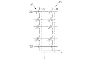
st2 … 第2ストリング
c1〜c16 … 第1〜第16メモリセル
Claims (7)
- プログラムすべきフラッシュメモリセルをオーバプログラムする段階と、
前記フラッシュメモリセルのゲートバイアスを調節することによって、オーバプログラムされたフラッシュメモリセルをリカバリする第1リカバリ段階と、
前記ゲートバイアスを0Vの電圧にセットした後、オーバプログラムされたフラッシュメモリセルのバルクバイアスを調節してリカバリする第2リカバリ段階と、
前記ゲートバイアスをフローティングさせた後、オーバプログラムされたフラッシュメモリセルのバルクバイアスを調節してリカバリする第3リカバリ段階と、
セルフブースティング動作を用いて、オーバプログラムされたフラッシュメモリセルのバルクバイアスを調節してリカバリする第4リカバリ段階と
を含んでなるフラッシュメモリセルのプログラム方法。 - 請求項1に記載のフラッシュメモリセルのプログラム方法において、
前記オーバプログラムする段階の間、前記フラッシュメモリセルのゲートに約20Vの電圧が印加される
ことを特徴とする方法。 - 請求項1に記載のフラッシュメモリセルのプログラム方法において、
前記第1リカバリ段階の間、前記フラッシュメモリセルのゲートに約8Vの電圧が印加される
ことを特徴とする方法。 - 請求項1に記載のフラッシュメモリセルのプログラム方法において、
前記第2リカバリ段階の間、前記フラッシュメモリセルのゲートが接地され、バルクに約12〜13Vの電圧が印加される
ことを特徴とする方法。 - 請求項1に記載のフラッシュメモリセルのプログラム方法において、
前記第3リカバリ段階の間、前記フラッシュメモリセルのゲートがフローティングされ、バルクに8Vの電圧が印加される
ことを特徴とする方法。 - 請求項1に記載のフラッシュメモリセルのプログラム方法において、
前記第4リカバリ段階の間、前記フラッシュメモリセルのゲートに0Vの電圧が印加され、ドレインに約12V+Vtnの電圧が印加される
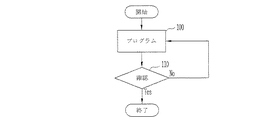
ことを特徴とする方法。 - 選択されたワードライン(W/L)に連結された全てのフラッシュメモリセルをオーバプログラムする段階と、
前記ワードラインに印加されるゲートバイアスを調節し、オーバプログラムされたフラッシュメモリセルをリカバリする第1リカバリ段階と、
前記ワードラインに印加されるゲートバイアスを0Vの電圧にセットした後、オーバプログラムされたフラッシュメモリセルのバルクバイアスを調節してリカバリする第2リカバリ段階と、
前記ワードラインをフローティングさせた後、オーバプログラムされたフラッシュメモリセルのバルクバイアスを調節してリカバリする第3リカバリ段階と、
セルフブースティング動作を用いて、オーバプログラムされたフラッシュメモリセルのバルクバイアスを調節してリカバリする第4リカバリ段階と、
プログラムが正常的に行われたか否かを確認する段階と、
前記確認段階の結果に応じて、前記第1リカバリ段階に復帰し、あるいは前記第1〜第4リカバリ段階の各バイアスを増加させた後、前記第1リカバリ段階に復帰する段階と
を含んでなるNAND型フラッシュメモリのプログラム方法。
Applications Claiming Priority (1)
| Application Number | Priority Date | Filing Date | Title |
|---|---|---|---|
| KR10-2003-0019990A KR100525910B1 (ko) | 2003-03-31 | 2003-03-31 | 플래시 메모리 셀의 프로그램 방법 및 이를 이용한 낸드플래시 메모리의 프로그램 방법 |
Publications (2)
| Publication Number | Publication Date |
|---|---|
| JP2004303399A true JP2004303399A (ja) | 2004-10-28 |
| JP4355588B2 JP4355588B2 (ja) | 2009-11-04 |
Family
ID=32985914
Family Applications (1)
| Application Number | Title | Priority Date | Filing Date |
|---|---|---|---|
| JP2004041554A Expired - Fee Related JP4355588B2 (ja) | 2003-03-31 | 2004-02-18 | Nand型フラッシュメモリのプログラム方法 |
Country Status (4)
| Country | Link |
|---|---|
| US (1) | US6999343B2 (ja) |
| JP (1) | JP4355588B2 (ja) |
| KR (1) | KR100525910B1 (ja) |
| TW (1) | TWI265520B (ja) |
Cited By (2)
| Publication number | Priority date | Publication date | Assignee | Title |
|---|---|---|---|---|
| JP2010225225A (ja) * | 2009-03-23 | 2010-10-07 | Toshiba Corp | Nand型フラッシュメモリ |
| JP2011100533A (ja) * | 2009-11-05 | 2011-05-19 | Fs Semiconductor Corp Ltd | フラッシュepromの閾値電圧降下方法及びその構造 |
Families Citing this family (11)
| Publication number | Priority date | Publication date | Assignee | Title |
|---|---|---|---|---|
| US7072217B2 (en) * | 2004-02-24 | 2006-07-04 | Micron Technology, Inc. | Multi-state memory cell with asymmetric charge trapping |
| US7428610B2 (en) * | 2006-02-14 | 2008-09-23 | Atmel Corporation | Writing to flash memory |
| KR100764053B1 (ko) * | 2006-08-10 | 2007-10-08 | 삼성전자주식회사 | 플래시 메모리 장치 및 그것의 프로그램 방법 |
| US7630249B2 (en) * | 2007-06-21 | 2009-12-08 | Sandisk Corporation | Intelligent control of program pulse duration |
| EP2160735A4 (en) * | 2007-06-21 | 2011-04-20 | Sandisk Corp | INTELLIGENT CONTROL OF THE PROGRAM IMPULSE DURATION |
| US7580290B2 (en) * | 2007-06-21 | 2009-08-25 | Sandisk Corporation | Non-volatile storage system with intelligent control of program pulse duration |
| KR101274205B1 (ko) * | 2007-07-13 | 2013-06-14 | 삼성전자주식회사 | 비휘발성 메모리 소자의 동작 방법 |
| US7978520B2 (en) | 2007-09-27 | 2011-07-12 | Sandisk Corporation | Compensation of non-volatile memory chip non-idealities by program pulse adjustment |
| US8014209B2 (en) | 2008-07-02 | 2011-09-06 | Sandisk Technologies Inc. | Programming and selectively erasing non-volatile storage |
| KR101200128B1 (ko) * | 2010-12-24 | 2012-11-12 | 에스케이하이닉스 주식회사 | 불휘발성 메모리 장치 및 그 프로그램 방법 |
| JP2020009511A (ja) * | 2018-07-05 | 2020-01-16 | キオクシア株式会社 | メモリシステム及び不揮発性半導体メモリ |
Family Cites Families (1)
| Publication number | Priority date | Publication date | Assignee | Title |
|---|---|---|---|---|
| US6775184B1 (en) * | 2003-01-21 | 2004-08-10 | Nexflash Technologies, Inc. | Nonvolatile memory integrated circuit having volatile utility and buffer memories, and method of operation thereof |
-
2003
- 2003-03-31 KR KR10-2003-0019990A patent/KR100525910B1/ko not_active Expired - Fee Related
- 2003-12-17 US US10/738,235 patent/US6999343B2/en not_active Expired - Lifetime
- 2003-12-18 TW TW092135982A patent/TWI265520B/zh not_active IP Right Cessation
-
2004
- 2004-02-18 JP JP2004041554A patent/JP4355588B2/ja not_active Expired - Fee Related
Cited By (3)
| Publication number | Priority date | Publication date | Assignee | Title |
|---|---|---|---|---|
| JP2010225225A (ja) * | 2009-03-23 | 2010-10-07 | Toshiba Corp | Nand型フラッシュメモリ |
| US8179720B2 (en) | 2009-03-23 | 2012-05-15 | Kabushiki Kaisha Toshiba | NAND flash memory |
| JP2011100533A (ja) * | 2009-11-05 | 2011-05-19 | Fs Semiconductor Corp Ltd | フラッシュepromの閾値電圧降下方法及びその構造 |
Also Published As
| Publication number | Publication date |
|---|---|
| KR100525910B1 (ko) | 2005-11-02 |
| TW200428396A (en) | 2004-12-16 |
| US6999343B2 (en) | 2006-02-14 |
| US20040190354A1 (en) | 2004-09-30 |
| KR20040085342A (ko) | 2004-10-08 |
| TWI265520B (en) | 2006-11-01 |
| JP4355588B2 (ja) | 2009-11-04 |
Similar Documents
| Publication | Publication Date | Title |
|---|---|---|
| US20240412782A1 (en) | Semiconductor memory device | |
| US8406052B2 (en) | High voltage generation and control in source-side injection programming of non-volatile memory | |
| US7796433B2 (en) | Apparatus for reducing the impact of program disturb | |
| KR100824203B1 (ko) | 플래시 메모리 소자의 프로그램 방법 | |
| US20080158998A1 (en) | Flash memory device capable of preventing an overerase of flash memory cells and erase method thereof | |
| CN102760483B (zh) | 半导体装置的操作方法 | |
| US20080158991A1 (en) | Systems for programming non-volatile memory with reduced program disturb by using different pre-charge enable voltages | |
| US7646639B2 (en) | Circuit and method generating program voltage for non-volatile memory device | |
| CN106531219A (zh) | 存储器装置 | |
| US20120092931A1 (en) | Nonvolatile semiconductor memory device | |
| CN101558450A (zh) | 用于对非易失性存储器单元进行低电压编程的方法及系统 | |
| JP4355588B2 (ja) | Nand型フラッシュメモリのプログラム方法 | |
| US20070242524A1 (en) | Reducing the impact of program disturb | |
| US9779830B2 (en) | Non-volatile semiconductor memory device and erase method thereof | |
| US7366020B2 (en) | Flash memory device capable of preventing an overerase of flash memory cells and erase method thereof | |
| US20070242510A1 (en) | Reducing the impact of program disturb during read | |
| US6914827B2 (en) | Flash memory device capable of preventing an over-erase of flash memory cells and erase method thereof | |
| US20070242509A1 (en) | Apparatus for reducing the impact of program disturb during read | |
| KR100589469B1 (ko) | 단시간에 소거 동작을 행하는 비휘발성 메모리 | |
| JP4988264B2 (ja) | ワードライン電圧の勾配を制御する不揮発性メモリ装置及びそのプログラム方法 | |
| WO2008079725A2 (en) | Method and system of low voltage programming of non-volatile memory cells |
Legal Events
| Date | Code | Title | Description |
|---|---|---|---|
| A621 | Written request for application examination |
Free format text: JAPANESE INTERMEDIATE CODE: A621 Effective date: 20060914 |
|
| A977 | Report on retrieval |
Free format text: JAPANESE INTERMEDIATE CODE: A971007 Effective date: 20090311 |
|
| A131 | Notification of reasons for refusal |
Free format text: JAPANESE INTERMEDIATE CODE: A131 Effective date: 20090331 |
|
| A521 | Written amendment |
Free format text: JAPANESE INTERMEDIATE CODE: A523 Effective date: 20090625 |
|
| TRDD | Decision of grant or rejection written | ||
| A01 | Written decision to grant a patent or to grant a registration (utility model) |
Free format text: JAPANESE INTERMEDIATE CODE: A01 Effective date: 20090721 |
|
| A01 | Written decision to grant a patent or to grant a registration (utility model) |
Free format text: JAPANESE INTERMEDIATE CODE: A01 |
|
| A61 | First payment of annual fees (during grant procedure) |
Free format text: JAPANESE INTERMEDIATE CODE: A61 Effective date: 20090803 |
|
| R150 | Certificate of patent or registration of utility model |
Free format text: JAPANESE INTERMEDIATE CODE: R150 |
|
| FPAY | Renewal fee payment (event date is renewal date of database) |
Free format text: PAYMENT UNTIL: 20120807 Year of fee payment: 3 |
|
| FPAY | Renewal fee payment (event date is renewal date of database) |
Free format text: PAYMENT UNTIL: 20120807 Year of fee payment: 3 |
|
| S531 | Written request for registration of change of domicile |
Free format text: JAPANESE INTERMEDIATE CODE: R313531 |
|
| FPAY | Renewal fee payment (event date is renewal date of database) |
Free format text: PAYMENT UNTIL: 20120807 Year of fee payment: 3 |
|
| R360 | Written notification for declining of transfer of rights |
Free format text: JAPANESE INTERMEDIATE CODE: R360 |
|
| FPAY | Renewal fee payment (event date is renewal date of database) |
Free format text: PAYMENT UNTIL: 20120807 Year of fee payment: 3 |
|
| R370 | Written measure of declining of transfer procedure |
Free format text: JAPANESE INTERMEDIATE CODE: R370 |
|
| FPAY | Renewal fee payment (event date is renewal date of database) |
Free format text: PAYMENT UNTIL: 20130807 Year of fee payment: 4 |
|
| R250 | Receipt of annual fees |
Free format text: JAPANESE INTERMEDIATE CODE: R250 |
|
| S111 | Request for change of ownership or part of ownership |
Free format text: JAPANESE INTERMEDIATE CODE: R313113 |
|
| S531 | Written request for registration of change of domicile |
Free format text: JAPANESE INTERMEDIATE CODE: R313531 |
|
| S533 | Written request for registration of change of name |
Free format text: JAPANESE INTERMEDIATE CODE: R313533 |
|
| R371 | Transfer withdrawn |
Free format text: JAPANESE INTERMEDIATE CODE: R371 |
|
| S111 | Request for change of ownership or part of ownership |
Free format text: JAPANESE INTERMEDIATE CODE: R313113 |
|
| S531 | Written request for registration of change of domicile |
Free format text: JAPANESE INTERMEDIATE CODE: R313531 |
|
| S533 | Written request for registration of change of name |
Free format text: JAPANESE INTERMEDIATE CODE: R313533 |
|
| R350 | Written notification of registration of transfer |
Free format text: JAPANESE INTERMEDIATE CODE: R350 |
|
| LAPS | Cancellation because of no payment of annual fees |