JP2004307877A - Molecular beam source for depositing thin film, and thin-film depositing method using it - Google Patents
Molecular beam source for depositing thin film, and thin-film depositing method using it Download PDFInfo
- Publication number
- JP2004307877A JP2004307877A JP2003098936A JP2003098936A JP2004307877A JP 2004307877 A JP2004307877 A JP 2004307877A JP 2003098936 A JP2003098936 A JP 2003098936A JP 2003098936 A JP2003098936 A JP 2003098936A JP 2004307877 A JP2004307877 A JP 2004307877A
- Authority
- JP
- Japan
- Prior art keywords
- film
- forming material
- crucible
- valve
- thin film
- Prior art date
- Legal status (The legal status is an assumption and is not a legal conclusion. Google has not performed a legal analysis and makes no representation as to the accuracy of the status listed.)
- Granted
Links
- 239000010409 thin film Substances 0.000 title claims abstract description 29
- 238000000151 deposition Methods 0.000 title claims abstract description 10
- 238000000034 method Methods 0.000 title abstract description 5
- 239000010408 film Substances 0.000 claims abstract description 93
- 239000000463 material Substances 0.000 claims abstract description 84
- 239000000758 substrate Substances 0.000 claims abstract description 46
- 238000010438 heat treatment Methods 0.000 claims abstract description 15
- 238000000427 thin-film deposition Methods 0.000 claims description 12
- 238000007736 thin film deposition technique Methods 0.000 claims description 8
- 238000001704 evaporation Methods 0.000 claims description 6
- 239000007787 solid Substances 0.000 claims description 5
- 238000001771 vacuum deposition Methods 0.000 claims description 2
- 230000015572 biosynthetic process Effects 0.000 abstract description 15
- 230000008016 vaporization Effects 0.000 abstract 1
- 238000012546 transfer Methods 0.000 description 4
- 230000008020 evaporation Effects 0.000 description 3
- DCZNSJVFOQPSRV-UHFFFAOYSA-N n,n-diphenyl-4-[4-(n-phenylanilino)phenyl]aniline Chemical compound C1=CC=CC=C1N(C=1C=CC(=CC=1)C=1C=CC(=CC=1)N(C=1C=CC=CC=1)C=1C=CC=CC=1)C1=CC=CC=C1 DCZNSJVFOQPSRV-UHFFFAOYSA-N 0.000 description 2
- 230000008022 sublimation Effects 0.000 description 2
- 238000000859 sublimation Methods 0.000 description 2
- 239000000126 substance Substances 0.000 description 2
- 229910052582 BN Inorganic materials 0.000 description 1
- PZNSFCLAULLKQX-UHFFFAOYSA-N Boron nitride Chemical compound N#B PZNSFCLAULLKQX-UHFFFAOYSA-N 0.000 description 1
- -1 aluminum quinolinol Chemical compound 0.000 description 1
- 230000003139 buffering effect Effects 0.000 description 1
- 230000008021 deposition Effects 0.000 description 1
- 238000010586 diagram Methods 0.000 description 1
- 230000000694 effects Effects 0.000 description 1
- 238000002347 injection Methods 0.000 description 1
- 239000007924 injection Substances 0.000 description 1
- 230000008018 melting Effects 0.000 description 1
- 238000002844 melting Methods 0.000 description 1
- 229910052751 metal Inorganic materials 0.000 description 1
- 239000002184 metal Substances 0.000 description 1
- 238000001451 molecular beam epitaxy Methods 0.000 description 1
- 230000003287 optical effect Effects 0.000 description 1
- 238000012827 research and development Methods 0.000 description 1
- 230000000630 rising effect Effects 0.000 description 1
Images



Landscapes
- Electroluminescent Light Sources (AREA)
- Physical Vapour Deposition (AREA)
Abstract
Description
【0001】
【発明の属する技術分野】
本発明は、成膜材料を加熱することにより、その成膜材料を昇華または溶融、蒸発して成膜材料の分子を発生し、この成膜材料の分子を固体表面に向けて放出し、その固体表面に分子を堆積させて膜を成長させるのに使用される薄膜堆積用分子線源セルとそれを使用した薄膜堆積方法に関する。
【0002】
【従来の技術】
分子線エピタキシ装置と呼ばれる薄膜堆積装置は、高真空に減圧可能な真空チャンバ内に基板を設置し、所要の温度に加熱すると共に、この基板の薄膜成長面に向けてクヌードセンセル等の分子線源セルを設置したものである。この分子線源セルの坩堝に収納した成膜材料をヒータにより加熱して昇華または溶融、蒸発させ、これにより発生した蒸発分子を前記基板の薄膜成長面に入射し、その面に薄膜をエピタキシャル成長させて、成膜材料の膜を形成する。
【0003】
このような薄膜堆積装置に使用される分子線源セルは、熱的、化学的に安定性の高い、例えばPBN(パイロリティック・ボロン・ナイトライド)等からなる坩堝の中に成膜材料を収納し、この成膜材料を坩堝の外側に設けた電気ヒータで加熱し、これにより成膜材料を昇華または溶融、蒸発させ、成膜分子を発生させるものである。
【0004】
近年、ディスプレイや光通信等の分野で、有機エレクトロルミネッセンス素子(有機EL素子)の研究、開発が進められている。この有機EL素子は、EL発光能を有する有機低分子または有機高分子材料で発光層を形成した素子であり、自己発光型の素子としてその特性が注目されている。例えばその基本的な構造は、ホール注入電極上にトリフェニルジアミン(TPD)等のホール輸送材料の膜を形成し、この上にアルミキノリノール錯体(Alq3) 等の蛍光物質を発光層として積層し、さらにMg、Li、Ca等の仕事関数の小さな金属電極を電子注入電極として形成したものである。
【0005】
【発明が解決しようとしている課題】
最近のディスプレイは、大画面化が時代の要請となっている。そのため、前記のような有機ELを使用したディスプレイでも、大面積の基板に有機EL膜を形成することが要請される。とりわけ、有機ELを使用したディスプレイでは、基板上に均質な有機EL膜を形成することが要請される。
【0006】
ところが、有機EL膜の形成に使用される従来の真空蒸着装置のように、一つの坩堝から成膜材料を昇華または蒸発して基板の表面上に分子を発射し、成膜材料を堆積して膜を成長させる方式では、大面積の基板上に均質の薄膜を形成することが困難である。
【0007】
また、このような有機EL材料を坩堝の分子放出口から基板に向けて放出し、基板上に堆積して成膜する場合、坩堝の分子放出口と基板の成膜面との距離が短いと、成膜材料は基板の成膜面の分子放出口に対向した部分の膜厚が極端に厚くなり、分子放出口に対向した部分から離れると、膜厚が急に薄くなる。つまり、膜厚の均一性が極端に悪くなる。そのため、坩堝の分子放出口と基板の成膜面との間に或る程度の距離を置いて成膜しなければならない。
【0008】
ところが、坩堝の分子放出口と基板の成膜面とを離せば離す程、消費する成膜材料に対して実際に基板上に堆積される成膜材料の量が少なくなり、いわゆる成膜効率が悪くなるという課題がある。有機EL材料の多くは高価であるため、成膜効率という膜形成の歩留まりが低いと、それがコスト高の要因となる。
さらに、有機EL材料は低温でも蒸気圧が高いため、坩堝からの意図しない蒸気の漏れが起こりやすい。このため、成膜のコントロールが極めて難しく、目標とする膜質、膜厚を有する薄膜の形成が難しいという課題もある。
【0009】
本発明は、このような従来の薄膜堆積手段における課題に鑑み、高い成膜効率を得ながら、基板の成膜面上の広い範囲にわたって膜厚の均一性の高い膜を形成することが出来、さらに坩堝からの意図しない蒸気の漏れが無く、成膜のコントロールが容易な薄膜堆積用分子線源とそれを使用した薄膜堆積方法を提供することを目的とする。
【0010】
【課題を解決するための手段】
本発明では、前記の目的を達成するため、坩堝1で蒸発した成膜材料10の分子を直接基板sに向けて放射することなく、一旦或る程度の空間を有する圧力緩衝室2に導き、そこで成膜材料10の蒸気圧を安定して平衡圧に保持した後、その圧力緩衝室2の分子放出口7から放出するようにした。さらに、圧力緩衝室2で成膜材料10を安定な平衡圧とすることが可能なように、圧力緩衝室2を第一のバルブ9を介して坩堝1に接続し、さらに圧力緩衝室2の分子放出口7に第二のバルブ8を設け、第一のバルブ9に比べて第二のバルブ8の開口面積を小さくし、圧力緩衝室2に圧力の負荷をかけることが出来るようにした。
【0011】
すなわち、本発明による薄膜堆積用分子線源は、成膜材料10を収納する坩堝1と、この坩堝1の中の成膜材料10を加熱して昇華またたは蒸発させる加熱手段と、前記坩堝1と第一のバルブ9を介して接続され、同坩堝1で発生した成膜材料10の分子を前記第一のバルブ9通して導入する空間である圧力緩衝室2と、この圧力緩衝室2から成膜する基板sに向けて成膜材料の分子を放出する長尺スリット状の分子放出口7と、この分子放出口7の開口面積を調整する第二のバルブ8とを有するものである。
【0012】
このような本発明による薄膜堆積用分子線源を使用して固体表面に薄膜を成長させる本発明による薄膜堆積方法は、第一のバルブ9の開口面積より第二のバルブ8の開口面積を小さくしながら、長尺スリット状の分子放出口7から分子を基板sの表面上に放射し、同基板sの表面上に成膜するものである。
【0013】
このような本発明による薄膜堆積用分子線源とこれを使用した薄膜堆積方法では、坩堝1で蒸発した成膜材料10の分子を直接基板sに向けて放射することなく、一旦或る程度の空間を有する圧力緩衝室2に導き、そこで成膜材料10の蒸気圧を安定して平衡圧に保持することが出来る。その後、圧力緩衝室2の分子放出口7から成膜材料10の分子を放出するため、低温でも蒸気圧の高い成膜材料の分子でも、安定した分子の放出を行うことが出来る。
【0014】
特に、第一のバルブ9の開口面積より第二のバルブ8の開口面積を小さくすることにより、圧力緩衝室(2)の内部を容易に平衡圧に維持することが出来る。これにより、長尺スリット状の分子放出口7から分子を基板sの表面上に放射し、同基板sの表面上に成膜することにより、圧力緩衝室2の中の分子圧を安定して平衡状態に保つことが出来る。
【0015】
加えて、圧力緩衝室2を長尺な空間とし、その長手方向に長尺スリット状の分子放出口7を設け、圧力緩衝室2内の成膜材料10の蒸気圧を平衡状態とすることにより、圧力緩衝室2に設けた分子放出口7の全長にわたって均一に成膜材料の分子を放出することが出来る。従って、この長尺スリット状の分子放出口7と基板sとを分子放出口7の長手方向と直交する方向に相対移動させながら成膜することにより、基板sの成膜面上の広い面積にわたって均一な膜質と膜厚を有する薄膜を形成することが出来る。
【0016】
さらに、圧力緩衝室2の前段に第一のバルブ9を設け、圧力緩衝室2の長尺スリット状の分子放出口7に第二のバルブ8を設け、坩堝1の分子の圧力が所定の状態に達しない時や圧力緩衝室2が平衡厚に達しないときに、これら第一と第二のバルブ9、8を閉じておくことにより、低温でも蒸気圧が低い有機EL材料等の成膜材料であっても、意図しない分子の放出を最小限に抑えることが出来る。これにより、成膜のコントロールが容易になり、所望の膜厚、膜質の薄膜を成膜することが出来る。
【0017】
【発明の実施の形態】
次に、図面を参照しながら、本発明の実施の形態について、具体的且つ詳細に説明する。
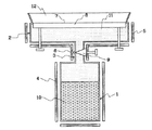
図1は、本発明による薄膜形成用分子線源の一実施形態を示す概略縦断側面図であり、図2はその平面図、図3はその薄膜形成用分子線源により基板sに薄膜の形成を行う状態を示す概略縦断側面図である。
【0018】
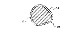
坩堝1には、成膜材料10が収納される。この場合、成膜材料10の蒸発効率を考慮し、特開2003−2778に開示されたように、成膜材料と共に、熱的、化学的に安定しており、且つ成膜材料15より熱伝導率の高い粒状の伝熱媒体を収納する。或いは、図4に示すように、粒状の伝熱媒体14をコアとして、その表面に成膜材料15を被覆するようにして設け、これを坩堝1の中に収納する。
【0019】
坩堝1の周囲には、加熱手段としてのヒータ4が配置され、これにより坩堝1の内部に成膜材料10が加熱され、それが昇華または蒸発して成膜材料10の分子を発生する。このとき伝熱媒体14は坩堝1の内部の伝熱を良好とし、成膜材料10の均一な昇華または蒸発を実現する。
【0020】
坩堝1の上端は、分子通過部3を介して圧力緩衝室2に通じている。この分子通過部3は坩堝1の上端から立ち上がった筒状のもので、その途中には第一のバルブ9としてニードルバルブが設けられている。分子通過部3はこの第一のバルブの開閉操作により開閉され、或いはその開口面積が調整される。
この坩堝1の分子通過部3の周囲にも加熱手段としてのヒータ6が配置され、分子通過部3の中の成膜材料の分子がその分子の状態に維持される。
【0021】
圧力緩衝室2は、その中央下部が前記分子通過部3の上端に通じた長尺な箱状のもので、ある一定の空間を有している。この圧力緩衝室2の上壁の中央にはその長手方向に沿って長尺スリット状の分子放出口7が開口している。この分子放出口7の周囲からは、上方に向けて漏斗状の分子放出ガイド12が設けられている。
【0022】
さらに、この分子放出口7には、長尺ブレード状の弁体の先端が挿入され、第二のバルブ8が構成されている。この第二のバルブ8の長尺ブレード状の弁体を上下することで、その先端で長尺スリット状の分子放出口7が開閉され、或いはその開口面積が調整される。従って、長尺ブレード状の弁体の長尺スリット状の分子放出口7の長さと同じである。
この圧力緩衝室2の周囲にも加熱手段としてのヒータ5が配置され、圧力緩衝室2の中の成膜材料の分子がその分子の状態に維持される。
【0023】
このような薄膜堆積用分子線源を使用し、基板sの成膜面上に薄膜を形成するには、まず第一のバルブ9と第二のバルブ8を閉じた状態で、ヒータ4により坩堝1の周囲からその中の成膜材料10を加熱し、それを昇華または蒸発して成膜材料10の分子を発生させる。このとき、第一のバルブ9と第二のバルブ8が閉じているため、比較的低い温度でも蒸気圧が高い有機EL材料のような成膜材料10であっても、その分子が坩堝1内から漏れない。そして、成膜材料10の昇華または蒸発を続けると、やがて坩堝1内では、成膜材料10の温度の応じた圧力で平衡に達する。もちろんこの状態ではヒータ6で分子通過部3を加熱しておく。
【0024】
このようにして坩堝1内が平衡圧に達した後、ヒータ5で圧力緩衝室2内を予め所定の温度に加熱した状態で、第一のバルブ9を開いて成膜材料の分子を圧力緩衝室2に導入する。このとき、第二のバルブ8を閉じておくことにより、やがて圧力緩衝室2内では、成膜材料10の温度の応じた圧力で平衡に達する。この状態では、圧力緩衝室2の全長にわたってその内部の成膜材料の分子の圧力をほぼ均一な圧力とすることが出来る。
【0025】
圧力緩衝室2内が所定の圧力で平衡状態に達した後、第二のバルブ8を開き、長尺スリット状の分子放出口7から成膜材料の分子を放出する。このとき、成膜材料の分子の圧力は、圧力緩衝室2の全長にわたってほぼ均一であるため、分子放出口7からは、その長手方向にわたって均一な量の成膜材料の分子が放出される。このとき、第一のバルブ9の開口面積に比べて、第二のバルブ8の開口面積を狭く調整することにより、圧力緩衝室2内での成膜材料の分子の圧力を安定して平衡状態に保つことが出来、成膜材料の分子の圧力を、圧力緩衝室2の全長にわたってほぼ均一に保つことが出来る。
【0026】
図3に示すように、基板sは、その成膜面を圧力緩衝室2の分子放出口7に対向して下向きに設置する。これにより、圧力緩衝室2の分子放出口7から放出された成膜材料の分子が基板sの成膜面に向けて放出され、その分子が基板sの成膜面に凝着して堆積し、薄膜が形成される。この場合において、圧力緩衝室2の分子放出口7と基板sの成膜面とを、分子放出口7の長手方向と直交する方向に相対移動させながら成膜する。この相対移動速度は、圧力緩衝室2の分子放出口7から単位時間当たりに放出される成膜材料の分子の量と基板sの成膜面上に成膜しようとする薄膜の膜厚との関係で決定される。相対移動であるから、圧力緩衝室2と基板sの一方または双方を移動させながらそれらの相対位置を変える。
【0027】
分子放出口7の周囲から起立した漏斗状の分子放出ガイド12は、分子放出口7から放出される分子の放出方向を制限し、その広がりを防止する。これにより、成膜効率の向上を図ることが出来る。
なお成膜の生産性を高めるため、圧力緩衝室2に複数の坩堝1を接続することも可能であり、生産性向上のため単位時間当たりの成膜材料の分子の放出量を多くする目的のためには特に有効である。
【0028】
図5に圧力緩衝室2の分子放出口7とそれを開閉し、その開口面積を調整する第二のバルブの構造の3つの例を示す。
図5(a)は、前述したように、分子放出口7をブレード状の弁体8aの先端を挿入し、その楔状の先端部で分子放出口7を開閉したり、或いはその開口面積を調整する例である。図5(b)は、板状の弁体9bを操作ピン12により上下動させ、これにより分子放出口7を開閉したり、或いはその開口面積を調整する例である。また、図5(c)は、部分円筒形の弁体9cを分子放出口7に接触させながら回転し、これにより分子放出口7を開閉したり、或いはその開口面積を調整する例である。
【0029】
【発明の効果】
以上説明した通り、本発明による薄膜堆積用分子線源とこれをを使用した薄膜堆積方法では、低温でも蒸気圧の高い成膜材料の分子でも、安定した分子の放出を行うことが出来る。長尺スリット状の分子放出口7分子放出口7の全長にわたってほぼ均一な質と量の分子を放射することが出来るので、分子放出口7と基板sとを分子放出口7の長手方向に相対移動させながら成膜することにより、基板sの成膜面上の広い面積にわたって均一な膜質と膜厚を有する薄膜を形成することが出来る。第一のバルブ9と第二のバルブ8の開閉により、低温でも蒸気圧が低い有機EL材料等の成膜材料であっても、意図しない分子の放出を最小限に抑えることが出来、成膜のコントロールが容易になる。
【図面の簡単な説明】
【図1】本発明による薄膜形成用分子線源の一実施形態を示す概略縦断側面図である。
【図2】薄膜形成用分子線源の同実施形態を示す平面図である。
【図3】同実施形態による膜形成用分子線源により基板に薄膜の形成を行う状態を示す概略縦断側面図である。
【図4】同実施形態による膜形成用分子線源により基板に薄膜の形成を行うに当たり、坩堝に収納するのに好ましい成膜材料の例を示す断面図である。
【図5】薄膜形成用分子線源の前記実施形態において、圧力緩衝室の分子放出口とそれを開閉し、その開口面積を調整する第二のバルブの構造の例を示す部分断面図である。
【符号の説明】
1 坩堝
2 圧力緩衝室
7 圧力緩衝室の分子放出口
8 第二のバルブ
9 第一のバルブ
10 成膜材料
s 基板[0001]
TECHNICAL FIELD OF THE INVENTION
According to the present invention, by heating a film-forming material, the film-forming material is sublimated or melted and evaporated to generate molecules of the film-forming material, and the molecules of the film-forming material are emitted toward a solid surface. The present invention relates to a thin film deposition molecular beam source cell used for growing a film by depositing molecules on a solid surface, and a thin film deposition method using the same.
[0002]
[Prior art]
A thin film deposition apparatus called a molecular beam epitaxy apparatus installs a substrate in a vacuum chamber capable of reducing the pressure to a high vacuum, heats the substrate to a required temperature, and moves a molecule such as a Knudsen cell toward a thin film growth surface of the substrate. A source cell is installed. The film-forming material stored in the crucible of the molecular beam source cell is heated by a heater to sublimate or melt and evaporate, and the generated molecules are incident on the thin film growth surface of the substrate, and the thin film is epitaxially grown on the surface. Then, a film of a film forming material is formed.
[0003]
The molecular beam source cell used in such a thin film deposition apparatus stores a film forming material in a crucible made of, for example, PBN (pyrrolytic boron nitride) having high thermal and chemical stability. Then, the film-forming material is heated by an electric heater provided outside the crucible, thereby sublimating or melting and evaporating the film-forming material to generate film-forming molecules.
[0004]
2. Description of the Related Art In recent years, research and development of organic electroluminescent elements (organic EL elements) have been promoted in fields such as displays and optical communications. This organic EL element is an element in which a light emitting layer is formed of an organic low molecular weight or organic high molecular weight material having EL light emitting ability, and its characteristics are attracting attention as a self-luminous type element. For example, the basic structure is such that a film of a hole transporting material such as triphenyldiamine (TPD) is formed on a hole injecting electrode, and a fluorescent substance such as an aluminum quinolinol complex (Alq 3 ) is laminated thereon as a light emitting layer. Further, a metal electrode having a small work function, such as Mg, Li, or Ca, is formed as an electron injection electrode.
[0005]
[Problems to be solved by the invention]
Recently, large screens have become a requirement of the times. Therefore, even in the display using the organic EL as described above, it is required to form an organic EL film on a large-sized substrate. In particular, in a display using an organic EL, it is required to form a uniform organic EL film on a substrate.
[0006]
However, as in a conventional vacuum deposition apparatus used for forming an organic EL film, a film forming material is sublimated or evaporated from one crucible to fire molecules on the surface of the substrate, and the film forming material is deposited. In the method of growing a film, it is difficult to form a uniform thin film on a large-area substrate.
[0007]
Further, when such an organic EL material is discharged from the molecule discharge port of the crucible toward the substrate and deposited on the substrate to form a film, if the distance between the molecule discharge port of the crucible and the film-forming surface of the substrate is short, The film thickness of the film-forming material becomes extremely thick at the portion facing the molecular emission port on the film-forming surface of the substrate, and the film thickness suddenly becomes thinner away from the portion facing the molecule emission port. That is, the uniformity of the film thickness is extremely deteriorated. Therefore, the film must be formed with a certain distance between the molecule discharge port of the crucible and the film forming surface of the substrate.
[0008]
However, the farther the molecular emission port of the crucible is separated from the film-forming surface of the substrate, the smaller the amount of the film-forming material actually deposited on the substrate with respect to the consumed film-forming material. There is a problem of getting worse. Since many organic EL materials are expensive, if the yield of film formation, that is, film formation efficiency, is low, this causes a high cost.
Furthermore, since the organic EL material has a high vapor pressure even at a low temperature, unintended vapor leakage from the crucible is likely to occur. For this reason, there is a problem that it is extremely difficult to control the film formation, and it is difficult to form a thin film having a target film quality and thickness.
[0009]
The present invention has been made in view of such problems in the conventional thin film deposition means, and can form a film having high uniformity of film thickness over a wide range on a film formation surface of a substrate while obtaining high film formation efficiency. It is another object of the present invention to provide a molecular beam source for depositing a thin film that does not cause unintended leakage of vapor from a crucible and that can easily control film formation, and a thin film deposition method using the same.
[0010]
[Means for Solving the Problems]
In the present invention, in order to achieve the above object, the molecules of the
[0011]
That is, the molecular beam source for depositing a thin film according to the present invention comprises a crucible 1 containing a
[0012]
The thin film deposition method according to the present invention for growing a thin film on a solid surface using the molecular beam source for thin film deposition according to the present invention has a smaller opening area of the
[0013]
In such a molecular beam source for thin film deposition according to the present invention and a thin film deposition method using the same, once the molecules of the
[0014]
In particular, by making the opening area of the
[0015]
In addition, the
[0016]
Further, a
[0017]
BEST MODE FOR CARRYING OUT THE INVENTION
Next, embodiments of the present invention will be described specifically and in detail with reference to the drawings.
FIG. 1 is a schematic longitudinal sectional side view showing an embodiment of a thin film forming molecular beam source according to the present invention, FIG. 2 is a plan view thereof, and FIG. 3 is a diagram showing the formation of a thin film on a substrate s by the thin film forming molecular beam source. FIG. 5 is a schematic vertical sectional side view showing a state in which the process is performed.
[0018]
A
[0019]
Around the crucible 1, a heater 4 as a heating means is arranged, whereby the
[0020]
The upper end of the crucible 1 communicates with the
A
[0021]
The
[0022]
Further, the tip of a long blade-shaped valve element is inserted into the
A
[0023]
In order to form a thin film on the film formation surface of the substrate s using such a thin film deposition molecular beam source, first, the crucible is heated by the heater 4 with the
[0024]
After the pressure inside the crucible 1 reaches the equilibrium pressure in this way, the
[0025]
After the inside of the
[0026]
As shown in FIG. 3, the substrate s is installed with its film-forming surface facing downward to the
[0027]
The funnel-shaped
It is also possible to connect a plurality of crucibles 1 to the
[0028]
FIG. 5 shows three examples of the structure of the
5A, as described above, the tip of the blade-shaped
[0029]
【The invention's effect】
As described above, the molecular beam source for thin film deposition and the thin film deposition method using the same according to the present invention can stably release molecules of a film forming material having a high vapor pressure even at a low temperature. Elongated slit-shaped
[Brief description of the drawings]
FIG. 1 is a schematic vertical sectional side view showing one embodiment of a molecular beam source for forming a thin film according to the present invention.
FIG. 2 is a plan view showing the same embodiment of the molecular beam source for forming a thin film.
FIG. 3 is a schematic vertical sectional side view showing a state in which a thin film is formed on a substrate by the film-forming molecular beam source according to the embodiment.
FIG. 4 is a cross-sectional view showing an example of a preferable film-forming material to be housed in a crucible when forming a thin film on a substrate by the film-forming molecular beam source according to the embodiment.
FIG. 5 is a partial cross-sectional view showing an example of the structure of a molecular discharge port of a pressure buffer chamber and a second valve for opening and closing the molecular discharge port and adjusting the opening area thereof in the embodiment of the molecular beam source for forming a thin film. .
[Explanation of symbols]
DESCRIPTION OF SYMBOLS 1
Claims (5)
Priority Applications (1)
| Application Number | Priority Date | Filing Date | Title |
|---|---|---|---|
| JP2003098936A JP4041005B2 (en) | 2003-04-02 | 2003-04-02 | Molecular beam source for thin film deposition and thin film deposition method using the same |
Applications Claiming Priority (1)
| Application Number | Priority Date | Filing Date | Title |
|---|---|---|---|
| JP2003098936A JP4041005B2 (en) | 2003-04-02 | 2003-04-02 | Molecular beam source for thin film deposition and thin film deposition method using the same |
Publications (2)
| Publication Number | Publication Date |
|---|---|
| JP2004307877A true JP2004307877A (en) | 2004-11-04 |
| JP4041005B2 JP4041005B2 (en) | 2008-01-30 |
Family
ID=33463534
Family Applications (1)
| Application Number | Title | Priority Date | Filing Date |
|---|---|---|---|
| JP2003098936A Expired - Lifetime JP4041005B2 (en) | 2003-04-02 | 2003-04-02 | Molecular beam source for thin film deposition and thin film deposition method using the same |
Country Status (1)
| Country | Link |
|---|---|
| JP (1) | JP4041005B2 (en) |
Cited By (21)
| Publication number | Priority date | Publication date | Assignee | Title |
|---|---|---|---|---|
| JP2006225725A (en) * | 2005-02-18 | 2006-08-31 | Hitachi Zosen Corp | Vapor deposition equipment |
| WO2007097329A1 (en) * | 2006-02-22 | 2007-08-30 | Tokyo Electron Limited | Film forming apparatus and method for manufacturing light emitting element |
| JP2008150649A (en) * | 2006-12-15 | 2008-07-03 | Tokki Corp | Vacuum deposition equipment |
| JP2008156726A (en) * | 2006-12-25 | 2008-07-10 | Matsushita Electric Works Ltd | Vacuum deposition system |
| JP2008156724A (en) * | 2006-12-25 | 2008-07-10 | Matsushita Electric Works Ltd | Vacuum deposition system |
| JP2008169456A (en) * | 2007-01-15 | 2008-07-24 | Matsushita Electric Works Ltd | Vacuum deposition system |
| JP2012504188A (en) * | 2008-09-29 | 2012-02-16 | アプライド マテリアルズ インコーポレイテッド | Vaporizer for organic materials |
| KR101149977B1 (en) * | 2005-02-03 | 2012-06-01 | 김명희 | Cell with linear crucible and selective nozzle for OLED deposition process |
| KR101232910B1 (en) | 2010-10-06 | 2013-02-13 | 엘아이지에이디피 주식회사 | apparatus for supplying organic matter, Apparatus and method for depositing organic matter using the same |
| JP2013519787A (en) * | 2010-02-16 | 2013-05-30 | アストロン フィアム セーフティー | Heating system for vapor deposition sources |
| JP2013108137A (en) * | 2011-11-21 | 2013-06-06 | Panasonic Corp | Inline vapor-deposition apparatus |
| JP5812496B2 (en) * | 2010-03-30 | 2015-11-11 | 国立大学法人神戸大学 | Thin film forming apparatus and thin film forming method |
| CN107041679A (en) * | 2017-06-13 | 2017-08-15 | 袁静 | An adjustable exhaust device for a rice steaming cabinet |
| CN107115016A (en) * | 2017-06-13 | 2017-09-01 | 袁静 | An easily adjustable rice steamer |
| JP2019099842A (en) * | 2017-11-29 | 2019-06-24 | 長州産業株式会社 | Vapor deposition apparatus, and vapor deposition method |
| JP2019214766A (en) * | 2018-06-13 | 2019-12-19 | 株式会社アルバック | Vapor deposition source for vacuum vapor deposition device |
| JP2019214767A (en) * | 2018-06-13 | 2019-12-19 | 株式会社アルバック | Vapor deposition source for vacuum vapor deposition device |
| KR20210008095A (en) * | 2018-06-15 | 2021-01-20 | 아르셀러미탈 | Vacuum deposition equipment and method for coating substrates |
| CN114622163A (en) * | 2020-12-10 | 2022-06-14 | 中国科学院大连化学物理研究所 | A Simple and Controllable Method for Molecular Evaporation |
| CN115726029A (en) * | 2022-12-07 | 2023-03-03 | 南京信光半导体科技有限公司 | Beam mechanical controllable molecular beam epitaxial metal element source furnace with valve block |
| CN117778961A (en) * | 2024-01-04 | 2024-03-29 | 中国科学院沈阳科学仪器股份有限公司 | A beam current control structure and control method of a high-temperature beam source furnace with built-in guide sleeves |
-
2003
- 2003-04-02 JP JP2003098936A patent/JP4041005B2/en not_active Expired - Lifetime
Cited By (30)
| Publication number | Priority date | Publication date | Assignee | Title |
|---|---|---|---|---|
| KR101149977B1 (en) * | 2005-02-03 | 2012-06-01 | 김명희 | Cell with linear crucible and selective nozzle for OLED deposition process |
| JP2006225725A (en) * | 2005-02-18 | 2006-08-31 | Hitachi Zosen Corp | Vapor deposition equipment |
| US8158012B2 (en) | 2006-02-22 | 2012-04-17 | Tokyo Electron Limited | Film forming apparatus and method for manufacturing light emitting element |
| WO2007097329A1 (en) * | 2006-02-22 | 2007-08-30 | Tokyo Electron Limited | Film forming apparatus and method for manufacturing light emitting element |
| JP2007227086A (en) * | 2006-02-22 | 2007-09-06 | Tokyo Electron Ltd | Film forming apparatus and light emitting element manufacturing method |
| JP2008150649A (en) * | 2006-12-15 | 2008-07-03 | Tokki Corp | Vacuum deposition equipment |
| JP2008156724A (en) * | 2006-12-25 | 2008-07-10 | Matsushita Electric Works Ltd | Vacuum deposition system |
| JP2008156726A (en) * | 2006-12-25 | 2008-07-10 | Matsushita Electric Works Ltd | Vacuum deposition system |
| JP2008169456A (en) * | 2007-01-15 | 2008-07-24 | Matsushita Electric Works Ltd | Vacuum deposition system |
| JP2012504188A (en) * | 2008-09-29 | 2012-02-16 | アプライド マテリアルズ インコーポレイテッド | Vaporizer for organic materials |
| JP2013519787A (en) * | 2010-02-16 | 2013-05-30 | アストロン フィアム セーフティー | Heating system for vapor deposition sources |
| JP5812496B2 (en) * | 2010-03-30 | 2015-11-11 | 国立大学法人神戸大学 | Thin film forming apparatus and thin film forming method |
| KR101232910B1 (en) | 2010-10-06 | 2013-02-13 | 엘아이지에이디피 주식회사 | apparatus for supplying organic matter, Apparatus and method for depositing organic matter using the same |
| JP2013108137A (en) * | 2011-11-21 | 2013-06-06 | Panasonic Corp | Inline vapor-deposition apparatus |
| CN107041679A (en) * | 2017-06-13 | 2017-08-15 | 袁静 | An adjustable exhaust device for a rice steaming cabinet |
| CN107115016A (en) * | 2017-06-13 | 2017-09-01 | 袁静 | An easily adjustable rice steamer |
| JP2019099842A (en) * | 2017-11-29 | 2019-06-24 | 長州産業株式会社 | Vapor deposition apparatus, and vapor deposition method |
| JP7036676B2 (en) | 2018-06-13 | 2022-03-15 | 株式会社アルバック | Thin-film deposition source for vacuum-film deposition equipment |
| JP2019214767A (en) * | 2018-06-13 | 2019-12-19 | 株式会社アルバック | Vapor deposition source for vacuum vapor deposition device |
| JP2019214766A (en) * | 2018-06-13 | 2019-12-19 | 株式会社アルバック | Vapor deposition source for vacuum vapor deposition device |
| JP7078462B2 (en) | 2018-06-13 | 2022-05-31 | 株式会社アルバック | Thin-film deposition source for vacuum-film deposition equipment |
| KR20210008095A (en) * | 2018-06-15 | 2021-01-20 | 아르셀러미탈 | Vacuum deposition equipment and method for coating substrates |
| JP2021526592A (en) * | 2018-06-15 | 2021-10-07 | アルセロールミタル | Vacuum deposition equipment and methods for substrate coating |
| JP7165755B2 (en) | 2018-06-15 | 2022-11-04 | アルセロールミタル | Vacuum deposition equipment and method for substrate coating |
| KR102538729B1 (en) | 2018-06-15 | 2023-05-31 | 아르셀러미탈 | Vacuum Deposition Equipment and Methods for Coating Substrates |
| US12129542B2 (en) | 2018-06-15 | 2024-10-29 | Arcelormittal | Vacuum deposition facility and method for coating a substrate with transverse repartition chamber |
| CN114622163A (en) * | 2020-12-10 | 2022-06-14 | 中国科学院大连化学物理研究所 | A Simple and Controllable Method for Molecular Evaporation |
| CN114622163B (en) * | 2020-12-10 | 2022-12-27 | 中国科学院大连化学物理研究所 | Simple and controllable molecular evaporation method |
| CN115726029A (en) * | 2022-12-07 | 2023-03-03 | 南京信光半导体科技有限公司 | Beam mechanical controllable molecular beam epitaxial metal element source furnace with valve block |
| CN117778961A (en) * | 2024-01-04 | 2024-03-29 | 中国科学院沈阳科学仪器股份有限公司 | A beam current control structure and control method of a high-temperature beam source furnace with built-in guide sleeves |
Also Published As
| Publication number | Publication date |
|---|---|
| JP4041005B2 (en) | 2008-01-30 |
Similar Documents
| Publication | Publication Date | Title |
|---|---|---|
| JP4041005B2 (en) | Molecular beam source for thin film deposition and thin film deposition method using the same | |
| KR100951493B1 (en) | A morecular beam epitaxy effusion cell for use in vacuum thin film deposition and a method therefor | |
| JP4704605B2 (en) | Continuous vapor deposition apparatus, vapor deposition apparatus and vapor deposition method | |
| TWI420721B (en) | Vapor deposition source and method | |
| US7238389B2 (en) | Vaporizing fluidized organic materials | |
| KR100826743B1 (en) | Organic thin film manufacturing apparatus | |
| US20050244580A1 (en) | Deposition apparatus for temperature sensitive materials | |
| US20110033973A1 (en) | Deposition apparatus for temperature sensitive materials | |
| US7364772B2 (en) | Method for coating an organic layer onto a substrate in a vacuum chamber | |
| JP3684343B2 (en) | Molecular beam source cell for thin film deposition | |
| JP3754380B2 (en) | Molecular beam source cell for thin film deposition and thin film deposition method | |
| JP3756458B2 (en) | Molecular beam source cell for thin film deposition | |
| JP3802846B2 (en) | Molecular beam source cell for thin film deposition | |
| KR20060013735A (en) | Continuous Crucible Exchange Device for Continuous Deposition of Organic EL Devices | |
| JP3616586B2 (en) | Molecular beam source cell for thin film deposition | |
| JP2003155555A (en) | Multiple molecular beam source cell for thin film deposition | |
| KR20070066232A (en) | Deposition equipment | |
| JP2007224393A (en) | Vapor deposition source cell, thin film deposition method, aperture diaphragm member, and vapor deposition source heater | |
| KR101037121B1 (en) | Deposition apparatus and deposition method | |
| KR20030067146A (en) | Heating crucible of deposit apparatus | |
| JP2004162108A (en) | Molecular beam source cell for thin film deposition | |
| KR100700497B1 (en) | Evaporating apparatus | |
| JP4491449B2 (en) | Molecular beam source cell for thin film deposition | |
| KR20230115678A (en) | Lateral type vacuum effusion cell and method for fabricating organic light emitting display device using the same | |
| KR20050090843A (en) | Apparatus for linearly heating deposition source material |
Legal Events
| Date | Code | Title | Description |
|---|---|---|---|
| A621 | Written request for application examination |
Free format text: JAPANESE INTERMEDIATE CODE: A621 Effective date: 20041213 |
|
| A977 | Report on retrieval |
Free format text: JAPANESE INTERMEDIATE CODE: A971007 Effective date: 20070820 |
|
| A131 | Notification of reasons for refusal |
Free format text: JAPANESE INTERMEDIATE CODE: A131 Effective date: 20070822 |
|
| A521 | Request for written amendment filed |
Free format text: JAPANESE INTERMEDIATE CODE: A523 Effective date: 20070828 |
|
| A711 | Notification of change in applicant |
Free format text: JAPANESE INTERMEDIATE CODE: A711 Effective date: 20070914 |
|
| TRDD | Decision of grant or rejection written | ||
| A521 | Request for written amendment filed |
Free format text: JAPANESE INTERMEDIATE CODE: A821 Effective date: 20070914 |
|
| A01 | Written decision to grant a patent or to grant a registration (utility model) |
Free format text: JAPANESE INTERMEDIATE CODE: A01 Effective date: 20071102 |
|
| A61 | First payment of annual fees (during grant procedure) |
Free format text: JAPANESE INTERMEDIATE CODE: A61 Effective date: 20071108 |
|
| FPAY | Renewal fee payment (event date is renewal date of database) |
Free format text: PAYMENT UNTIL: 20101116 Year of fee payment: 3 |
|
| R150 | Certificate of patent or registration of utility model |
Ref document number: 4041005 Country of ref document: JP Free format text: JAPANESE INTERMEDIATE CODE: R150 |
|
| FPAY | Renewal fee payment (event date is renewal date of database) |
Free format text: PAYMENT UNTIL: 20101116 Year of fee payment: 3 |
|
| FPAY | Renewal fee payment (event date is renewal date of database) |
Free format text: PAYMENT UNTIL: 20111116 Year of fee payment: 4 |
|
| R250 | Receipt of annual fees |
Free format text: JAPANESE INTERMEDIATE CODE: R250 |
|
| FPAY | Renewal fee payment (event date is renewal date of database) |
Free format text: PAYMENT UNTIL: 20111116 Year of fee payment: 4 |
|
| FPAY | Renewal fee payment (event date is renewal date of database) |
Free format text: PAYMENT UNTIL: 20121116 Year of fee payment: 5 |
|
| R250 | Receipt of annual fees |
Free format text: JAPANESE INTERMEDIATE CODE: R250 |
|
| FPAY | Renewal fee payment (event date is renewal date of database) |
Free format text: PAYMENT UNTIL: 20121116 Year of fee payment: 5 |
|
| FPAY | Renewal fee payment (event date is renewal date of database) |
Free format text: PAYMENT UNTIL: 20131116 Year of fee payment: 6 |
|
| R250 | Receipt of annual fees |
Free format text: JAPANESE INTERMEDIATE CODE: R250 |
|
| R250 | Receipt of annual fees |
Free format text: JAPANESE INTERMEDIATE CODE: R250 |
|
| R250 | Receipt of annual fees |
Free format text: JAPANESE INTERMEDIATE CODE: R250 |
|
| R250 | Receipt of annual fees |
Free format text: JAPANESE INTERMEDIATE CODE: R250 |
|
| R250 | Receipt of annual fees |
Free format text: JAPANESE INTERMEDIATE CODE: R250 |
|
| R250 | Receipt of annual fees |
Free format text: JAPANESE INTERMEDIATE CODE: R250 |
|
| R250 | Receipt of annual fees |
Free format text: JAPANESE INTERMEDIATE CODE: R250 |
|
| R250 | Receipt of annual fees |
Free format text: JAPANESE INTERMEDIATE CODE: R250 |
|
| R250 | Receipt of annual fees |
Free format text: JAPANESE INTERMEDIATE CODE: R250 |
|
| R250 | Receipt of annual fees |
Free format text: JAPANESE INTERMEDIATE CODE: R250 |
|
| R250 | Receipt of annual fees |
Free format text: JAPANESE INTERMEDIATE CODE: R250 |
|
| EXPY | Cancellation because of completion of term |