【0001】
【発明の属する技術分野】
本発明は表面実装部品とプリント配線基板との間に載置され、表面実装部品とプリント配線基板とをはんだ接続し乃至取り外すために用いられるヒートコネクタに関する。
【0002】
【従来の技術】
プリント配線基板上に実装する表面実装部品としてBGA(Ball Grid Array)パッケージやLGA(Land Grid Array)パッケージあるいはSOM(Small Outline Non Lead)といったものがある。
【0003】
このうち、たとえばBGAパッケージをプリント配線基板に接続し、乃至取り外す際の従来方法を説明する。
【0004】
図5は、従来のBGAパッケージの回路試験に用いられるソケットを用いたコネクタ方式による接続方法を示す断面図である。
【0005】
中継ソケット17にははんだバンプ2cが設けられている。プリント配線基板8上のランド(不図示)ははんだバンプ2cに対応して配置されている。BGAソケット18をプリント配線基板8上に配置してリフロー加熱をすることではんだバンプ2cがプリント配線基板8とはんだ接続する。
【0006】
また、BGAパッケージ1の底面に配置されたはんだバンプ2bのそれぞれをBGAソケット18に埋設された接触ピン15の端面に対し対応させて接触させ、加圧ネジ14を締める事で加圧機構13により加圧固定する。
【0007】
その結果、BGAパッケージ1とプリント配線基板8は電気的に接続される。
【0008】
この状態でBGAパッケージ1に対し必要な回路試験を行なう事ができる。
【0009】
BGAパッケージ1を取り外すには、加圧ネジ14を緩めて加圧機構13による加圧力を取り除き、BGAパッケージ1をBGAソケット18から分離すれば良い。
【0010】
また、他の方法として、熱風によりBGAパッケージ1及びプリント配線基板8を加熱しBGAパッケージ1に配置された、はんだバンプ2bを溶融させることでBGAパッケージ1とプリント配線基板8とを直接はんだ接続し、乃至取り外しを行なう。
【0011】
本発明者は既に特願2001−320614号において、貫通導電体として導電性ペーストを充填する方式のものを出願している。これはペースト混合物の金属がはんだに拡散することによりペースト内金属の残留量が減少する傾向があり、貫通導電体の接合機能を阻害する要素を持っている。
【0012】
そこで、上記導電性ペーストを金属ピンに変えることではんだとの合金形成による貫通導電材料の機能維持、耐久性を格段に向上させたものである。
【0013】
【発明が解決しようとする課題】
前記2つの従来の方式では、選択的加熱専用の比較的大型な設備を必要とするため、BGAパッケージを取り外し乃至接続しながら回路試験を行なえる場所が限定されるという問題点があった。
【0014】
また、ソケットによるコネクタ方式はソケットが大型となり、周囲の部品との干渉、製品筐体に組み込む場合の周囲の機構部との干渉があり、製品に組み込むプリント配線基板上に設けるのに困難があった。
【0015】
また、BGAパッケージ1とプリント配線基板8とを直接はんだ接続し、乃至取り外しを行なう方法でははんだ溶融に至るまでに表面実装部品であるBGAパッケージ本体が過剰に加熱されることでBGAパッケージ内のIC機能を損傷するという問題点があった。
【0016】
本発明は前記従来技術の問題点に鑑み、表面実装部品の機能を損傷する事なく、また、大型設備を使用せずに表面実装部品をプリント配線基板にはんだ接続乃至取り外しを可能とするヒートコネクタを提供することを目的とする。
【0017】
また、プリント配線基板上にスペースを取らずに表面実装部品をはんだ接続可能なヒートコネクタを提供することを目的とする。
【0018】
さらにはこのようなヒートコネクタを用いて表面実装部品が実装されたプリント配線基板を提供する事を目的とする。
【0019】
【課題を解決するための手段】
前記目的を達成するため、本発明によるヒートコネクタは、以下(1)、(2)の構成を備える。
【0020】
(1)アレイ状の外部端子を有する表面実装部品(以下表面実装部品という)とプリント配線基板との間に載置されて前記表面実装部品と前記プリント配線基板とをはんだ接続し乃至取り外す際に用いるヒートコネクタであって、絶縁性基体と、前記アレイ状の外部端子に対応して前記絶縁性基体中に貫通して埋め込まれた複数の導電体と、これとは絶縁された状態で前記絶縁性基体を通電加熱するための抵抗体からなり、前記複数の導電体が金属ピンであることを特徴とするヒートコネクタ。
【0021】
(2)前記金属ピンが絶縁性基体の表面より突き出ていることを特徴とする上記(1)に記載のヒートコネクタ。
【0022】
【発明の実施の形態】
以下、本発明の実施の形態を図面に基づき説明する。
【0023】
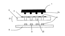
図1は本発明の、第1の実施の形態によるヒートコネクタ21を表面実装部品の一種であるBGAパッケージ1とプリント配線基板8間に配置した、はんだ接続前の状態を示す断面図である。
【0024】
プリント配線基板8上にはランド9が形成されておりランド9上にはクリームはんだ4が塗布されている。ランド9はプリント配線基板8上でBGAパッケージ1の底面に載置されている、はんだバンプ2aに対応する位置に配置されている。
【0025】
ヒートコネクタ21は絶縁性基体であるヒートコネクタ基材6中に貫通する金属ピン22及びヒートコネクタ基材6の表面に形成された抵抗体3よりなる。ヒートコネクタ基材6は絶縁性材料として、特にアルミナ等のセラミック材料が適している。これは、ヒートコネクタ21をプリント配線基板8上に載置する際のハンドリング性確保、及びはんだ溶融の加熱によりヒートコネクタ基材6の変形が生じないようにするためである。
【0026】
ヒートコネクタ基材6にあらかじめドリル加工やレーザ加工等により貫通孔を形成しておき、この貫通孔内に金属ピン22を挿入しヒートコネクタ基材6表面に露出した端面上にクリームはんだ4を塗布する。
【0027】
抵抗体3は、例えばAg、Pd、Ru、Cuを含む合金あるいはこれら金属の酸化物よりなり、印刷法でヒートコネクタ基材6表面上にパターン印刷した後加熱焼成して形成する。
【0028】
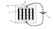
図2に示すように本実施の形態では、抵抗体3は複数の平行な帯として形成し、各抵抗体3は金属ピン22と電気的に絶縁されている。抵抗体3の各端部はそれぞれ抵抗体接続回路10へ接続されている。
【0029】
抵抗体電流印加端子11には外部の電源12が直列に接続され、不図示の制御装置で通電制御される。
【0030】
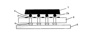
図3はBGAパッケージ1、ヒートコネクタ基材6、プリント配線基板8を近接配置した状態を示す。この状態で抵抗体接続回路10に通電すると、抵抗体3が発熱し、この熱によりクリームはんだ4及びはんだバンプ2aを溶融し、BGAパッケージ1とプリント配線基板8がはんだにより導電接合される。
【0031】
プリント配線基板8に、はんだ接合したBGAパッケージ1をプリント配線基板8から取り外すには、接合時と同様に抵抗体3に電流を印加することで抵抗体からの発熱によりはんだを溶融し、BGAパッケージ1とプリント配線基板8を引き離せばよい。
【0032】
プリント配線基板8から取り外されたBGAパッケージ1を再度プリント配線基板8に接続する場合、BGAパッケージ1には既にはんだバンプ2aが失われた状態となっているが、金属ピン22の上にクリームはんだ4を再度、塗布することによってヒートコネクタ21とBGAパッケージ1のはんだバンプが載置されていた電極とのはんだ接合が可能である。
【0033】
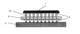
次に、図4に本発明の、第2の実施の形態を示す。
【0034】
この実施の形態によれば、金属ピン22の形状をヒートコネクタ基材6より突き出した金属ピン23にしたことにより、はんだバンプ2aが失われた状態のBGAパッケージ1を再度、はんだ接合する場合、クリームはんだ4をBGA底面の電極に塗布し、突き出し金属ピン23と対応させて図4のように近接配置し、また同様にプリント配線基板8側も突き出した構造にしてプリント配線基板8に塗布したクリームはんだ4にて接合する。
【0035】
この構造の利点は、ヒートコネクタ基材6とBGAパッケージ1及びプリント配線基板8相互間の熱膨張係数の差、その他構造的歪をこの突き出し部分で吸収することが可能である、と共にクリームはんだが金属ピン間を短絡することを防止することができる。
【0036】
【発明の効果】
以上説明したように、本発明のヒートコネクタ21によればヒートコネクタ21に設けた抵抗体からの発熱によって表面実装部品のはんだバンプを選択的に加熱することができるため、表面実装部品の熱損傷を大幅に押さえることができる。
【0037】
また、抵抗体からの熱はヒートコネクタ21中に埋め込まれた金属ピン22を伝導するため、はんだ接合部分を効率よく加熱する事ができる。
【0038】
さらには、従来のように大型設備を必要としないため、どのような場所においても表面実装部品を用いたプリント配線基板の回路試験が可能となる。
【図面の簡単な説明】
【図1】本発明の、第1の実施の形態によるヒートコネクタをBGAパッケージとプリント配線基板間に配置した、はんだ接合前の状態を示す断面図
【図2】本発明の、第1の実施の形態によるヒートコネクタをプリント配線基板上に配置した状態を示す上面図
【図3】本発明の、第1の実施の形態によるヒートコネクタをBGAパッケージとプリント配線基板間に近接配置した後の状態を示す断面図
【図4】本発明の、第2の実施の形態による突き出し金属ピン構造によるヒートコネクタを、BGAパッケージとプリント配線基板間に近接配置した後の状態を示す断面図
【図5】従来のBGAパッケージの回路試験に用いられるソケットを基板に配置した状態を示す断面図
【符号の説明】
1 BGAパッケージ
2a、2b、2c はんだバンプ
3 抵抗体
4 クリームはんだ
6 ヒートコネクタ基材
8 プリント配線基板
9 ランド
10 抵抗体接続回路
11 抵抗体電流印加端子
12 電源
13 加圧機構
14 加圧ネジ
15 接触ピン
16 接触ピン保持板
17 中継ソケット
18 BGAソケット
21 ヒートコネクタ
22 金属ピン
23 突き出し金属ピン[0001]
TECHNICAL FIELD OF THE INVENTION
The present invention relates to a heat connector which is mounted between a surface mount component and a printed wiring board and is used for connecting or disconnecting the surface mount component and the printed wiring board by soldering.
[0002]
[Prior art]
Surface mount components mounted on a printed wiring board include a BGA (Ball Grid Array) package, an LGA (Land Grid Array) package, and an SOM (Small Outline Non Lead).
[0003]
Among them, for example, a conventional method for connecting or removing a BGA package to or from a printed wiring board will be described.
[0004]
FIG. 5 is a cross-sectional view showing a connection method by a connector method using a socket used for a circuit test of a conventional BGA package.
[0005]
The relay socket 17 is provided with a solder bump 2c. The lands (not shown) on the printed wiring board 8 are arranged corresponding to the solder bumps 2c. The BGA socket 18 is arranged on the printed wiring board 8 and subjected to reflow heating, so that the solder bumps 2c are connected to the printed wiring board 8 by soldering.
[0006]
Further, each of the solder bumps 2 b arranged on the bottom surface of the BGA package 1 is brought into contact with the end surface of the contact pin 15 embedded in the BGA socket 18, and the pressing mechanism 13 is tightened by pressing the pressing screw 14. Press and fix.
[0007]
As a result, the BGA package 1 and the printed wiring board 8 are electrically connected.
[0008]
In this state, a necessary circuit test can be performed on the BGA package 1.
[0009]
To remove the BGA package 1, the pressing screw 14 is loosened to remove the pressing force by the pressing mechanism 13, and the BGA package 1 may be separated from the BGA socket 18.
[0010]
Further, as another method, the BGA package 1 and the printed wiring board 8 are heated by hot air to melt the solder bumps 2b disposed on the BGA package 1 so that the BGA package 1 and the printed wiring board 8 are directly solder-connected. , Or removal.
[0011]
The present inventor has already filed an application in Japanese Patent Application No. 2001-320614 for filling a conductive paste as a penetrating conductor. This tends to reduce the residual amount of the metal in the paste due to the diffusion of the metal of the paste mixture into the solder, and has an element that hinders the bonding function of the through conductor.
[0012]
Therefore, by changing the conductive paste into metal pins, the function maintenance and durability of the penetrating conductive material by forming an alloy with solder are remarkably improved.
[0013]
[Problems to be solved by the invention]
The above two conventional methods require a relatively large facility dedicated to selective heating, and thus have a problem that the place where a circuit test can be performed while removing or connecting the BGA package is limited.
[0014]
In addition, the socket-type connector system has a large socket, which causes interference with surrounding components and interference with surrounding mechanical parts when incorporated into the product housing, making it difficult to provide the product on a printed wiring board that is incorporated into the product. Was.
[0015]
In the method of directly connecting and disconnecting the BGA package 1 and the printed wiring board 8 and removing the same, the BGA package body which is a surface mount component is excessively heated until the solder is melted, so that the IC in the BGA package is heated. There was a problem that the function was damaged.
[0016]
SUMMARY OF THE INVENTION In view of the problems of the prior art, the present invention provides a heat connector that allows a surface mount component to be connected to or detached from a printed circuit board without damaging the function of the surface mount component and without using large-scale equipment. The purpose is to provide.
[0017]
It is another object of the present invention to provide a heat connector capable of soldering surface mount components without taking up space on a printed wiring board.
[0018]
It is another object of the present invention to provide a printed wiring board on which surface mount components are mounted using such a heat connector.
[0019]
[Means for Solving the Problems]
In order to achieve the above object, a heat connector according to the present invention has the following configurations (1) and (2).
[0020]
(1) When mounting between a surface mount component having an array of external terminals (hereinafter referred to as a surface mount component) and a printed wiring board to solder or remove the surface mount component and the printed wiring board, A heat connector to be used, comprising: an insulating base; a plurality of conductors penetratingly embedded in the insulating base corresponding to the array-like external terminals; A heat connector comprising a resistor for electrically heating a conductive substrate, wherein the plurality of conductors are metal pins.
[0021]
(2) The heat connector according to (1), wherein the metal pins protrude from a surface of the insulating substrate.
[0022]
BEST MODE FOR CARRYING OUT THE INVENTION
Hereinafter, embodiments of the present invention will be described with reference to the drawings.
[0023]
FIG. 1 is a cross-sectional view showing a state before solder connection, in which a heat connector 21 according to a first embodiment of the present invention is arranged between a BGA package 1 which is a kind of surface mount component and a printed wiring board 8.
[0024]
A land 9 is formed on the printed wiring board 8, and the cream solder 4 is applied on the land 9. The lands 9 are disposed on the printed wiring board 8 at positions corresponding to the solder bumps 2a mounted on the bottom surface of the BGA package 1.
[0025]
The heat connector 21 includes metal pins 22 penetrating into the heat connector base 6 which is an insulating base, and the resistor 3 formed on the surface of the heat connector base 6. As the insulating material, the ceramic material such as alumina is particularly suitable for the heat connector base material 6. This is to ensure the handleability when mounting the heat connector 21 on the printed wiring board 8 and to prevent the deformation of the heat connector base 6 due to the heating of the solder melt.
[0026]
A through hole is previously formed in the heat connector base material 6 by drilling, laser processing, or the like, and a metal pin 22 is inserted into the through hole, and the cream solder 4 is applied to the end surface exposed on the surface of the heat connector base material 6. I do.
[0027]
The resistor 3 is made of, for example, an alloy containing Ag, Pd, Ru, or Cu or an oxide of these metals. The resistor 3 is formed by printing a pattern on the surface of the heat connector base 6 by a printing method and then heating and baking.
[0028]
As shown in FIG. 2, in the present embodiment, the resistors 3 are formed as a plurality of parallel bands, and each resistor 3 is electrically insulated from the metal pin 22. Each end of the resistor 3 is connected to the resistor connection circuit 10.
[0029]
An external power supply 12 is connected to the resistor current application terminal 11 in series, and energization is controlled by a control device (not shown).
[0030]
FIG. 3 shows a state in which the BGA package 1, the heat connector base material 6, and the printed wiring board 8 are arranged close to each other. When the resistor connection circuit 10 is energized in this state, the resistor 3 generates heat, and the heat melts the cream solder 4 and the solder bump 2a, so that the BGA package 1 and the printed wiring board 8 are conductively joined by solder.
[0031]
In order to remove the BGA package 1 soldered to the printed wiring board 8 from the printed wiring board 8, a current is applied to the resistor 3 as in the case of joining, the solder is melted by heat generated from the resistor, and the BGA package is removed. 1 and the printed wiring board 8 may be separated from each other.
[0032]
When the BGA package 1 removed from the printed wiring board 8 is connected to the printed wiring board 8 again, the BGA package 1 has already lost the solder bumps 2a. 4 is applied again, so that the heat connector 21 and the electrode of the BGA package 1 on which the solder bumps are mounted can be soldered.
[0033]
Next, FIG. 4 shows a second embodiment of the present invention.
[0034]
According to this embodiment, when the shape of the metal pins 22 is changed to the metal pins 23 protruding from the heat connector base material 6, when the BGA package 1 in a state where the solder bumps 2a are lost is soldered again, The cream solder 4 was applied to the electrode on the bottom surface of the BGA, and was arranged close to the protruding metal pin 23 as shown in FIG. 4, and was similarly applied to the printed wiring board 8 so that the printed wiring board 8 side also protruded. Join with cream solder 4.
[0035]
The advantage of this structure is that the difference in thermal expansion coefficient between the heat connector base 6 and the BGA package 1 and the printed wiring board 8 and other structural distortions can be absorbed by the protruding portion, and the cream solder can be used. A short circuit between the metal pins can be prevented.
[0036]
【The invention's effect】
As described above, according to the heat connector 21 of the present invention, the solder bumps of the surface mount component can be selectively heated by the heat generated from the resistor provided on the heat connector 21, and thus the heat damage of the surface mount component can be prevented. Can be greatly reduced.
[0037]
Further, since the heat from the resistor is conducted through the metal pin 22 embedded in the heat connector 21, the solder joint can be efficiently heated.
[0038]
Furthermore, since large equipment is not required unlike the conventional case, a circuit test of a printed wiring board using a surface mount component can be performed at any place.
[Brief description of the drawings]
FIG. 1 is a cross-sectional view showing a state before solder bonding in which a heat connector according to a first embodiment of the present invention is arranged between a BGA package and a printed wiring board. FIG. 2 is a first embodiment of the present invention. FIG. 3 is a top view showing a state in which the heat connector according to the embodiment is arranged on a printed wiring board; FIG. 3 is a view showing a state after the heat connector according to the first embodiment of the present invention is arranged close to the BGA package and the printed wiring board; FIG. 4 is a cross-sectional view showing a state after a heat connector having a protruding metal pin structure according to a second embodiment of the present invention is disposed close to a BGA package and a printed wiring board; Sectional view showing a state where a socket used for a circuit test of a conventional BGA package is arranged on a substrate.
DESCRIPTION OF SYMBOLS 1 BGA package 2a, 2b, 2c Solder bump 3 Resistor 4 Cream solder 6 Heat connector base material 8 Printed wiring board 9 Land 10 Resistor connection circuit 11 Resistor current application terminal 12 Power supply 13 Pressure mechanism 14 Pressure screw 15 Contact Pin 16 Contact pin holding plate 17 Relay socket 18 BGA socket 21 Heat connector 22 Metal pin 23 Projecting metal pin