JP2004341486A - 液晶表示装置および電子機器 - Google Patents
液晶表示装置および電子機器 Download PDFInfo
- Publication number
- JP2004341486A JP2004341486A JP2004031060A JP2004031060A JP2004341486A JP 2004341486 A JP2004341486 A JP 2004341486A JP 2004031060 A JP2004031060 A JP 2004031060A JP 2004031060 A JP2004031060 A JP 2004031060A JP 2004341486 A JP2004341486 A JP 2004341486A
- Authority
- JP
- Japan
- Prior art keywords
- liquid crystal
- region
- dot
- area
- display
- Prior art date
- Legal status (The legal status is an assumption and is not a legal conclusion. Google has not performed a legal analysis and makes no representation as to the accuracy of the status listed.)
- Granted
Links
- 239000004973 liquid crystal related substance Substances 0.000 title claims abstract description 239
- 239000000758 substrate Substances 0.000 claims abstract description 66
- 230000005684 electric field Effects 0.000 claims abstract description 20
- 230000005540 biological transmission Effects 0.000 claims description 11
- 238000003491 array Methods 0.000 abstract description 2
- 230000001747 exhibiting effect Effects 0.000 abstract 1
- 239000010408 film Substances 0.000 description 76
- 230000004048 modification Effects 0.000 description 62
- 238000012986 modification Methods 0.000 description 62
- 239000011159 matrix material Substances 0.000 description 9
- 230000000694 effects Effects 0.000 description 7
- 230000001105 regulatory effect Effects 0.000 description 7
- 238000010586 diagram Methods 0.000 description 5
- 208000037265 diseases, disorders, signs and symptoms Diseases 0.000 description 5
- 239000011521 glass Substances 0.000 description 4
- 239000004033 plastic Substances 0.000 description 4
- 239000010453 quartz Substances 0.000 description 4
- VYPSYNLAJGMNEJ-UHFFFAOYSA-N silicon dioxide Inorganic materials O=[Si]=O VYPSYNLAJGMNEJ-UHFFFAOYSA-N 0.000 description 4
- 229910052782 aluminium Inorganic materials 0.000 description 3
- 229910052751 metal Inorganic materials 0.000 description 3
- 239000002184 metal Substances 0.000 description 3
- 238000000034 method Methods 0.000 description 3
- 239000004925 Acrylic resin Substances 0.000 description 2
- 229920000178 Acrylic resin Polymers 0.000 description 2
- XAGFODPZIPBFFR-UHFFFAOYSA-N aluminium Chemical compound [Al] XAGFODPZIPBFFR-UHFFFAOYSA-N 0.000 description 2
- 230000015572 biosynthetic process Effects 0.000 description 2
- 239000003086 colorant Substances 0.000 description 2
- 210000002858 crystal cell Anatomy 0.000 description 2
- 229910052709 silver Inorganic materials 0.000 description 2
- 238000002834 transmittance Methods 0.000 description 2
- 206010047571 Visual impairment Diseases 0.000 description 1
- 210000004027 cell Anatomy 0.000 description 1
- 230000007547 defect Effects 0.000 description 1
- AMGQUBHHOARCQH-UHFFFAOYSA-N indium;oxotin Chemical compound [In].[Sn]=O AMGQUBHHOARCQH-UHFFFAOYSA-N 0.000 description 1
- 238000010030 laminating Methods 0.000 description 1
- 239000000463 material Substances 0.000 description 1
- 230000003287 optical effect Effects 0.000 description 1
- 230000003071 parasitic effect Effects 0.000 description 1
- 230000002093 peripheral effect Effects 0.000 description 1
- 230000010287 polarization Effects 0.000 description 1
- 238000002310 reflectometry Methods 0.000 description 1
- 239000004332 silver Substances 0.000 description 1
- 239000010409 thin film Substances 0.000 description 1
Images










Classifications
-
- F—MECHANICAL ENGINEERING; LIGHTING; HEATING; WEAPONS; BLASTING
- F16—ENGINEERING ELEMENTS AND UNITS; GENERAL MEASURES FOR PRODUCING AND MAINTAINING EFFECTIVE FUNCTIONING OF MACHINES OR INSTALLATIONS; THERMAL INSULATION IN GENERAL
- F16L—PIPES; JOINTS OR FITTINGS FOR PIPES; SUPPORTS FOR PIPES, CABLES OR PROTECTIVE TUBING; MEANS FOR THERMAL INSULATION IN GENERAL
- F16L41/00—Branching pipes; Joining pipes to walls
- F16L41/08—Joining pipes to walls or pipes, the joined pipe axis being perpendicular to the plane of a wall or to the axis of another pipe
- F16L41/14—Joining pipes to walls or pipes, the joined pipe axis being perpendicular to the plane of a wall or to the axis of another pipe by screwing an intermediate part against the inside or outside of the wall
-
- G—PHYSICS
- G02—OPTICS
- G02F—OPTICAL DEVICES OR ARRANGEMENTS FOR THE CONTROL OF LIGHT BY MODIFICATION OF THE OPTICAL PROPERTIES OF THE MEDIA OF THE ELEMENTS INVOLVED THEREIN; NON-LINEAR OPTICS; FREQUENCY-CHANGING OF LIGHT; OPTICAL LOGIC ELEMENTS; OPTICAL ANALOGUE/DIGITAL CONVERTERS
- G02F1/00—Devices or arrangements for the control of the intensity, colour, phase, polarisation or direction of light arriving from an independent light source, e.g. switching, gating or modulating; Non-linear optics
- G02F1/01—Devices or arrangements for the control of the intensity, colour, phase, polarisation or direction of light arriving from an independent light source, e.g. switching, gating or modulating; Non-linear optics for the control of the intensity, phase, polarisation or colour
- G02F1/13—Devices or arrangements for the control of the intensity, colour, phase, polarisation or direction of light arriving from an independent light source, e.g. switching, gating or modulating; Non-linear optics for the control of the intensity, phase, polarisation or colour based on liquid crystals, e.g. single liquid crystal display cells
- G02F1/133—Constructional arrangements; Operation of liquid crystal cells; Circuit arrangements
- G02F1/1333—Constructional arrangements; Manufacturing methods
- G02F1/1337—Surface-induced orientation of the liquid crystal molecules, e.g. by alignment layers
- G02F1/133753—Surface-induced orientation of the liquid crystal molecules, e.g. by alignment layers with different alignment orientations or pretilt angles on a same surface, e.g. for grey scale or improved viewing angle
-
- F—MECHANICAL ENGINEERING; LIGHTING; HEATING; WEAPONS; BLASTING
- F16—ENGINEERING ELEMENTS AND UNITS; GENERAL MEASURES FOR PRODUCING AND MAINTAINING EFFECTIVE FUNCTIONING OF MACHINES OR INSTALLATIONS; THERMAL INSULATION IN GENERAL
- F16L—PIPES; JOINTS OR FITTINGS FOR PIPES; SUPPORTS FOR PIPES, CABLES OR PROTECTIVE TUBING; MEANS FOR THERMAL INSULATION IN GENERAL
- F16L41/00—Branching pipes; Joining pipes to walls
- F16L41/08—Joining pipes to walls or pipes, the joined pipe axis being perpendicular to the plane of a wall or to the axis of another pipe
- F16L41/16—Joining pipes to walls or pipes, the joined pipe axis being perpendicular to the plane of a wall or to the axis of another pipe the branch pipe comprising fluid cut-off means
-
- G—PHYSICS
- G02—OPTICS
- G02F—OPTICAL DEVICES OR ARRANGEMENTS FOR THE CONTROL OF LIGHT BY MODIFICATION OF THE OPTICAL PROPERTIES OF THE MEDIA OF THE ELEMENTS INVOLVED THEREIN; NON-LINEAR OPTICS; FREQUENCY-CHANGING OF LIGHT; OPTICAL LOGIC ELEMENTS; OPTICAL ANALOGUE/DIGITAL CONVERTERS
- G02F1/00—Devices or arrangements for the control of the intensity, colour, phase, polarisation or direction of light arriving from an independent light source, e.g. switching, gating or modulating; Non-linear optics
- G02F1/01—Devices or arrangements for the control of the intensity, colour, phase, polarisation or direction of light arriving from an independent light source, e.g. switching, gating or modulating; Non-linear optics for the control of the intensity, phase, polarisation or colour
- G02F1/13—Devices or arrangements for the control of the intensity, colour, phase, polarisation or direction of light arriving from an independent light source, e.g. switching, gating or modulating; Non-linear optics for the control of the intensity, phase, polarisation or colour based on liquid crystals, e.g. single liquid crystal display cells
- G02F1/133—Constructional arrangements; Operation of liquid crystal cells; Circuit arrangements
- G02F1/1333—Constructional arrangements; Manufacturing methods
- G02F1/133371—Cells with varying thickness of the liquid crystal layer
-
- G—PHYSICS
- G02—OPTICS
- G02F—OPTICAL DEVICES OR ARRANGEMENTS FOR THE CONTROL OF LIGHT BY MODIFICATION OF THE OPTICAL PROPERTIES OF THE MEDIA OF THE ELEMENTS INVOLVED THEREIN; NON-LINEAR OPTICS; FREQUENCY-CHANGING OF LIGHT; OPTICAL LOGIC ELEMENTS; OPTICAL ANALOGUE/DIGITAL CONVERTERS
- G02F1/00—Devices or arrangements for the control of the intensity, colour, phase, polarisation or direction of light arriving from an independent light source, e.g. switching, gating or modulating; Non-linear optics
- G02F1/01—Devices or arrangements for the control of the intensity, colour, phase, polarisation or direction of light arriving from an independent light source, e.g. switching, gating or modulating; Non-linear optics for the control of the intensity, phase, polarisation or colour
- G02F1/13—Devices or arrangements for the control of the intensity, colour, phase, polarisation or direction of light arriving from an independent light source, e.g. switching, gating or modulating; Non-linear optics for the control of the intensity, phase, polarisation or colour based on liquid crystals, e.g. single liquid crystal display cells
- G02F1/133—Constructional arrangements; Operation of liquid crystal cells; Circuit arrangements
- G02F1/1333—Constructional arrangements; Manufacturing methods
- G02F1/1337—Surface-induced orientation of the liquid crystal molecules, e.g. by alignment layers
- G02F1/133707—Structures for producing distorted electric fields, e.g. bumps, protrusions, recesses, slits in pixel electrodes
-
- G—PHYSICS
- G02—OPTICS
- G02F—OPTICAL DEVICES OR ARRANGEMENTS FOR THE CONTROL OF LIGHT BY MODIFICATION OF THE OPTICAL PROPERTIES OF THE MEDIA OF THE ELEMENTS INVOLVED THEREIN; NON-LINEAR OPTICS; FREQUENCY-CHANGING OF LIGHT; OPTICAL LOGIC ELEMENTS; OPTICAL ANALOGUE/DIGITAL CONVERTERS
- G02F1/00—Devices or arrangements for the control of the intensity, colour, phase, polarisation or direction of light arriving from an independent light source, e.g. switching, gating or modulating; Non-linear optics
- G02F1/01—Devices or arrangements for the control of the intensity, colour, phase, polarisation or direction of light arriving from an independent light source, e.g. switching, gating or modulating; Non-linear optics for the control of the intensity, phase, polarisation or colour
- G02F1/13—Devices or arrangements for the control of the intensity, colour, phase, polarisation or direction of light arriving from an independent light source, e.g. switching, gating or modulating; Non-linear optics for the control of the intensity, phase, polarisation or colour based on liquid crystals, e.g. single liquid crystal display cells
- G02F1/137—Devices or arrangements for the control of the intensity, colour, phase, polarisation or direction of light arriving from an independent light source, e.g. switching, gating or modulating; Non-linear optics for the control of the intensity, phase, polarisation or colour based on liquid crystals, e.g. single liquid crystal display cells characterised by the electro-optical or magneto-optical effect, e.g. field-induced phase transition, orientation effect, guest-host interaction or dynamic scattering
- G02F1/139—Devices or arrangements for the control of the intensity, colour, phase, polarisation or direction of light arriving from an independent light source, e.g. switching, gating or modulating; Non-linear optics for the control of the intensity, phase, polarisation or colour based on liquid crystals, e.g. single liquid crystal display cells characterised by the electro-optical or magneto-optical effect, e.g. field-induced phase transition, orientation effect, guest-host interaction or dynamic scattering based on orientation effects in which the liquid crystal remains transparent
- G02F1/1393—Devices or arrangements for the control of the intensity, colour, phase, polarisation or direction of light arriving from an independent light source, e.g. switching, gating or modulating; Non-linear optics for the control of the intensity, phase, polarisation or colour based on liquid crystals, e.g. single liquid crystal display cells characterised by the electro-optical or magneto-optical effect, e.g. field-induced phase transition, orientation effect, guest-host interaction or dynamic scattering based on orientation effects in which the liquid crystal remains transparent the birefringence of the liquid crystal being electrically controlled, e.g. ECB-, DAP-, HAN-, PI-LC cells
-
- G—PHYSICS
- G02—OPTICS
- G02F—OPTICAL DEVICES OR ARRANGEMENTS FOR THE CONTROL OF LIGHT BY MODIFICATION OF THE OPTICAL PROPERTIES OF THE MEDIA OF THE ELEMENTS INVOLVED THEREIN; NON-LINEAR OPTICS; FREQUENCY-CHANGING OF LIGHT; OPTICAL LOGIC ELEMENTS; OPTICAL ANALOGUE/DIGITAL CONVERTERS
- G02F2203/00—Function characteristic
- G02F2203/09—Function characteristic transflective
Landscapes
- Physics & Mathematics (AREA)
- Nonlinear Science (AREA)
- Mathematical Physics (AREA)
- Chemical & Material Sciences (AREA)
- Crystallography & Structural Chemistry (AREA)
- General Physics & Mathematics (AREA)
- Optics & Photonics (AREA)
- Engineering & Computer Science (AREA)
- General Engineering & Computer Science (AREA)
- Spectroscopy & Molecular Physics (AREA)
- Mechanical Engineering (AREA)
- Liquid Crystal (AREA)
Abstract
【解決手段】 初期配向状態が垂直配向を呈する誘電異方性が負の液晶からなる液晶層を一対の基板間に挟持してなり、画像表示領域内に複数配列形成された1つのドット領域内に、透過表示を行なう透過表示領域Tと反射表示を行なう反射表示領域Rとが設けられた液晶表示装置において、隣接する2つのドット領域P1,P2の透過表示領域T同士又は反射表示領域R同士をそれぞれそのドット領域の端辺に面する位置に設け、電圧印加時に各端辺に生じる斜め電界によって液晶を互いに逆向きに傾斜配向させる。
【選択図】 図2
Description
(1)誘電異方性が負の液晶を基板に対して垂直に配向させ、電圧印加によってこれを倒す「VA(Vertical Alignment)モード」を採用している点。
(2)透過表示領域と反射表示領域の液晶層厚(セルギャップ)が異なる「マルチギャップ構造」を採用している点。
(3)透過表示領域を正八角形又は円とし、この領域内で液晶が等方的に倒れるように対向基板上の透過表示領域の中央に突起を設けている点。すなわち、「配向分割構造」を採用している点。
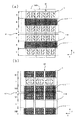
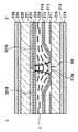
以下、図1〜図5を参照しながら本発明の第1実施形態に係る液晶表示装置について説明する。図1は本実施形態の液晶表示装置の概略構成を示す斜視図、図2はその要部平面図、図3はその要部断面図、図4はその作用を説明するための断面図、図5は液晶分子の配向状態を示す平面図である。なお、以下の各図においては、各層や各部材を図面上で認識可能な程度の大きさとするため、各層や各部材毎に縮尺を異ならせてある。また、本明細書では、液晶装置を構成する各部材において液晶層側に配置された面を「内面」、それと反対側の面を「外面」という。
本実施形態の液晶表示装置は単純マトリクス型の液晶表示装置であり、基板110,120には、それぞれ電極113,123がストライプ状に複数配列形成されている。電極113,123はそれぞれX方向、Y方向に延在して設けられ、これらの交差する略矩形の領域によって1つのドット領域が構成される。そして、このドット領域がマトリクス状に複数配列して画像表示領域が構成される。なお、図2において電極113間及び電極123間の領域をそれぞれ符号E1,E2で示しており、各ドット領域は平面視でこれらの領域E1,E2によって区画された状態となっている。
また、下基板110の外面側にはバックライト150が配置されている。
図3に示すように、下基板110とこれに対向配置された上基板120との間には、初期配向状態が垂直配向状態を呈する誘電異方性が負の液晶からなる液晶層130が挟持されている。
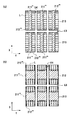
次に、図6,図7(a),(b)を参照しながら上記第1実施形態の変形例に係る液晶表示装置について説明する。図6,図7(a),(b)はそれぞれ上記第1実施形態の第1変形例,第2変形例,第3変形例に係る液晶表示装置における液晶の配向状態を示す平面図であり、図5に対応する図である。これらの変形例は、上記第1実施形態において反射膜及び液晶層厚調整層の配置を変形したものである。なお、本変形例において上記第1実施形態と同様の部材については同じ符号を付し、その説明を省略する。
図6(a)に示すように、本変形例では、反射膜111′はX方向に延在して設けられるとともにY方向に複数配列形成されている。この反射膜111′のY方向の幅は、透過表示領域Tと反射表示領域Rの開口比率に応じて任意に設定できるが、本変形例では例えば上電極123のY方向の幅の半分程度に設定されている。
これ以外は上記第1実施形態と同様である。
本変形例では、反射膜111′′′は下電極113の中央部にY方向に延在して設けられるとともにX方向に複数配列形成されている。この反射膜111′′′のX方向の幅は例えば下電極113のX方向の幅の半分程度に設定されている。これにより、1ドット領域内には、下電極113のX方向における両側部に2つの透過表示領域Tが形成され、下電極113のX方向における中央部に1つの反射表示領域Rが形成される。
これ以外は上記第1実施形態と同様である。
本変形例では、反射膜111′′′は下電極113の上下端部にY方向に延在して設けられるとともにX方向に複数配列形成されている。この反射膜111′′′のX方向の幅は例えば下電極113のX方向の幅の半分程度に設定されている。これにより、1ドット領域内には、下電極113のX方向における両側部に2つの反射表示領域R1、R2が形成され、下電極113のX方向における中央部に1つの透過表示領域Tが形成される。
これ以外は上記第1実施形態と同様である。
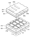
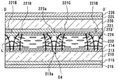
次に、図8〜図10を参照しながら本発明の第2実施形態に係る液晶表示装置について説明する。図8は本実施形態の液晶表示装置の概略構成を示す斜視図、図9はその要部断面図、図10は液晶分子の配向状態を示す平面図である。
本実施形態の液晶表示装置はアクティブマトリクス型の液晶表示装置であり、TFTアレイ基板である下基板210には略矩形の画素電極213が形成されており、これに対向基板である上基板220には共通電極223が形成されている。画素電極213は下基板210上にマトリクス状に複数配列形成されており、各画素電極213の形成領域がそれぞれドット領域を構成する。そして、このドット領域がマトリクス状に配列して画像表示領域が構成される。なお、図8において画素電極の形成されない領域(画素間領域)の内、X方向(画素電極213の短辺方向)に延在する画素間領域を符号E3で示し、Y方向(画素電極213の長辺方向)に延在する画素間領域を符号E4で示している。
また、下基板210の外面側にはバックライト250が配置されている。
図9に示すように、下基板210とこれに対向配置された上基板220との間には、初期配向状態が垂直配向状態を呈する誘電異方性が負の液晶からなる液晶層230が挟持されている。
そして、絶縁膜212の表面を含む基板210の表面には、ITO等の透明導電膜からなる画素電極213と垂直配向膜214とが順次形成されている。
なお、本実施形態では、下基板210がTFTアレイ基板として構成されるが、図9では、スイッチング素子としてのTFTや各種配線についての図示は省略している。
すなわち、領域E4を挟んでY方向に隣接する2つのドット領域からなるグループ領域内の透過表示領域T及び反射表示領域Rは共に配向分割された状態となる。同様に、領域E3を挟んでX方向に隣接する2つのドット領域からなるグループ領域内の透過表示領域T及び反射表示領域Rも共に配向分割された状態となる。
次に、図11〜図18を参照しながら上記第2実施形態の変形例に係る液晶表示装置について説明する。なお、本変形例において上記第2実施形態と同様の部材については同じ符号を付し、その説明を省略する。
これ以外は上記第2実施形態と同様である。
このような構成であっても上記第2実施形態と同様の効果が得られる。
これ以外は上記第2実施形態と同様である。
これ以外は上記第2実施形態と同様である。
これ以外は上記第2実施形態と同様である。
この構成では、1ドット領域内に液晶の傾倒方向の異なる2つのドメインが形成されることで配向分割が実現される。このため、本変形例では上記第2実施形態よりも一層広視野角な表示が得られる。
これ以外は上記第2実施形態と同様である。
この構成では、反射領域R、及び透過領域Tにおいて1ドット領域内に液晶の傾倒方向の異なる2つのドメインが形成されることで配向分割が実現される。このため、本変形例では上記第2実施形態よりも一層広視野角な表示が得られる。
これ以外は上記第2実施形態と同様である。
この構成では、1ドット領域内に傾倒方向の異なる4つのドメインが形成されることで配向分割が実現される。このため、本変形例では上記第2実施形態よりも一層広視野角な表示が得られる。
これ以外は上記第2実施形態と同様である。
この構成では、1ドット領域内に傾倒方向の異なる4つのドメインが形成されることで配向分割が実現される。このため、本変形例では上記第2実施形態よりも一層広視野角な表示が得られる。
また、上述の構成では共通電極に開口部223aを設けたが、この代わりに、上記開口部223aの位置に図19に示すような突起223bを設けてもよい。この構成でも同様の効果が得られる。
次に、本発明の上記実施の形態の液晶表示装置を備えた電子機器の具体例について説明する。
図20は、携帯電話の一例を示した斜視図である。図20において、符号500は携帯電話本体を示し、符号501は上記液晶表示装置を用いた表示部を示している。
図20に示す電子機器は、上記実施の形態の液晶表示装置を用いた表示部を備えているので、使用環境によらずに明るく、コントラストが高く、広視野角の液晶表示部を備えた電子機器を実現することができる。
例えば、上記実施形態及び変形例では、位相差板を単板で構成したが、この代わりに、1/2波長板と1/4波長板との積層体として構成してもよい。この積層体は広帯域円偏光板として機能し、黒表示をより無彩色化できる。さらに、この積層体に負のCプレートを積層させることで更に広視野角化を図ることもできる。なお、Cプレートとは膜厚方向に光軸を有する位相差板である。
Claims (10)
- 初期配向状態が垂直配向を呈する誘電異方性が負の液晶からなる液晶層を一対の基板間に挟持してなり、画像表示領域内に複数配列形成された1つのドット領域内に、透過表示を行なう透過表示領域と反射表示を行なう反射表示領域とが設けられた液晶表示装置であって、
隣接する2つのドット領域の透過表示領域同士又は反射表示領域同士がそれぞれそのドット領域の端辺に面する位置に設けられ、電圧印加時に各端辺に生じる斜め電界によって液晶が互いに逆向きに傾斜配向されることを特徴とする、液晶表示装置。 - 初期配向状態が垂直配向を呈する誘電異方性が負の液晶からなる液晶層を一対の基板間に挟持してなり、画像表示領域内に複数配列形成された1つのドット領域内に、透過表示を行なう透過表示領域と反射表示を行なう反射表示領域とが設けられた液晶表示装置であって、
隣接する2つのドット領域の透過表示領域同士又は反射表示領域同士がこれらのドット領域間の領域を挟んで対置されたことを特徴とする、液晶表示装置。 - 初期配向状態が垂直配向を呈する誘電異方性が負の液晶からなる液晶層を一対の基板間に挟持してなり、画像表示領域内に複数配列形成された1つのドット領域内に、透過表示を行なう透過表示領域と反射表示を行なう反射表示領域とが設けられた液晶表示装置であって、
隣接する2つのドット領域の透過表示領域同士又は反射表示領域同士が、これらのドット領域の隣接する方向に対して左側及び右側となる位置に対向して設けられたことを特徴とする、液晶表示装置。 - 前記一対の基板のうちの少なくとも一方の基板と前記液晶層との間には、前記反射表示領域と前記透過表示領域とで前記液晶層の層厚を異ならせる液晶層厚調整層が少なくとも前記反射表示領域に設けられたことを特徴とする、請求項1〜3のいずれかの項に記載の液晶表示装置。
- 前記ドット領域が略矩形に構成され、
前記透過表示領域が前記ドット領域の長辺に沿って配置されたことを特徴とする、請求項1〜4のいずれかの項に記載の液晶表示装置。 - 前記液晶層厚調整層が略矩形のドット領域の3つの端辺に沿って平面視コ字形に設けられ、前記透過表示領域が残りの1つの端辺に沿って配置されたことを特徴とする、請求項5記載の液晶表示装置。
- 前記透過領域が矩形状のドット領域の3つの端辺に沿って平面視コ字形に設けられ、前記液晶層厚調整層が残りの1つの端辺に沿って配置されたことを特徴とする、請求項5記載の液晶表示装置。
- 前記透過表示領域が略矩形のドット領域の4つの端辺に沿って4箇所設けられたことを特徴とする、請求項5記載の液晶表示装置。
- 前期液晶層厚調整層が矩形状のドット領域の4つの端辺に沿って4箇所設けられたことを特徴とする、請求項5記載の液晶表示装置。
- 請求項1〜9のいずれかの項に記載の液晶表示装置を備えたことを特徴とする、電子機器。
Priority Applications (5)
| Application Number | Priority Date | Filing Date | Title |
|---|---|---|---|
| JP2004031060A JP3944649B2 (ja) | 2003-04-21 | 2004-02-06 | 液晶表示装置および電子機器 |
| US10/808,565 US7126658B2 (en) | 2003-04-21 | 2004-03-25 | Liquid crystal display device and electronic apparatus having particular dot regions |
| TW093109762A TW200510824A (en) | 2003-04-21 | 2004-04-08 | Liquid crystal display and its electronic equipment |
| KR1020040027560A KR100743743B1 (ko) | 2003-04-21 | 2004-04-21 | 액정 표시 장치 및 전자 기기 |
| CNB2004100327823A CN1282020C (zh) | 2003-04-21 | 2004-04-21 | 液晶显示装置以及电子设备 |
Applications Claiming Priority (2)
| Application Number | Priority Date | Filing Date | Title |
|---|---|---|---|
| JP2003116364 | 2003-04-21 | ||
| JP2004031060A JP3944649B2 (ja) | 2003-04-21 | 2004-02-06 | 液晶表示装置および電子機器 |
Publications (2)
| Publication Number | Publication Date |
|---|---|
| JP2004341486A true JP2004341486A (ja) | 2004-12-02 |
| JP3944649B2 JP3944649B2 (ja) | 2007-07-11 |
Family
ID=33312615
Family Applications (1)
| Application Number | Title | Priority Date | Filing Date |
|---|---|---|---|
| JP2004031060A Expired - Lifetime JP3944649B2 (ja) | 2003-04-21 | 2004-02-06 | 液晶表示装置および電子機器 |
Country Status (5)
| Country | Link |
|---|---|
| US (1) | US7126658B2 (ja) |
| JP (1) | JP3944649B2 (ja) |
| KR (1) | KR100743743B1 (ja) |
| CN (1) | CN1282020C (ja) |
| TW (1) | TW200510824A (ja) |
Cited By (4)
| Publication number | Priority date | Publication date | Assignee | Title |
|---|---|---|---|---|
| JP2007052267A (ja) * | 2005-08-18 | 2007-03-01 | Toshiba Matsushita Display Technology Co Ltd | 液晶表示装置 |
| JP2007121643A (ja) * | 2005-10-27 | 2007-05-17 | Toshiba Matsushita Display Technology Co Ltd | 液晶表示装置 |
| JP2007140435A (ja) * | 2005-11-17 | 2007-06-07 | Toppoly Optoelectronics Corp | 薄膜トランジスタアレイ、半透過型薄膜トランジスタ液晶ディスプレイ、lcdデバイス及び電子デバイス |
| JP2009075179A (ja) * | 2007-09-19 | 2009-04-09 | Hitachi Displays Ltd | 液晶表示装置 |
Families Citing this family (11)
| Publication number | Priority date | Publication date | Assignee | Title |
|---|---|---|---|---|
| TWI315010B (en) * | 2003-03-31 | 2009-09-21 | Sharp Corporatio | Liquid crystal display device and method of manufacturing the same |
| JP2006091059A (ja) * | 2004-09-21 | 2006-04-06 | Seiko Epson Corp | 電気光学装置、電気光学装置の製造方法、及び電子機器 |
| JP4337794B2 (ja) * | 2005-09-16 | 2009-09-30 | エプソンイメージングデバイス株式会社 | 液晶装置および電子機器 |
| CN100526947C (zh) * | 2006-11-15 | 2009-08-12 | 胜华科技股份有限公司 | 液晶显示面板及应用其的液晶显示装置 |
| US8089590B2 (en) * | 2007-08-06 | 2012-01-03 | Chimei Innolux Corporation | Transflective liquid crystal display |
| GB0909422D0 (en) * | 2009-06-02 | 2009-07-15 | Cambridge Entpr Ltd | Electro-Optical Switching Device |
| WO2011065362A1 (ja) * | 2009-11-27 | 2011-06-03 | シャープ株式会社 | 半導体装置およびその製造方法 |
| CN110967854A (zh) * | 2018-09-28 | 2020-04-07 | 夏普株式会社 | 液晶面板 |
| CN109799641B (zh) * | 2019-03-29 | 2021-10-22 | 合肥京东方光电科技有限公司 | 一种阵列基板及其制备方法、液晶显示面板 |
| JP6763620B1 (ja) * | 2019-06-04 | 2020-09-30 | 株式会社トヨックス | 可撓管及びその製造方法 |
| JP2023163521A (ja) * | 2022-04-28 | 2023-11-10 | シャープディスプレイテクノロジー株式会社 | 液晶表示装置 |
Family Cites Families (14)
| Publication number | Priority date | Publication date | Assignee | Title |
|---|---|---|---|---|
| JP3234357B2 (ja) | 1993-07-08 | 2001-12-04 | 三洋電機株式会社 | 液晶表示装置 |
| TW589504B (en) | 1997-06-12 | 2004-06-01 | Sharp Kk | Liquid crystal display device |
| JP3380482B2 (ja) * | 1997-12-26 | 2003-02-24 | シャープ株式会社 | 液晶表示装置 |
| KR100471012B1 (ko) * | 1998-02-04 | 2005-03-07 | 세이코 엡슨 가부시키가이샤 | 액정장치 및 전자기기 |
| JP3610264B2 (ja) | 1999-08-03 | 2005-01-12 | シャープ株式会社 | 液晶表示素子 |
| TW548475B (en) | 1999-11-18 | 2003-08-21 | Ind Tech Res Inst | Fabrication method of homeotropic aligned LCD structure and the bump structure |
| JP3665263B2 (ja) * | 2000-01-18 | 2005-06-29 | シャープ株式会社 | 液晶表示装置 |
| US6924876B2 (en) * | 2000-02-25 | 2005-08-02 | Sharp Kabushiki Kaisha | Liquid crystal display device |
| KR20020015228A (ko) | 2000-08-21 | 2002-02-27 | 구본준, 론 위라하디락사 | 반사투과형 액정표시장치용 어레이기판과 그 제조방법 |
| JP2002075839A (ja) | 2000-08-30 | 2002-03-15 | Canon Inc | 露光装置、該露光装置に用いるマスク構造体、露光方法、該露光装置を用いて作製された半導体デバイス、および半導体デバイス製造方法 |
| TW571165B (en) * | 2000-12-15 | 2004-01-11 | Nec Lcd Technologies Ltd | Liquid crystal display device |
| JP2002287158A (ja) | 2000-12-15 | 2002-10-03 | Nec Corp | 液晶表示装置およびその製造方法ならびに駆動方法 |
| JP3767419B2 (ja) * | 2001-05-28 | 2006-04-19 | ソニー株式会社 | 液晶表示素子 |
| JP2003215591A (ja) * | 2002-01-25 | 2003-07-30 | Alps Electric Co Ltd | 半透過反射型液晶表示装置 |
-
2004
- 2004-02-06 JP JP2004031060A patent/JP3944649B2/ja not_active Expired - Lifetime
- 2004-03-25 US US10/808,565 patent/US7126658B2/en not_active Expired - Lifetime
- 2004-04-08 TW TW093109762A patent/TW200510824A/zh not_active IP Right Cessation
- 2004-04-21 CN CNB2004100327823A patent/CN1282020C/zh not_active Expired - Lifetime
- 2004-04-21 KR KR1020040027560A patent/KR100743743B1/ko not_active Expired - Lifetime
Cited By (4)
| Publication number | Priority date | Publication date | Assignee | Title |
|---|---|---|---|---|
| JP2007052267A (ja) * | 2005-08-18 | 2007-03-01 | Toshiba Matsushita Display Technology Co Ltd | 液晶表示装置 |
| JP2007121643A (ja) * | 2005-10-27 | 2007-05-17 | Toshiba Matsushita Display Technology Co Ltd | 液晶表示装置 |
| JP2007140435A (ja) * | 2005-11-17 | 2007-06-07 | Toppoly Optoelectronics Corp | 薄膜トランジスタアレイ、半透過型薄膜トランジスタ液晶ディスプレイ、lcdデバイス及び電子デバイス |
| JP2009075179A (ja) * | 2007-09-19 | 2009-04-09 | Hitachi Displays Ltd | 液晶表示装置 |
Also Published As
| Publication number | Publication date |
|---|---|
| KR100743743B1 (ko) | 2007-07-27 |
| TWI294982B (ja) | 2008-03-21 |
| CN1282020C (zh) | 2006-10-25 |
| US20040218122A1 (en) | 2004-11-04 |
| JP3944649B2 (ja) | 2007-07-11 |
| US7126658B2 (en) | 2006-10-24 |
| KR20040091588A (ko) | 2004-10-28 |
| TW200510824A (en) | 2005-03-16 |
| CN1540419A (zh) | 2004-10-27 |
Similar Documents
| Publication | Publication Date | Title |
|---|---|---|
| JP4123208B2 (ja) | 液晶表示装置、電子機器 | |
| JP3807405B2 (ja) | 液晶表示装置、及び電子機器 | |
| CN1573428B (zh) | 液晶显示装置以及电子设备 | |
| JP2005173037A (ja) | 液晶表示装置及びその製造方法 | |
| JP4093217B2 (ja) | 液晶表示装置および電子機器 | |
| JP3900141B2 (ja) | 液晶表示装置および電子機器 | |
| US7995169B2 (en) | Liquid crystal display device and electronic apparatus | |
| JP3944649B2 (ja) | 液晶表示装置および電子機器 | |
| JP4337794B2 (ja) | 液晶装置および電子機器 | |
| JP2004333700A (ja) | 液晶表示装置及び電子機器 | |
| JP3807375B2 (ja) | 液晶表示装置および電子機器 | |
| JP3901172B2 (ja) | 液晶表示装置および電子機器 | |
| JP4449335B2 (ja) | 液晶表示装置および電子機器 | |
| JP4432371B2 (ja) | 液晶表示装置、及び電子機器 | |
| JP4766037B2 (ja) | 液晶表示装置、電子機器 | |
| JP3903980B2 (ja) | 液晶表示装置および電子機器 | |
| JP4385908B2 (ja) | 液晶表示装置、液晶表示装置の駆動方法および電子機器 | |
| JP4525259B2 (ja) | 液晶表示装置および電子機器 | |
| JP4314906B2 (ja) | 液晶表示装置および電子機器 | |
| JP2005128233A (ja) | 液晶表示装置および電子機器 | |
| JP5376417B2 (ja) | 半透過型液晶表示パネル | |
| JP2007072149A (ja) | 液晶装置および電子機器 | |
| JP2008233137A (ja) | 液晶表示装置 | |
| JP4249776B2 (ja) | 液晶表示装置、及び電子機器 |
Legal Events
| Date | Code | Title | Description |
|---|---|---|---|
| A977 | Report on retrieval |
Free format text: JAPANESE INTERMEDIATE CODE: A971007 Effective date: 20060201 |
|
| A131 | Notification of reasons for refusal |
Free format text: JAPANESE INTERMEDIATE CODE: A131 Effective date: 20060627 |
|
| A521 | Request for written amendment filed |
Free format text: JAPANESE INTERMEDIATE CODE: A523 Effective date: 20060824 |
|
| A131 | Notification of reasons for refusal |
Free format text: JAPANESE INTERMEDIATE CODE: A131 Effective date: 20061017 |
|
| A521 | Request for written amendment filed |
Free format text: JAPANESE INTERMEDIATE CODE: A523 Effective date: 20061214 |
|
| TRDD | Decision of grant or rejection written | ||
| A01 | Written decision to grant a patent or to grant a registration (utility model) |
Free format text: JAPANESE INTERMEDIATE CODE: A01 Effective date: 20070313 |
|
| RD04 | Notification of resignation of power of attorney |
Free format text: JAPANESE INTERMEDIATE CODE: A7424 Effective date: 20070403 |
|
| A61 | First payment of annual fees (during grant procedure) |
Free format text: JAPANESE INTERMEDIATE CODE: A61 Effective date: 20070326 |
|
| R150 | Certificate of patent or registration of utility model |
Ref document number: 3944649 Country of ref document: JP Free format text: JAPANESE INTERMEDIATE CODE: R150 Free format text: JAPANESE INTERMEDIATE CODE: R150 |
|
| FPAY | Renewal fee payment (event date is renewal date of database) |
Free format text: PAYMENT UNTIL: 20110420 Year of fee payment: 4 |
|
| FPAY | Renewal fee payment (event date is renewal date of database) |
Free format text: PAYMENT UNTIL: 20110420 Year of fee payment: 4 |
|
| FPAY | Renewal fee payment (event date is renewal date of database) |
Free format text: PAYMENT UNTIL: 20120420 Year of fee payment: 5 |
|
| FPAY | Renewal fee payment (event date is renewal date of database) |
Free format text: PAYMENT UNTIL: 20130420 Year of fee payment: 6 |
|
| FPAY | Renewal fee payment (event date is renewal date of database) |
Free format text: PAYMENT UNTIL: 20130420 Year of fee payment: 6 |
|
| FPAY | Renewal fee payment (event date is renewal date of database) |
Free format text: PAYMENT UNTIL: 20140420 Year of fee payment: 7 |
|
| S111 | Request for change of ownership or part of ownership |
Free format text: JAPANESE INTERMEDIATE CODE: R313113 |
|
| S111 | Request for change of ownership or part of ownership |
Free format text: JAPANESE INTERMEDIATE CODE: R313113 |
|
| R371 | Transfer withdrawn |
Free format text: JAPANESE INTERMEDIATE CODE: R371 |
|
| S111 | Request for change of ownership or part of ownership |
Free format text: JAPANESE INTERMEDIATE CODE: R313113 |
|
| R350 | Written notification of registration of transfer |
Free format text: JAPANESE INTERMEDIATE CODE: R350 |
|
| R250 | Receipt of annual fees |
Free format text: JAPANESE INTERMEDIATE CODE: R250 |
|
| R250 | Receipt of annual fees |
Free format text: JAPANESE INTERMEDIATE CODE: R250 |
|
| R250 | Receipt of annual fees |
Free format text: JAPANESE INTERMEDIATE CODE: R250 |
|
| R250 | Receipt of annual fees |
Free format text: JAPANESE INTERMEDIATE CODE: R250 |
|
| R250 | Receipt of annual fees |
Free format text: JAPANESE INTERMEDIATE CODE: R250 |
|
| R250 | Receipt of annual fees |
Free format text: JAPANESE INTERMEDIATE CODE: R250 |
|
| R250 | Receipt of annual fees |
Free format text: JAPANESE INTERMEDIATE CODE: R250 |
|
| R250 | Receipt of annual fees |
Free format text: JAPANESE INTERMEDIATE CODE: R250 |
|
| EXPY | Cancellation because of completion of term |