JP2004349632A - Board mounting structure, board mounting method and mounted components - Google Patents
Board mounting structure, board mounting method and mounted components Download PDFInfo
- Publication number
- JP2004349632A JP2004349632A JP2003147870A JP2003147870A JP2004349632A JP 2004349632 A JP2004349632 A JP 2004349632A JP 2003147870 A JP2003147870 A JP 2003147870A JP 2003147870 A JP2003147870 A JP 2003147870A JP 2004349632 A JP2004349632 A JP 2004349632A
- Authority
- JP
- Japan
- Prior art keywords
- hole
- mounting structure
- pin
- board mounting
- insertion portion
- Prior art date
- Legal status (The legal status is an assumption and is not a legal conclusion. Google has not performed a legal analysis and makes no representation as to the accuracy of the status listed.)
- Pending
Links
Images









Landscapes
- Coupling Device And Connection With Printed Circuit (AREA)
- Electric Connection Of Electric Components To Printed Circuits (AREA)
- Structures For Mounting Electric Components On Printed Circuit Boards (AREA)
- Multi-Conductor Connections (AREA)
Abstract
【課題】接続ピンにスルーホールの内径よりも小さな外径を有する挿入部を設け、スルーホールに挿入された挿入部を拡張することにより実装部品を基板に装着する基板実装構造の提供。
【解決手段】基板1に設けられたスルーホール4に実装部品2の挿入ピンを挿入して、スルーホール4に露出したメッキ層7と挿入ピン3とを接続する基板実装構造に関する。挿入ピン3にはスルーホールの内径よりも小さな外径を有する小径部31が形成されており、その小径部3をスルーホール4に挿入した後に、小径部31を固定ピン10を挿入して拡張する。その結果、挿入ピン3の外周面がスルーホール4の内周面に押圧され、接続ピンと基板との電気的接続および機械的固定が行われる。
【選択図】 図3Provided is a board mounting structure in which an insertion portion having an outer diameter smaller than the inner diameter of a through hole is provided in a connection pin, and a mounting component is mounted on a substrate by expanding the insertion portion inserted into the through hole.
The present invention relates to a board mounting structure in which an insertion pin of a mounting component (2) is inserted into a through hole (4) provided in a substrate (1) and a plating layer (7) exposed in the through hole (4) is connected to the insertion pin (3). The insertion pin 3 has a small diameter portion 31 having an outer diameter smaller than the inner diameter of the through hole. After the small diameter portion 3 is inserted into the through hole 4, the small diameter portion 31 is expanded by inserting the fixing pin 10. I do. As a result, the outer peripheral surface of the insertion pin 3 is pressed against the inner peripheral surface of the through-hole 4, so that electrical connection and mechanical fixing between the connection pin and the substrate are performed.
[Selection diagram] FIG.
Description
【0001】
【発明の属する技術分野】
本発明は、基板に設けられたスルーホールに実装部品の接続ピンを挿入して、実装部品を基板に装着する基板実装構造、基板実装方法、および、それらに用いられる実装部品に関する。
【0002】
【従来の技術】
プリント基板に電子部品を実装する方法の一つに、プレスフィット工法と呼ばれるものが知られている。プレスフィット工法におけるコネクタピンには、プレスフィット部やコンプライアンス部などと呼ばれるスルーホールの内径よりも径の大きな部分が形成されている。コネクタピンをスルーホールに圧入するとプレスフィット部が弾性変形し、そのときの接触圧力によりピンとプリント基板導体との電気的接続や機械的な固定が行われる(例えば、特許文献1および特許文献2参照。)。
【0003】
【特許文献1】
特開平6−13735号公報
【特許文献2】
特開平10−92999号公報
【0004】
【発明が解決しようとする課題】
スルーホール内壁表面にはメッキ層が薄く形成されていて、このメッキ層とコネクタピンとが接触してプリント基板導体との導通がとられている。しかしながら、プレスフィット工法ではスルーホール内径よりも大径のコネクタピンがスルーホールに圧入されるため、圧入時に摩擦によってスルーホール内のメッキが剥離する等のメッキ層へのダメージが生じて、導通不良につながる可能性があった。
【0005】
本発明は、接続ピンにスルーホールの内径よりも小さな外径を有する挿入部を設け、スルーホールに挿入された挿入部を拡張することにより実装部品を基板に装着する基板実装構造、基板実装方法、および、それらに用いられる実装部品を提供するものである。
【0006】
【課題を解決するための手段】
本発明は、基板に設けられたスルーホールに実装部品の接続ピンを挿入して、前記スルーホールに露出した前記基板の導通部と前記接続ピンとを接続する基板実装構造や基板実装方法に適用されるものである。そして、接続ピンに形成されたスルーホールの内径よりも小さな外径を有する挿入部をスルーホールに挿入し、その後に、挿入部を拡張手段で拡張して挿入部の外周面がスルーホールの内周面に押圧されるようにし、接続ピンと基板との電気的接続および機械的固定を行うようにしたことを特徴とする。
また、本発明による実装部品では、接続ピンにスルーホールの内径よりも小さな外径を有する挿入部が形成され、挿入部は柱状体の拡張手段が挿入される中空部を有する筒状体状に形成されている。
【0007】
【発明の効果】
本発明によれば、接続ピンにスルーホールの内径よりも小さな外径を有する挿入部を形成し、その挿入部をスルーホールに挿入してから拡張するようにしたので、スルーホール内壁にメッキ等により形成された導通部が接続ピンの挿入によってダメージを受けるのを防止することができる。
【0008】
【発明の実施の形態】
以下、図を参照して本発明の実施の形態を説明する。図1は本発明による実装構造の一実施の形態を説明する図であり、実装前の挿入型実装部品2および基板1の断面図を示したものである。実装部品2に設けられた接続端子としての挿入ピン3は、基板1のスルーホール4に挿入される。実装部品2としては、コネクタや、樹脂によりパッケージングされたICなどの電子部品や、ICを基板に実装するためのソケット等がある。なお、実装部品2には複数の挿入ピン3が設けられていて各々スルーホール4に挿入されているが、図1は、それらの内の一カ所について図示したものである。
【0009】
基板1は複数の配線層5a,5bが積層された多層基板であり、各配線層5a,5bは絶縁性の基板基材6により互いに絶縁されている。図1の例では2層の配線層5a,5bを有しているが、本発明は配線層の数に関係なく適用することができる。スルーホール4には導電性材料によるメッキ層7が形成されている。メッキ層7には例えば銅メッキなどが用いられ、メッキ層7の一部はスルーホール4から連続するように基板1の表裏面に露出している。メッキ層7は、スルーホール4内に露出している配線層5a,5bを覆うように形成されており、配線層5a,5bと電気的に接続されている。
【0010】
挿入ピン3は、外径T1の小径部31、外径T2の大径部33およびフランジ状のストッパ部32から成る。図2は挿入ピン3の斜視図であり、挿入ピン3の中心部分には中空部8が形成されるている。また、筒状の挿入ピン3には、スリット9が軸方向に沿ってピン先端から実装部品方向へと形成されている。図2に示す例では、2つのスリット9が軸の回りに180度ずれた位置に設けられている。ストッパ部32の下面と大径部33の上面との間隔d1はスルーホール4の長さd2よりもやや大きく設定されている。また、大径部33の外径T2は小径部の外径T1よりも大きく設定されるが、スルーホール4の内径T5と同じまたはやや小さく設定されている。
【0011】
図1に示した実装部品2を基板1に実装する場合には、まず、図3(a)に示すように、ストッパ部32が基板1に当接するまで挿入ピン3を基板1のスルーホール4に挿入する。大径部33の外径T2はスルーホール4の内径T5と同じまたはやや小さく設定されているため、ピン挿入の際の軸の僅かなずれによってメッキ層7の表面が大径部33によって擦られ、その際にメッキ層7が僅かに削り取られる。メッキ層7の表面には酸化膜が出来やすく、酸化膜によって導通抵抗にばらつきが生じやすい。しかしながら、本実施の形態ではスルーホール4の内表面に形成された酸化膜が大径部33によって削りとられる場合が多く、酸化膜による導通抵抗のばらつきを防止することができる。
【0012】
上述したように、スルーホール4の内径T5は「T5>T1」のように設定されているので、図3(a)に示す状態ではスルーホール4と挿入ピン3の小径部31との間には隙間が生じている。次に、図3(b)に示すように、固定ピン10を挿入ピン3の先端から実装部品方向に押圧して、中空部8に固定ピン10を挿入する。固定ピン10は挿入部101と大径部102とを有しており、挿入部101の外径はT4であって、その先端部分は砲弾の先端部のように先端に近づくほど細くなっている。挿入部101の外径T4は中空部8の内径T3よりも大きく設定されており、固定ピン10を中空部8に挿入すると、挿入ピン3が図3(b)の矢印11で示す左右方向に変形される。挿入ピン3に形成されたスリット9は、このときの変形が生じやすいように機能している。
【0013】
そのため、固定ピン10の挿入開始によって挿入ピン3の大径部33がスルーホール4の入り口部分に引っ掛かり、固定ピン10の上方への押圧力による挿入ピン3のスルーホール4からの抜けが防止される。さらに、図4(a)に示すように固定ピン10を中空部8に挿入することにより挿入ピン3が押し広げられ、挿入ピン3の外径が増加するように拡張される。その結果、挿入ピン3の外周面がスルーホール4の内周面に押圧され、挿入ピン3とスルーホール4との電気的接続が十分に行われるとともに、挿入ピン3がスルーホール4に固定される。
【0014】
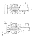
図4(a)は、固定ピン10の後端に形成された大径部102が挿入ピン3の先端に当接して、挿入部101の全体が中空部8に挿入された状態を示す断面図であり、図4(b)はII−II断面を示す図である。固定ピン10の外径T4は、次式(1)を満たすように設定されている。
【数1】
{(T1−T3)+T4}>T5 …(1)
【0015】
式(1)において、左辺は固定ピン10の外径T4に小径部31の肉厚部分を加えた外形寸法を表している。外径T4を式(1)のように設定することにより、小径部31の外周面をスルーホール4の内面に密着させるとともに、接触抵抗が小さくなるように十分な面圧が得られるようにしている。
【0016】
なお、図4(a)ではスリット9の上端部がストッパ32よりも実装部品側となるように十分長く設定されているため、固定ピン10の大径部102が挿入ピン3の先端に当接するまで挿入されている。しかし、図5に示すようにスリット9の長さがストッパ部32よりも上方まで形成されていないような場合には、固定ピン10が途中までしか挿入されないこともある。そのため、挿入ピン3が拡張したときの小径部31とスルーホール4との密着性を十分得るためには、スリット9の上端部がストッパ部32よりも実装部品側となるようにするのが好ましい。
【0017】
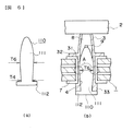
上述した固定ピン10では、挿入部101は先端部分を除いては外径T4の円柱状を成している。図6(a)は固定ピン10の変形例を示す図であり、固定ピン110は挿入部111と大径部112とを有している。図6(a)に示す固定ピン110では、挿入部111の基部付近の外径は固定ピン10と同じT4であるが、挿入部111の中央部付近の外径T6はT4よりも大きく設定されていて樽状に膨らんでいる。
【0018】
そのため、この固定ピン110を用いた場合には、図6(b)に示すように、符号Aで示した外径T6を有する部分において挿入ピン3の最大密着応力を発生させることができる。そのため、固定ピン110が挿入ピン3から抜け難くなるとともに、符号Aで示した部分を中心に挿入ピン3とスルーホール4との密着応力が固定ピン10を用いた場合よりも大きくなる。その結果、挿入ピン3と基板1との間の電気的接続および機械的固定がより良好となる。
【0019】
なお、固定ピン10,110には樹脂等の弾性を有する材料で形成するのが望ましい。固定ピン10,110を弾性材料で形成した場合、弾性によって挿入時におけるスルーホール4の入り口部分に与える広がり方向の応力を軽減できる。さらに、弾性材料で形成した場合には固定ピン10のような挿入部形状であっても、固定ピン挿入後にスルーホール4の中央部付近に挿入ピン3の最大密着応力を発生させることができ、固定ピンを抜け難くすることが出来る。また、固定ピン10,110の先端部形状は上述した形状に限らず、挿入ピン3の中空部8に挿入しやすい形状であれば良い。
【0020】
《挿入ピンの構造》
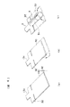
図3に示した挿入ピン3では、円柱状の金属部材を旋盤加工することによりストッパ部32および大径部33を形成したが、図7〜9に示すような方法で形成しても良い。図7(a)に示す例では、プレス加工等によりストッパ部32を有する部材13aを形成する。そして、部材13aのストッパ部2よりも先端部分を旋盤加工して、円柱状の小径部31と大径部33を形成した後に、ドリル加工により中空部8を形成する。最後に、スリット9を形成する。
【0021】
小径部31はスルーホール4との密着性が良好となるように、小径部31の断面形状はスルーホール4の断面と同様に円形が好ましい。そのため、部材13aの厚さt10は小径部31の外径T1以上に設定される。ただし、図7(a)に示す例ではt10は大径部33の外径T2よりも小さいので、大径部33およびストッパ部32とも断面は円形となっていない。しかし、これらは固定ピン10を挿入する際に基板1にかかる応力を受けることが出来れば良いので、必ずしも円形である必要はない。図7(b)の部材13bでは厚さt11がT2以上に設定されており、小径部31および大径部33を円柱状に形成することができる。
【0022】
なお、図7(a)に示した挿入ピン3ではスリット9の数が2つで、図7(b)に示した挿入ピンではスリット9が1つであるが、図7(c)の小径部31の断面図に示すようにスリット9の数は3つ以上でもかまわない。ただし、固定ピン10を中空部8に挿入したときの挿入ピン3の変形が軸対称となるように、複数のスリット9の配置は軸対称とするのが好ましい。なお、図7(a)に示す挿入ピン3では大径部33やストッパ部32の形状が左右対称なので、スリット9の数は2が好ましい。
【0023】
また、図8,9に示す例では、金属の薄板を曲げ加工して挿入ピン3を形成するようにしている。図8に示す例の場合、図8(a)のように薄板13cを図のようにストッパ部32を構成する部分と、小径部31および大径部33に相当する部分130とから成る形状に形成する。このときの薄板13cの厚さt12は、小径部31の肉厚と等しく設定される。図1からも分かるように、小径部31の肉厚は(T1−T3)/2となる。
【0024】
図8(b)では部分130の先端部を折り曲げて大径部33に相当するを形成する。次に、図8(c)のように、部分130を円筒状に丸めて小径部31と大径部33を形成する。部分130を丸め加工する際には、接合部にはスリット9を構成する隙間をあけるように丸める。このようにして、薄板13cから、ストッパ部32,小径部31,大径部33およびスリット9を有する円筒状の挿入ピン3が形成される。
【0025】
図9に示す挿入ピン3では、図9(a)に示すように、薄板13dはストッパ部32と小径部31に相当する部分131とを有している。部分131を図9(b)のように円筒状に丸め、その丸め加工の際に、スリット9ができるように接合部に隙間をあける。その結果、ストッパ部32と小径部31のみを有する挿入ピン3が形成される。
【0026】
図9(b)に示した挿入ピン3では、図1に示すような大径部33を有していないが、図7(a)に示すような金属材を削りだして形成する挿入ピン3においても、大径部33を形成しないようにすることができる。図10は、挿入ピン3に大径部33が無い場合の挿入ピン3と基板1との接続方法を示したものである。まず、図10(a)のように、挿入ピン3の小径部31を、ストッパ部32が基板1に当接するまでスルーホール4内に挿入する。
【0027】
次に、図10(b)のようにストッパ部32の上部を押さえ治具14で押さえながら、基板裏面側から固定ピン10を中空部8に挿入する。すなわち、固定ピン挿入時の挿入ピン3を上方に押し上げる力に対して、押さえ治具14によって挿入ピン3を下方に押さえつけることにより、小径部31がスルーホール4から抜け出てしまうのを防止している。なお、固定ピン10を挿入したときの挿入ピン3の外径方向への変形を考慮して、押さえ治具14と挿入ピン3との間には若干の隙間をあけておく。図10(c)に示すように固定ピン10の挿入が完了したならば、押さえ治具14を挿入ピン3から取り外す。
【0028】
さらに、図9に示した挿入ピン3の場合には、固定ピン10を挿入ピン3の先端側からではなく、実装部品側から挿入することもできる。図11は実装手順を示す図であり、図11に示すように基板1を定盤15上に置き、実装部品2に設けられた挿入ピン3を基板1のスルーホール4に挿入する。次に、図11(b)のように固定ピン10を実装部品側、すなわち、基板1の表面側から小径部31の中空部8に挿入する。固定ピン挿入の際の挿入方向の応力は、定盤15およびストッパ部32により受ける。
【0029】
なお、この方式の場合、固定ピン10の大径部102の形状を挿入ピン3と干渉しないような形状とする必要がある。例えば、ストッパ部32の延在方向に長い楕円形とする。その後、図11(c)に示すように固定ピン10を押し込むことによって挿入ピン3が外径方向に拡張し、挿入ピン3が基板1に固定される。
【0030】
[変形例1]
図12は固定ピン10の挿入方法に関する変形例であり、固定ピン10をねじ込むように回転させながら挿入ピン3の中空部8に挿入する。この場合、矢印R1のように回転方向を正逆両方向に僅かに反転させながら挿入する。そうすると、挿入ピン3は固定ピン10から上方方向の力を受けているため、挿入ピン3と固定ピン10との間の摩擦力によって挿入ピン3も矢印R2のように連れ回ることになる。
【0031】
固定ピン10の挿入過程において図12(b)のように固定ピンの挿入量が増えると、挿入ピン3が外径方向に変形してスルーホール4の内面、すなわちメッキ層7の内表面に接触する。そして、接触しながら挿入ピン3が連れ回ることによりメッキ層7の表面の酸化膜が削り取られ、挿入ピン3とメッキ層7との密着力が向上して電気的接続状態がより良好になる。
【0032】
[変形例2]
図13は変形例2を示す図であり、図13(a)に示すように小径部31の表面を予め凹凸状に粗面化しておく。その結果、図13(b)のように固定ピン10を挿入して挿入ピン31を変形させ、小径部31の外面とスルーホール4の内面とが密着したときに、両者の間の固定力がより増加する。
【0033】
[変形例3]
変形例3では、基板1、挿入ピン3および固定ピン10の内で、固定ピン10に用いられる材料の熱膨張係数を基板1,挿入ピン3の材料よりも大きくした。実装部品2の発熱等により実装部品2を含む基板1の温度が上昇した場合、上述したように固定ピン10の熱膨張係数を他のものよりも大きくしておくことにより、固定ピン10の熱膨張により挿入ピン3とスルーホール4との密着力が増加し、接続部の耐久性が向上する。なお、固定ピン6の外径T4は、低温時に固定ピン10が収縮した場合でも、挿入ピン3とスルーホール4との密着力が維持出来るような大きさに設定しておく。
【0034】
[変形例4]
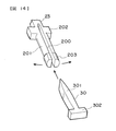
上述した実施の形態では、中空部8を有する円筒状の挿入ピン3にスリット9を形成し、挿入ピン3の中空部8に先端が細くなった円柱状の固定ピンを挿入することにより、挿入ピン3を外径方向に変形させて挿入ピン3をスルーホール4に固定するようにしていた。変形例4では、図14のように割り込み200を有する挿入ピン23を図1の基板1のスルーホール4に挿入し、その挿入ピン23の割り込み200に楔状の固定ピン30を圧入するようにしても良い。
【0035】
この場合も、挿入ピン23には小径部201,ストッパ部202および大径部203が形成されており、小径部201の断面形状はスルーホール4の断面形状に合わせて円形とされる。図14に示す固定ピン30は板状部材から成り、楔部301の後端には固定ピン30の挿入量を制限するストッパ部302が形成されている。
【0036】
[変形例5]
上述した実施の形態では、固定ピン10が複数ある場合には、それぞれの固定ピン10を対応する挿入ピン3に個別に挿入される。しかし、固定ピン10を絶縁性の樹脂で形成する場合には、図15に示すように複数の固定ピン401が一体に形成された固定ピンユニット40を用いて、複数の挿入ピン3をいっぺんに基板1に接続固定することができる。固定ピンユニット40は複数の固定ピン10が連結部402で連結されたものであり、一体で成形される。固定ピン401には固定ピン10に設けられていたような大径部33は形成されていないが、連結部402が大径部33と同一の機能を有している。各固定ピン401の間隔d10は基板1に形成されたスルーホール4の間隔と等しく設定されている。実装部品2に形成されている挿入ピン3の構造は、図1に示したものと同一である。
【0037】
実装部品2を基板1に実装する場合には、図16(a)に示すように、実装部品2に設けられた複数の挿入ピン3を基板1の対応するスルーホール4に挿入する。そして、固定ピンユニット40の全体を基板方向に移動させて、各固定ピン401を挿入ピン3の中空部8に挿入する。固定ピン挿入時の挿入ピン3の変形等については図3で説明した動作と同一なので、ここでは説明を省略する。図16(b)は各固定ピン401が完全に挿入された状態を示す図であり、連結部402は各挿入ピン3の大径部33に当接している。
【0038】
このように複数の固定ピン401が形成された固定ピンユニット40を用いることにより、複数の固定ピン401を挿入ピン3にいっぺんに挿入することができるため、作業効率の向上を図ることが出来る。なお、固定ピンユニット40は絶縁性樹脂で形成されているので、固定ピン401同士が連結部402で連結されていても、スルーホール4同士が固定ピンユニット40を介して導通することはない。
【0039】
図16に示す固定ピンユニット40では固定ピン401と連結部402とを樹脂で一体に形成したが、図17に示すように、複数の金属製のピン411を樹脂製の連結部材412で連結した固定ピンユニット41を用いてもより。固定ピン411の下端部414は連結部材412に形成された孔413に挿入されている。
【0040】
以上説明した実施の形態と特許請求の範囲の要素との対応において、メッキ層7は導通部を、小径部31は挿入部を、固定ピン10は拡張手段を、大径部33は突出部を、固定ピン401,411は請求項6の柱状体をそれぞれ構成している。また、本発明の特徴を損なわない限り、本発明は上記実施の形態に何ら限定されるものではない。
【図面の簡単な説明】
【図1】本発明による実装構造の一実施の形態を説明する図であり、実装前の挿入型実装部品2および基板1の断面図を示したものである。
【図2】挿入ピン3の斜視図である。
【図3】挿入ピン3の基板1への固定手順を示す図であり、(a)は挿入ピン3の挿入工程を、(b)は固定ピン10の挿入工程を示す。
【図4】基板1と挿入ピン3との関係を示す断面図であり、(a)は固定ピン10の挿入完了時の状態を示し、(b)は(a)のII−II断面図である。
【図5】スリット9の長さが不十分な場合を説明する図である。
【図6】固定ピン10の変形例を示す図であり、(a)は固定ピン110の断面図、(b)は固定ピン110によって固定された挿入ピン3の断面を示す図である。
【図7】挿入ピンの製造方法を説明する図であり、(a)および(b)は板厚の違いによる形状の違いを示す図であり、(c)はスリット9を説明する図である。
【図8】挿入ピンの製造方法の第2の例を示す図であり、(a)〜(c)の順に加工が行われる。
【図9】挿入ピンの製造方法の第3の例を示す図であり、(a)、(b)の順に加工が行われる。
【図10】挿入ピン3に大径部33が無い場合の挿入ピン3と基板1との接続方法を示したものであり、(a)〜(c)の順に接続工程が行われる。
【図11】図9に示す挿入ピンを用いた場合の接続工程を示す図であり、(a)〜(c)の順に接続が行われる。
【図12】変形例1を説明する図であり、(a),(b)の順に接続工程が行われる。
【図13】変形例2を説明する図であり、(a),(b)の順に接続工程が行われる。
【図14】変形例4を説明する図であり、挿入ピン23および固定ピン30を示す図である。
【図15】変形例5を説明する図である。
【図16】変形例5の場合の接続工程を示す図であり、(a),(b)の順に接続が行われる。
【図17】固定ピンユニット41を示す断面図である。
【符号の説明】
1 基板
2 実装部品
3,23 挿入ピン
4 スルーホール
7 メッキ層
8 中空部
9 スリット
10,30,110,401,411 固定ピン
14 押さえ治具
31 小径部
32,302 ストッパ部
33,120 大径部
40,41 固定ピンユニット
101,111 挿入部[0001]
TECHNICAL FIELD OF THE INVENTION
The present invention relates to a board mounting structure for mounting a mounting component on a board by inserting a connection pin of the mounting component into a through hole provided in the board, a board mounting method, and a mounting component used for the board mounting structure.
[0002]
[Prior art]
One of the methods for mounting an electronic component on a printed circuit board is known as a press-fit method. In the connector pin in the press-fitting method, a portion having a diameter larger than the inner diameter of a through hole, which is called a press-fit portion or a compliance portion, is formed. When the connector pin is pressed into the through hole, the press-fit portion is elastically deformed, and the contact pressure at that time causes electrical connection and mechanical fixing between the pin and the printed circuit board conductor (for example, see
[0003]
[Patent Document 1]
JP-A-6-13735 [Patent Document 2]
JP-A-10-92999
[Problems to be solved by the invention]
A thin plating layer is formed on the inner wall surface of the through hole, and the plating layer and the connector pins are in contact with each other to establish conduction with the printed circuit board conductor. However, in the press-fit method, a connector pin having a diameter larger than the inner diameter of the through-hole is pressed into the through-hole, and the friction in the press-fitting causes damage to the plating layer, such as peeling of the plating in the through-hole, and poor conduction. Could lead to
[0005]
The present invention provides a board mounting structure and a board mounting method in which a connection pin is provided with an insertion portion having an outer diameter smaller than the inner diameter of the through hole, and the insertion portion inserted into the through hole is expanded to mount a mounting component on the board. , And mounting components used for them.
[0006]
[Means for Solving the Problems]
The present invention is applied to a board mounting structure or a board mounting method in which a connection pin of a mounting component is inserted into a through hole provided in a board, and the conductive portion of the board exposed to the through hole is connected to the connection pin. Things. Then, an insertion portion having an outer diameter smaller than the inner diameter of the through-hole formed in the connection pin is inserted into the through-hole, and thereafter, the insertion portion is expanded by expansion means so that the outer peripheral surface of the insertion portion is formed inside the through-hole. It is characterized in that it is pressed against the peripheral surface to perform electrical connection and mechanical fixing between the connection pin and the substrate.
Further, in the mounting component according to the present invention, an insertion portion having an outer diameter smaller than the inner diameter of the through hole is formed in the connection pin, and the insertion portion is formed in a cylindrical shape having a hollow portion into which a columnar expanding means is inserted. Is formed.
[0007]
【The invention's effect】
According to the present invention, an insertion portion having an outer diameter smaller than the inner diameter of the through hole is formed in the connection pin, and the insertion portion is inserted into the through hole and then expanded. Can be prevented from being damaged by the insertion of the connection pin.
[0008]
BEST MODE FOR CARRYING OUT THE INVENTION
Hereinafter, embodiments of the present invention will be described with reference to the drawings. FIG. 1 is a view for explaining an embodiment of a mounting structure according to the present invention, and shows a cross-sectional view of an
[0009]
The
[0010]
The
[0011]
When mounting the
[0012]
As described above, since the inner diameter T5 of the
[0013]
Therefore, the large-
[0014]
FIG. 4A is a cross-sectional view illustrating a state in which the large-
(Equation 1)
{(T1-T3) + T4}> T5 (1)
[0015]
In the equation (1), the left side represents the outer dimension obtained by adding the thickness of the
[0016]
In FIG. 4A, since the upper end of the
[0017]
In the fixing
[0018]
Therefore, when this fixing
[0019]
The fixing pins 10 and 110 are desirably formed of a material having elasticity such as resin. When the fixing pins 10 and 110 are formed of an elastic material, the stress in the spreading direction applied to the entrance of the through
[0020]
《Insertion pin structure》
In the
[0021]
The cross section of the
[0022]
The number of
[0023]
In addition, in the examples shown in FIGS. 8 and 9, the
[0024]
In FIG. 8B, the tip of the
[0025]
In the
[0026]
Although the
[0027]
Next, as shown in FIG. 10B, the fixing pins 10 are inserted into the
[0028]
Further, in the case of the
[0029]
In the case of this method, it is necessary to make the shape of the
[0030]
[Modification 1]
FIG. 12 shows a modification of the method of inserting the fixing
[0031]
As shown in FIG. 12B, in the process of inserting the fixing
[0032]
[Modification 2]
FIG. 13 is a view showing Modification Example 2, in which the surface of the
[0033]
[Modification 3]
In the third modification, the thermal expansion coefficient of the material used for the fixing
[0034]
[Modification 4]
In the above-described embodiment, the
[0035]
Also in this case, the
[0036]
[Modification 5]
In the embodiment described above, when there are a plurality of fixing
[0037]
When mounting the mounted
[0038]
By using the fixing
[0039]
In the fixing
[0040]
In the correspondence between the embodiment described above and the elements of the claims, the
[Brief description of the drawings]
FIG. 1 is a view for explaining an embodiment of a mounting structure according to the present invention, and shows a cross-sectional view of an insertion-
FIG. 2 is a perspective view of an
3A and 3B are diagrams illustrating a procedure of fixing the
FIGS. 4A and 4B are cross-sectional views showing the relationship between the
FIG. 5 is a diagram illustrating a case where the length of a
6A and 6B are diagrams showing a modification of the fixing
7A and 7B are diagrams illustrating a method of manufacturing an insertion pin, wherein FIGS. 7A and 7B are diagrams illustrating a difference in shape due to a difference in plate thickness, and FIG. 7C is a diagram illustrating a
FIG. 8 is a view showing a second example of the method of manufacturing the insertion pin, in which processing is performed in the order of (a) to (c).
FIG. 9 is a diagram illustrating a third example of the method of manufacturing the insertion pin, in which processing is performed in the order of (a) and (b).
FIG. 10 shows a connection method between the
FIG. 11 is a view showing a connection step when the insertion pin shown in FIG. 9 is used, and connection is performed in the order of (a) to (c).
FIG. 12 is a view for explaining Modification Example 1, in which connection steps are performed in the order of (a) and (b).
FIG. 13 is a view for explaining Modification Example 2, in which connection steps are performed in the order of (a) and (b).
FIG. 14 is a view for explaining
FIG. 15 is a diagram illustrating a
FIG. 16 is a diagram illustrating a connection process in the case of Modification Example 5, where connection is performed in the order of (a) and (b).
FIG. 17 is a sectional view showing a fixed
[Explanation of symbols]
DESCRIPTION OF
Claims (12)
前記接続ピンに形成されて前記スルーホールの内径よりも小さな外径を有して、前記スルーホールに挿入される挿入部と、
前記スルーホールに挿入された前記挿入部の外周面が前記スルーホールの内周面に押圧されるように前記挿入部を拡張する拡張手段とを備えたことを特徴とする基板実装構造。In a board mounting structure in which a connection pin of a mounting component is inserted into a through hole provided in a board, and a conductive portion of the board exposed to the through hole and the connection pin are connected,
An insertion portion formed in the connection pin and having an outer diameter smaller than the inner diameter of the through hole, and an insertion portion inserted into the through hole,
A board mounting structure, comprising: expansion means for expanding the insertion portion so that an outer peripheral surface of the insertion portion inserted into the through hole is pressed against an inner peripheral surface of the through hole.
前記挿入部は前記スルーホールへの挿入方向に延びる中空部を有する筒状体であって、
前記拡張手段は前記中空部に挿入される柱状体であって、前記筒状体の内径よりも大きな外径を有することを特徴とする基板実装構造。The board mounting structure according to claim 1,
The insertion portion is a cylindrical body having a hollow portion extending in the insertion direction into the through hole,
The substrate mounting structure, wherein the expansion means is a columnar body inserted into the hollow portion, and has an outer diameter larger than an inner diameter of the cylindrical body.
前記挿入部は、前記筒状体を軸方向に切断するスリットを有することを特徴とする基板実装構造。The board mounting structure according to claim 2,
The substrate mounting structure, wherein the insertion portion has a slit for cutting the cylindrical body in an axial direction.
前記拡張手段により拡張された前記挿入部は、前記スルーホールを貫通して前記基板の裏面側に突出する突出部を有し、拡張時の前記突出部の外径が前記スルーホールの内径寸法以上に設定されていることを特徴とする基板実装構造。The board mounting structure according to claim 2 or 3,
The insertion portion expanded by the expansion means has a protrusion that penetrates the through hole and protrudes to the rear surface side of the substrate, and an outer diameter of the protrusion at the time of expansion is equal to or larger than an inner diameter of the through hole. A board mounting structure characterized by being set to:
前記柱状体の拡張手段は、弾性材料で形成されていることを特徴とする基板実装構造。The board mounting structure according to any one of claims 2 to 4,
The board mounting structure according to claim 1, wherein the expanding means of the columnar body is formed of an elastic material.
前記拡張手段の熱膨張係数を、前記基板および前記挿入部の各熱膨張係数よりも大きく設定したことを特徴とする基板実装構造。The board mounting structure according to any one of claims 2 to 5,
A board mounting structure, wherein a coefficient of thermal expansion of the expansion means is set to be larger than respective coefficients of thermal expansion of the board and the insertion portion.
前記実装部品は所定の間隔で設けられた複数の前記接続ピンを有し、
前記拡張手段は、前記柱状体を電気絶縁性の連結部材を用いて前記所定の間隔で複数連結したものであることを特徴とする基板実装構造。The board mounting structure according to any one of claims 2 to 6,
The mounting component has a plurality of the connection pins provided at predetermined intervals,
The substrate mounting structure according to claim 1, wherein the extending means is formed by connecting the plurality of pillars at a predetermined interval using an electrically insulating connecting member.
前記挿入部の外周面を凹凸面としたことを特徴とする基板実装構造。The board mounting structure according to any one of claims 1 to 7,
A substrate mounting structure, wherein an outer peripheral surface of the insertion portion is an uneven surface.
前記接続ピンは前記スルーホールの内径よりも小さな外径を有して、前記スルーホールに挿入される挿入部を備え、
前記挿入部を前記スルーホールに挿入した後に、前記挿入部の外周面が前記スルーホールの内周面に押圧されるように前記挿入部を拡張することを特徴とする基板実装方法。In a board mounting method of inserting a connection pin of a mounting component into a through hole provided in a board, and connecting a connection portion and the connection pin of the board exposed to the through hole,
The connection pin has an outer diameter smaller than the inner diameter of the through hole, and includes an insertion portion inserted into the through hole,
A board mounting method, comprising: after inserting the insertion portion into the through hole, expanding the insertion portion such that an outer peripheral surface of the insertion portion is pressed against an inner peripheral surface of the through hole.
前記挿入部は前記スルーホールへの挿入方向に延びる中空部を有する筒状体であって、
前記筒状体の内径よりも大きな外径を有する柱状体に形成された前記拡張手段を、前記中空部に挿入して前記挿入部を拡張することを特徴とする基板実装方法。The board mounting method according to claim 9,
The insertion portion is a cylindrical body having a hollow portion extending in the insertion direction into the through hole,
A substrate mounting method, wherein the expansion means formed in a columnar body having an outer diameter larger than the inner diameter of the cylindrical body is inserted into the hollow part to expand the insertion part.
前記柱状体の拡張手段をねじ込むように回転させながら挿入することを特徴とする基板実装方法。The board mounting method according to claim 10,
A substrate mounting method, characterized in that the column-shaped expanding means is inserted while being rotated so as to be screwed.
前記接続ピンに形成された前記挿入部は、柱状体の前記拡張手段が挿入される中空部を有する筒状体で、かつ、その筒状体を軸方向に切断するスリットが形成されていることを特徴とする実装部品。A mounting component used in the board mounting structure according to claim 1,
The insertion portion formed in the connection pin is a cylindrical body having a hollow portion into which the expanding means of the columnar body is inserted, and a slit for cutting the cylindrical body in an axial direction is formed. Mounting parts characterized by the following.
Priority Applications (1)
| Application Number | Priority Date | Filing Date | Title |
|---|---|---|---|
| JP2003147870A JP2004349632A (en) | 2003-05-26 | 2003-05-26 | Board mounting structure, board mounting method and mounted components |
Applications Claiming Priority (1)
| Application Number | Priority Date | Filing Date | Title |
|---|---|---|---|
| JP2003147870A JP2004349632A (en) | 2003-05-26 | 2003-05-26 | Board mounting structure, board mounting method and mounted components |
Publications (1)
| Publication Number | Publication Date |
|---|---|
| JP2004349632A true JP2004349632A (en) | 2004-12-09 |
Family
ID=33534283
Family Applications (1)
| Application Number | Title | Priority Date | Filing Date |
|---|---|---|---|
| JP2003147870A Pending JP2004349632A (en) | 2003-05-26 | 2003-05-26 | Board mounting structure, board mounting method and mounted components |
Country Status (1)
| Country | Link |
|---|---|
| JP (1) | JP2004349632A (en) |
Cited By (11)
| Publication number | Priority date | Publication date | Assignee | Title |
|---|---|---|---|---|
| KR100940580B1 (en) * | 2009-10-22 | 2010-02-04 | 보국전기공업 주식회사 | Electric board holder for preventing vibration |
| JP2010262926A (en) * | 2009-04-29 | 2010-11-18 | Harting Electric Gmbh & Co Kg | Elements that connect electrical lines to printed circuit boards |
| JP2012231042A (en) * | 2011-04-27 | 2012-11-22 | Mitsubishi Electric Corp | Semiconductor device |
| JP2012252921A (en) * | 2011-06-03 | 2012-12-20 | Yazaki Corp | Terminal connection structure |
| WO2016017399A1 (en) * | 2014-07-31 | 2016-02-04 | 日本精機株式会社 | Instrument apparatus |
| JP2016038942A (en) * | 2014-08-05 | 2016-03-22 | アイシン精機株式会社 | Terminal |
| WO2017159505A1 (en) * | 2016-03-18 | 2017-09-21 | 富士電機株式会社 | Semiconductor device, metal electrode member and semiconductor device production method |
| JP2019175588A (en) * | 2018-03-27 | 2019-10-10 | 矢崎総業株式会社 | Terminal fixing structure |
| CN112242374A (en) * | 2019-07-19 | 2021-01-19 | 富士电机株式会社 | Semiconductor device and method for manufacturing semiconductor device |
| DE102021104244A1 (en) | 2021-02-23 | 2022-08-25 | Schaltbau Gmbh | Electrical connection device |
| JP2023152038A (en) * | 2022-04-01 | 2023-10-16 | 三菱電機株式会社 | Semiconductor device and semiconductor device manufacturing method |
-
2003
- 2003-05-26 JP JP2003147870A patent/JP2004349632A/en active Pending
Cited By (22)
| Publication number | Priority date | Publication date | Assignee | Title |
|---|---|---|---|---|
| JP2010262926A (en) * | 2009-04-29 | 2010-11-18 | Harting Electric Gmbh & Co Kg | Elements that connect electrical lines to printed circuit boards |
| CN101944661A (en) * | 2009-04-29 | 2011-01-12 | 哈廷电子有限公司及两合公司 | The Connection Element that is used for electric conductor and circuit board |
| KR100940580B1 (en) * | 2009-10-22 | 2010-02-04 | 보국전기공업 주식회사 | Electric board holder for preventing vibration |
| JP2012231042A (en) * | 2011-04-27 | 2012-11-22 | Mitsubishi Electric Corp | Semiconductor device |
| JP2012252921A (en) * | 2011-06-03 | 2012-12-20 | Yazaki Corp | Terminal connection structure |
| WO2016017399A1 (en) * | 2014-07-31 | 2016-02-04 | 日本精機株式会社 | Instrument apparatus |
| JP2016038942A (en) * | 2014-08-05 | 2016-03-22 | アイシン精機株式会社 | Terminal |
| JPWO2017159505A1 (en) * | 2016-03-18 | 2018-08-09 | 富士電機株式会社 | Semiconductor device, metal electrode member, and method of manufacturing semiconductor device |
| CN108028479B (en) * | 2016-03-18 | 2020-02-11 | 富士电机株式会社 | Semiconductor device, metal electrode member, and method for manufacturing semiconductor device |
| US20180190554A1 (en) * | 2016-03-18 | 2018-07-05 | Fuji Electric Co., Ltd. | Semiconductor device, metal electrode member, and method of manufacturing the semiconductor device |
| WO2017159505A1 (en) * | 2016-03-18 | 2017-09-21 | 富士電機株式会社 | Semiconductor device, metal electrode member and semiconductor device production method |
| CN108028479A (en) * | 2016-03-18 | 2018-05-11 | 富士电机株式会社 | The manufacture method of semiconductor device, metallic electrode components and semiconductor device |
| US10522435B2 (en) | 2016-03-18 | 2019-12-31 | Fuji Electric Co., Ltd. | Semiconductor device and method of manufacturing the semiconductor device |
| JP7023577B2 (en) | 2018-03-27 | 2022-02-22 | 矢崎総業株式会社 | Terminal fixing structure |
| JP2019175588A (en) * | 2018-03-27 | 2019-10-10 | 矢崎総業株式会社 | Terminal fixing structure |
| CN112242374A (en) * | 2019-07-19 | 2021-01-19 | 富士电机株式会社 | Semiconductor device and method for manufacturing semiconductor device |
| JP2021019064A (en) * | 2019-07-19 | 2021-02-15 | 富士電機株式会社 | Semiconductor device and manufacturing method of the semiconductor device |
| US11171078B2 (en) | 2019-07-19 | 2021-11-09 | Fuji Electric Co., Ltd. | Semiconductor device and method for manufacturing the same |
| JP7293936B2 (en) | 2019-07-19 | 2023-06-20 | 富士電機株式会社 | Semiconductor device and method for manufacturing semiconductor device |
| DE102021104244A1 (en) | 2021-02-23 | 2022-08-25 | Schaltbau Gmbh | Electrical connection device |
| JP2023152038A (en) * | 2022-04-01 | 2023-10-16 | 三菱電機株式会社 | Semiconductor device and semiconductor device manufacturing method |
| JP7639756B2 (en) | 2022-04-01 | 2025-03-05 | 三菱電機株式会社 | Semiconductor device and semiconductor device manufacturing method |
Similar Documents
| Publication | Publication Date | Title |
|---|---|---|
| CN206471536U (en) | Power connector and its power terminals | |
| JP4030129B2 (en) | Compliant part for electrical terminals mounted on circuit board | |
| JP5162338B2 (en) | Card edge connector | |
| JP5511301B2 (en) | Press-fit terminal and power semiconductor device provided with the press-fit terminal | |
| WO2007086516A1 (en) | Board-to-board connector | |
| JPH0869828A (en) | Press-in terminal of connector and its manufacture | |
| JP2004349632A (en) | Board mounting structure, board mounting method and mounted components | |
| JP2021506087A (en) | Compliant pin with multiple engaging parts | |
| JP2005235410A (en) | Board connection terminal | |
| US5002507A (en) | Circuit board contact element and compliant section thereof | |
| JP6020977B1 (en) | Board to board connector | |
| JP2002175855A (en) | connector | |
| JP5851186B2 (en) | Contacts and electrical connectors | |
| CN112640218B (en) | Press-fit terminal and method for manufacturing press-fit terminal | |
| JP6993510B2 (en) | Compliant pin with engagement | |
| JPH10284153A (en) | Electrical contacts | |
| JP6155820B2 (en) | Connector terminal for press-fit | |
| JP2005093413A (en) | Electrical connector | |
| JP2001237008A (en) | Connecting method and connecting structure of circuit board and clip | |
| JP2006319044A (en) | Board mounting structure, board mounting method, and connection pins used in these | |
| JP4258954B2 (en) | Terminal connection method | |
| JP2004134275A (en) | Connection terminal and manufacturing method thereof | |
| JP4084265B2 (en) | Press-fit contact and press-fit connector using the same | |
| JP2016115527A (en) | Press-fit terminal | |
| JP4859501B2 (en) | Connector joining structure and connector joining method |