JP2004355014A - Display device - Google Patents
Display device Download PDFInfo
- Publication number
- JP2004355014A JP2004355014A JP2004217260A JP2004217260A JP2004355014A JP 2004355014 A JP2004355014 A JP 2004355014A JP 2004217260 A JP2004217260 A JP 2004217260A JP 2004217260 A JP2004217260 A JP 2004217260A JP 2004355014 A JP2004355014 A JP 2004355014A
- Authority
- JP
- Japan
- Prior art keywords
- substrate
- current supply
- electrode layer
- display device
- line
- Prior art date
- Legal status (The legal status is an assumption and is not a legal conclusion. Google has not performed a legal analysis and makes no representation as to the accuracy of the status listed.)
- Pending
Links
Images




Classifications
-
- Y02B20/36—
Landscapes
- Electroluminescent Light Sources (AREA)
- Devices For Indicating Variable Information By Combining Individual Elements (AREA)
Abstract
【課題】 画素を構成する一方の電極への給電構造を改良して当該電極の腐食を防止し、高品質の表示を可能とする。
【解決手段】 アクティブ素子で駆動される第1の電極層と、この第1の電極層上に塗布された有機発光層および有機発光層上に形成された第2の電極層CDを有する発光素子で構成した表示装置の基板SUB上に、上記第2の電極層CDより下層で、かつ絶縁や保護膜で被覆された第2電極接続電極層CNTBを設け、第2の電極層CDをコンタクトホールCNTで第2電極接続電極層CNTBに接続した。
【選択図】 図1
PROBLEM TO BE SOLVED: To improve a power supply structure to one electrode constituting a pixel, prevent corrosion of the electrode, and enable high quality display.
SOLUTION: A light emitting element having a first electrode layer driven by an active element, an organic light emitting layer applied on the first electrode layer, and a second electrode layer CD formed on the organic light emitting layer A second electrode connection electrode layer CNTB, which is lower than the second electrode layer CD and is covered with an insulating or protective film, is provided on the substrate SUB of the display device having the structure shown in FIG. The CNT was connected to the second electrode connection electrode layer CNTB.
[Selection diagram] Fig. 1
Description
本発明は、アクティブ・マトリクス型表示装置に係り、特に有機半導体膜などの発光層に電流を流すことによって発光させるEL(エレクトロルミネッセンス)素子またはLED(発光ダイオード)素子等の発光素子で構成した画素と、この画素の発光動作を制御する画素回路を備えた表示装置に関する。 The present invention relates to an active matrix type display device, and more particularly to a pixel constituted by a light emitting element such as an EL (electroluminescence) element or an LED (light emitting diode) element which emits light by passing a current through a light emitting layer such as an organic semiconductor film. And a display device including a pixel circuit for controlling a light emitting operation of the pixel.
近年、高度情報化社会の到来に伴い、パーソナルコンピュータ、カーナビ、携帯情報端末、情報通信機器あるいはこれらの複合製品の需要が増大している。これらの製品の表示手段には、薄型、軽量、低消費電力のディスプレイデバイスが適しており、液晶表示装置あるいは自発光型のEL素子またはLEDなどの電気光学素子を用いた表示装置が用いられている。 In recent years, with the advent of the advanced information society, the demand for personal computers, car navigation systems, portable information terminals, information communication devices, or composite products thereof has been increasing. As a display means of these products, a thin, lightweight, low-power display device is suitable, and a liquid crystal display device or a display device using an electro-optical element such as a self-luminous EL element or LED is used. I have.
後者の自発光型の電気光学素子を用いた表示装置は、視認性がよいこと、広い視角特性を有すること、高速応答で動画表示に適していることなどの特徴があり、映像表示には特に好適と考えられている。特に、近年の有機物を発光層とする有機EL素子(有機LED素子とも言う:以下OLEDと略称する場合もある)を用いたディスプレイは発光効率の急速な向上と映像通信を可能にするネットワーク技術の進展とが相まって、OLEDディスプレイへの期待が高い。OLEDは有機発光層を2枚の電極で挟んだダイオード構造を有する。 The latter display device using a self-luminous electro-optical element has features such as good visibility, wide viewing angle characteristics, and high-speed response, which is suitable for displaying moving images. It is considered suitable. In particular, in recent years, a display using an organic EL element having an organic material as a light emitting layer (also referred to as an organic LED element; sometimes also referred to as OLED in some cases) is a network technology that enables rapid improvement in luminous efficiency and video communication. Combined with progress, expectations for OLED displays are high. OLEDs have a diode structure in which an organic light emitting layer is sandwiched between two electrodes.
このようなOLED素子を用いて構成したOLEDディスプレイ(表示装置)における電力効率を高めるためには、後述するように、薄膜トランジスタ(以下、TFTとも称する)を画素のスイッチング素子としたアクティブ・マトリクス駆動が有効である。OLEDディスプレイをアクティブ・マトリクス構造で駆動する技術としては、例えば、特開平4−328791号公報、特開平8−241048号公報、あるいは米国特許第5550066号明細書などに記載されており、また、駆動電圧関係については国際特許公報WO98/36407号などに開示されている。 In order to increase power efficiency in an OLED display (display device) configured using such an OLED element, as will be described later, active matrix driving using a thin film transistor (hereinafter, also referred to as a TFT) as a pixel switching element is performed. It is valid. Techniques for driving an OLED display with an active matrix structure are described in, for example, JP-A-4-32891, JP-A-8-241048, and US Pat. No. 5,555,066. The voltage relationship is disclosed in International Patent Publication WO98 / 36407 and the like.
OLEDディスプレイの典型的な画素構造は、第1と第2のアクティブ素子である2つの薄膜トランジスタTFT(第1のTFTはスイッチングトランジスタ、第2のTFTはドライバトランジスタ)と1つのコンデンサ(蓄積容量:データ信号保持素子)で構成される画素駆動回路(以下、画素回路とも言う)からなり、この画素回路によりOLEDの発光輝度を制御する。画素はデータ信号(または、画像信号)が供給されるM本のデータ線と、走査信号が供給されるN本の走査線(以下、ゲート線とも言う)をN行×M列のマトリクスに配列した各交差部に配置される。 A typical pixel structure of an OLED display is composed of two thin film transistors TFT (first TFT is a switching transistor, second TFT is a driver transistor) and one capacitor (storage capacitance: data) which are first and second active elements. A pixel driving circuit (hereinafter, also referred to as a pixel circuit) including a signal holding element controls the light emission luminance of the OLED. The pixel has M data lines to which a data signal (or an image signal) is supplied and N scanning lines to which a scanning signal is supplied (hereinafter, also referred to as a gate line) arranged in a matrix of N rows × M columns. Placed at each intersection.
画素の駆動には、N行のゲート線に順次走査信号(ゲート信号)を供給してスイッチングトランジスタを導通状態に(ターンオン)し、1フレーム期間Tf内に垂直方向の走査を1回終えて、再び最初(1行目)のゲート線にターンオン電圧を供給する。 To drive the pixels, a scanning signal (gate signal) is sequentially supplied to the gate lines of N rows to turn on the switching transistor (turn on), and one vertical scan is completed within one frame period Tf. The turn-on voltage is again supplied to the first (first row) gate line.
この駆動方式では、1本のゲート線にターンオン電圧が供給される時間はTf/N以下となる。一般的には、1フレーム期間Tfの値としては1/60秒程度が用いられる。なお、1フレームを2フィールドで表示する場合は、1フィールド期間は1フレーム期間の1/2となる。 In this driving method, the time during which the turn-on voltage is supplied to one gate line is Tf / N or less. Generally, about 1/60 second is used as the value of one frame period Tf. When one frame is displayed in two fields, one field period is 1 / of one frame period.
あるゲート線にターンオン電圧が供給されている間は、そのデータ線に接続されたスイッチングトランジスタは全て導通状態(オン状態)となり、それに同期してM列のデータ線に同時にまたは順次にデータ電圧(画像電圧)が供給される。これはアクティブ・マトリクス液晶装置で一般的に用いられているものである。 While the turn-on voltage is being supplied to a certain gate line, all the switching transistors connected to the data line are in a conductive state (on state), and in synchronization with this, the data voltages (M) are simultaneously or sequentially applied to the data lines in the M columns. Image voltage). This is commonly used in active matrix liquid crystal devices.
データ電圧はゲート線にターンオン電圧(以下、ターンオンを単にオンとも称する。同様に、ターンオフも単にオフとも称する)が供給されている間に蓄積容量(コンデンサ)に蓄えられ(保持され)、1フレーム期間(もしくは、1フィールド期間、以下同様)はほぼそれらの値に保たれる。蓄積容量の電圧値は、ドライバトランジスタのゲート電圧を規定する。 The data voltage is stored (held) in a storage capacitor (capacitor) while the gate line is supplied with a turn-on voltage (hereinafter, turn-on is also simply referred to as on; similarly, turn-off is also simply referred to as off). The period (or one field period, hereinafter the same) is kept substantially at those values. The voltage value of the storage capacitor defines the gate voltage of the driver transistor.
したがって、ドライバトランジスタを流れる電流値が制御されてOLEDの発光が制御される。OLEDに電圧が印加されて、その発光が始まるまでの応答時間は1μs以下であることが通常であり、動きの早い画像(動画像)にも追随できる。ドライバトランジスタに電流を供給するために、電流供給線が設けられており、蓄積容量に保持されたデータ信号に応じた表示用の電流が電流供給線から供給される。 Therefore, the value of the current flowing through the driver transistor is controlled, and the light emission of the OLED is controlled. The response time from when a voltage is applied to the OLED until the light emission starts is usually 1 μs or less, and the OLED can follow an image (moving image) with a fast movement. A current supply line is provided to supply a current to the driver transistor, and a current for display corresponding to the data signal held in the storage capacitor is supplied from the current supply line.
ところで、アクティブ・マトリクス駆動では、1フレーム期間にわたって発光が行われることで高効率を実現している。TFTを設けずに、OLEDのダイオード電極をそれぞれ走査線、データ線に直結して駆動する単純マトリクス駆動と比較すると、その差異は明確である。 By the way, in the active matrix driving, high efficiency is realized by emitting light over one frame period. The difference is clear when compared with the simple matrix drive in which the OLED diode electrodes are directly connected to the scanning line and the data line without the TFT.
単純マトリクス駆動では、走査線が選択されている期間にのみOLEDに電流が流れるので、その短い期間の発光のみで1フレーム期間の発光と同等の輝度を得るためには、アクティブ・マトリクス駆動に比べて略走査線数倍の発光輝度が必要となる。それには、必然的に駆動電圧、駆動電流を大きくしなければならず、発熱などの消費電力の損失が大きくなって電力効率が低下する。 In the simple matrix drive, a current flows through the OLED only during the period in which the scanning line is selected. Therefore, in order to obtain the same luminance as the light emission in one frame period only by the light emission in the short period, it is necessary to use the simple matrix drive as compared with the active matrix drive. Therefore, the light emission luminance is required to be approximately several times the number of scanning lines. In order to do so, the driving voltage and the driving current must be necessarily increased, and power consumption such as heat generation is increased, and power efficiency is reduced.
このように、アクティブ・マトリクス駆動は、単純マトリクス駆動に比べて消費電力の低減の観点から優位であると考えられる。 As described above, it is considered that active matrix driving is superior to simple matrix driving in terms of reduction in power consumption.
上記した単純マトリクス型の表示装置では、基板上の表示領域に交差配置した走査線とデータ線をそのまま当該表示領域の外部に引き出して駆動回路に接続し、駆動回路を外部回路と接続するための端子パッドを設けている。しかし、このような端子構成をアクティブ・マトリクス型の表示装置にそのまま適用することは困難である。 In the above-described simple matrix type display device, the scanning lines and the data lines intersecting the display region on the substrate are drawn out of the display region as they are and connected to the driving circuit, and the driving circuit is connected to the external circuit. Terminal pads are provided. However, it is difficult to apply such a terminal configuration to an active matrix display device as it is.
すなわち、アクティブ・マトリクス駆動のOLED表示装置では、1フレーム期間にわたって表示を保持するためのコンデンサへの電流供給を、当該コンデンサの一方の電極をスイッチングトランジスタの出力端子に接続し、他方の電極をコンデンサ用の共通電位線に接続したり、あるいはOLEDに電流を供給する電流供給線に接続している。 That is, in an OLED display device driven by an active matrix, a current supply to a capacitor for holding a display for one frame period is performed by connecting one electrode of the capacitor to an output terminal of a switching transistor and connecting the other electrode to a capacitor. Or a current supply line for supplying current to the OLED.
図9はOLEDを用いた従来の表示装置の1構成例を模式的に説明するブロック図、図10は図9における画素構成の説明図である。この表示装置(画像表示装置)は、ガラス等の絶縁材からなる基板SUB上に複数のデータ線DLと複数のゲート線すなわち走査線GLとのマトリクス配列で形成した表示部AR(図中、点線で囲った内部)の周囲にデータ駆動回路DDR、走査駆動回路GDR、電流供給回路CSSを配置して構成されている。 FIG. 9 is a block diagram schematically illustrating a configuration example of a conventional display device using an OLED, and FIG. 10 is an explanatory diagram of a pixel configuration in FIG. This display device (image display device) includes a display unit AR (dotted line in the figure) formed on a substrate SUB made of an insulating material such as glass in a matrix arrangement of a plurality of data lines DL and a plurality of gate lines, that is, scanning lines GL. A data drive circuit DDR, a scan drive circuit GDR, and a current supply circuit CSS are arranged around (inside enclosed by).
データ駆動回路DDRはNチャンネル型とPチャンネル型の薄膜トランジスタTFTによる相補型回路またはNチャンネルのみかPチャンネルのみの単チャンネル型の薄膜トランジスタTFTで構成されるシフトレジスタ回路、レベルシフタ回路、アナログスィッチ回路などからなる。なお、電流供給回路CSSはバスラインのみとし、外部電源から供給するようにも構成できる。 The data driving circuit DDR includes a complementary circuit using N-channel and P-channel thin film transistors TFT, or a shift register circuit, a level shifter circuit, an analog switch circuit, and the like, which are composed of N-channel or P-channel single-channel thin-film transistors TFT. Become. It should be noted that the current supply circuit CSS may include only bus lines, and may be configured to be supplied from an external power supply.
図9は表示部ARにコンデンサ用の共通電位線COMLを設けた方式であり、コンデンサの前記他端の電極は、この共通電位線COMLに接続される。共通電位線COMLは共通電位供給バスラインCOMBの端子COMTから外部の共通電位源に引き出されている。なお、共通電位線COMLを設けず、コンデンサを電流供給線に接続した方式も既知である。 FIG. 9 shows a system in which a common potential line COML for a capacitor is provided in the display unit AR, and the other end electrode of the capacitor is connected to the common potential line COML. The common potential line COML is drawn from a terminal COMT of the common potential supply bus line COMB to an external common potential source. It is to be noted that a system in which a capacitor is connected to a current supply line without providing the common potential line COML is also known.
図10に示したように、画素PXはデータ線DLとゲート線GLで囲まれた領域に配置されたスイッチングトランジスタである第1の薄膜トランジスタTFT1、ドライバトランジスタである第2の薄膜トランジスタTFT2、コンデンサCPR、および有機発光素子OLEDで構成される。薄膜トランジスタTFT1のゲートはゲート線GLに、ドレインはデータ線DLに接続されている。薄膜トランジスタTFT2のゲートは薄膜トランジスタTFT1のソースに接続され、この接続点にコンデンサCPRの一方の電極(+極)が接続されている。 As shown in FIG. 10, the pixel PX includes a first thin film transistor TFT1, which is a switching transistor, a second thin film transistor TFT2, which is a driver transistor, a capacitor CPR, which are arranged in a region surrounded by a data line DL and a gate line GL. And an organic light emitting element OLED. The gate of the thin film transistor TFT1 is connected to the gate line GL, and the drain is connected to the data line DL. The gate of the thin film transistor TFT2 is connected to the source of the thin film transistor TFT1, and this connection point is connected to one electrode (+ pole) of the capacitor CPR.
図11は図10の画素構成をもつ図9の表示装置の構成をさらに説明するブロック図である。薄膜トランジスタTFT2のドレインは電流供給線CSLに、ソースは有機発光素子OLEDの第1の電極(ここでは陽極)ADに接続されている。そして、コンデンサCPRの他端(−極)は共通電位線バスラインCOMBから分岐した共通電位線COMLに接続されている。データ線DLはデータ駆動回路DDRで駆動され、走査線(ゲート線)GLは走査駆動回路GDRで駆動される。また、電流供給線CSLは電流供給バスラインCSLBを介して図8の電流供給回路CSSあるいは端子を介して外部電流源に接続している。 FIG. 11 is a block diagram further illustrating the configuration of the display device of FIG. 9 having the pixel configuration of FIG. The drain of the thin film transistor TFT2 is connected to the current supply line CSL, and the source is connected to the first electrode (here, the anode) AD of the organic light emitting element OLED. The other end (-pole) of the capacitor CPR is connected to a common potential line COML branched from the common potential line bus line COMB. The data lines DL are driven by a data drive circuit DDR, and the scan lines (gate lines) GL are driven by a scan drive circuit GDR. The current supply line CSL is connected to the current supply circuit CSS of FIG. 8 via a current supply bus line CSLB or to an external current source via a terminal.
図10と図11において、1つの画素PXが走査線GLで選択されて薄膜トランジスタTFT1がターンオンすると、データ線DLから供給される画像信号がコンデンサCPRに蓄積される。そして、薄膜トランジスタTFT1がターンオフした時点で薄膜トランジスタTFT2がターンオンし、電流供給線CSLからの電流が有機発光素子OLEDに流れ、ほぼ1フレーム期間にわたってこの電流が持続する。このとき流れる電流はコンデンサCPRに蓄積されている信号電荷で規定される。 10 and 11, when one pixel PX is selected by the scanning line GL and the thin film transistor TFT1 is turned on, an image signal supplied from the data line DL is accumulated in the capacitor CPR. Then, when the thin film transistor TFT1 is turned off, the thin film transistor TFT2 is turned on, the current from the current supply line CSL flows to the organic light emitting element OLED, and this current continues for almost one frame period. The current flowing at this time is defined by the signal charge stored in the capacitor CPR.
コンデンサCPRの動作レベルは共通電位線COMLの電位で規定される。これにより、画素の発光が制御される。有機発光素子OLEDから流れ出る電流は陰極CDから図示しない電流引抜き線に流れる。 The operation level of the capacitor CPR is defined by the potential of the common potential line COML. Thereby, the light emission of the pixel is controlled. The current flowing from the organic light emitting element OLED flows from the cathode CD to a current extraction line (not shown).
この方式では、画素領域の一部を貫通して共通電位線COMLを設ける必要があるため、所謂開口率の低下をもたらし、表示装置全体としての明るさ向上を抑制してしまう。 In this method, it is necessary to provide the common potential line COML so as to penetrate a part of the pixel region, so that the so-called aperture ratio is reduced, and the improvement in brightness of the entire display device is suppressed.
図12はOLEDを用いた従来の表示装置の他の構成例を模式的に説明する図11と同様のブロック図である。この例では、各画素を構成する薄膜トランジスタTFT1、TFT2およびコンデンサCPRの基本配列は図9と同様であるが、コンデンサCPRの他端を電流供給線CSLに接続した点で異なる。 FIG. 12 is a block diagram similar to FIG. 11, schematically illustrating another configuration example of a conventional display device using an OLED. In this example, the basic arrangement of the thin film transistors TFT1, TFT2 and the capacitor CPR constituting each pixel is the same as that of FIG. 9, except that the other end of the capacitor CPR is connected to the current supply line CSL.
すなわち、1つの画素PXが走査線GLで選択されて薄膜トランジスタTFT1がターンオンすると、データ線DLから供給される画像信号がコンデンサCPRに蓄積され、薄膜トランジスタTFT1がターンオフした時点で薄膜トランジスタTFT2がターンオンしたとき、電流供給線CSLからの電流が有機発光素子OLEDに流れ、図10と同様に、ほぼ1フレーム期間(または、1フィールド期間)にわたってこの電流が持続する。このとき流れる電流はコンデンサCPRに蓄積されている信号電荷で規定される。コンデンサCPRの動作レベルは電流供給線CSLの電位で規定される。これにより、画素の発光が制御される。 That is, when one pixel PX is selected by the scanning line GL and the thin film transistor TFT1 is turned on, the image signal supplied from the data line DL is accumulated in the capacitor CPR, and when the thin film transistor TFT2 is turned on when the thin film transistor TFT1 is turned off, The current from the current supply line CSL flows to the organic light emitting element OLED, and this current continues for almost one frame period (or one field period) as in FIG. The current flowing at this time is defined by the signal charge stored in the capacitor CPR. The operation level of the capacitor CPR is defined by the potential of the current supply line CSL. Thereby, the light emission of the pixel is controlled.
図9〜図12で説明したこの種の表示装置においては、有機発光素子OLEDの第1の電極(例えば陽極、以下第1の電極層とも称する)ADとなる薄膜トランジスタTFT2のソース電極はITO(インジウム・チン・オキサイド)等の導電性薄膜で形成され、かつ各画素PXの第1の電極ADは個別に分離されている。 In this type of display device described with reference to FIGS. 9 to 12, the source electrode of the thin film transistor TFT2 serving as a first electrode (for example, an anode, hereinafter also referred to as a first electrode layer) AD of the organic light emitting element OLED is formed of ITO (indium). (Tin oxide) or the like, and the first electrode AD of each pixel PX is individually separated.
また、発光素子を構成する第2の電極(例えば陰極、以下第2の電極層とも称する)CDは素子の最上層に位置するため、直接外気に触れて腐食が生じる恐れがある。通常、第2の電極層は全画素について共通のべた膜に形成されており、外部と電気的に接続をとる必要がある。この第2の電極層CDへの電流供給のための端子は当該第2の電極層の延長で基板の端子部(端子パッド)に直接引き出した場合は、その端子部近傍では外気との接触で腐食の発生が起こり易い。 Further, since the second electrode (for example, a cathode, hereinafter also referred to as a second electrode layer) CD constituting the light-emitting element is located on the uppermost layer of the element, there is a possibility that corrosion may occur due to direct contact with outside air. Usually, the second electrode layer is formed of a solid film common to all pixels, and needs to be electrically connected to the outside. When a terminal for supplying current to the second electrode layer CD is drawn directly to a terminal portion (terminal pad) of the substrate by extension of the second electrode layer, contact with the outside air occurs near the terminal portion. Corrosion is likely to occur.
図13は有機発光素子を用いた表示装置の1画素付近の構造を説明する断面図である。この表示装置は、ガラス基板SUBの上に低温ポリシリコンを好適とするポリシリコン半導体層PSI、第1の絶縁層IS1、走査配線であるゲート配線(ゲート電極)GL、第2の絶縁層IS2、アルミニウム配線で形成したソース電極SD,第3の絶縁層IS3、保護膜PSV、第1の電極層AD、有機発光層OLE、第2の電極層CDを積み上げて構成される。 FIG. 13 is a cross-sectional view illustrating a structure near one pixel of a display device using an organic light emitting element. This display device includes a polysilicon semiconductor layer PSI made of low-temperature polysilicon on a glass substrate SUB, a first insulating layer IS1, a gate wiring (gate electrode) GL serving as a scanning wiring, a second insulating layer IS2, A source electrode SD formed of aluminum wiring, a third insulating layer IS3, a protective film PSV, a first electrode layer AD, an organic light emitting layer OLE, and a second electrode layer CD are stacked.
ポリシリコン半導体層PSIとゲート配線GL、ソース電極SDで構成される薄膜トランジスタ(この薄膜トランジスタはドライバトランジスタ)が選択されると、ソース電極SDに接続した第1の電極層ADと有機発光層OLEおよび第2の電極層CDで形成される有機発光素子が発光し、その光Lが基板SUB側から外部に出射する。 When a thin film transistor (the thin film transistor is a driver transistor) composed of the polysilicon semiconductor layer PSI, the gate wiring GL, and the source electrode SD is selected, the first electrode layer AD connected to the source electrode SD, the organic light emitting layer OLE, and the The organic light emitting element formed by the second electrode layer CD emits light, and the light L is emitted from the substrate SUB to the outside.
このとき、当該画素の第2の電極層CDに部分的な腐食や劣化があると、電流供給線CSLから流れる電流が充分に供給されず、あるいは当該画素を迂回して流れ、発光が不十分になったり全く発光しないことになる。その結果、所謂点欠陥、領域欠陥等の表示不良をもたらす。 At this time, if the second electrode layer CD of the pixel is partially corroded or deteriorated, the current flowing from the current supply line CSL is not supplied sufficiently, or flows around the pixel, resulting in insufficient light emission. Or no light emission at all. As a result, display defects such as so-called point defects and area defects are caused.
本発明の目的は、画素を構成する第2の電極層への給電構造を改良して第2の電極層の腐食を防止し、高品質の表示を可能とした表示装置を提供することにある。 SUMMARY OF THE INVENTION An object of the present invention is to provide a display device in which a structure for supplying power to a second electrode layer constituting a pixel is improved, corrosion of the second electrode layer is prevented, and high quality display is possible. .
上記目的を達成するため、本発明は、第2の電極層と基板の一辺の端部に形成されて当該第2の電極層に電気的に接続される端子パッドとを、当該基板の当該一辺とは異なる他辺に設けられ且つ保護膜で被覆された第2電極接続電極層を介して接続し、第2の電極層が第2電極接続電極層に接するコンタクトホールを端子パッドの位置より遠ざけた。 In order to achieve the above object, the present invention provides a method for manufacturing a semiconductor device, comprising the steps of: connecting a second electrode layer and a terminal pad formed at an end of one side of a substrate and electrically connected to the second electrode layer to the one side of the substrate; A second electrode connection electrode layer provided on the other side different from that of the second electrode connection electrode layer and covered with a protective film, and a contact hole in which the second electrode layer is in contact with the second electrode connection electrode layer is separated from the terminal pad position. Was.
この構成としたことにより、陰極の腐食を防止し、高品質の表示を可能とした高信頼性の表示装置が提供される。本発明のより具体的な構成例を記述すると以下のとおりである。すなわち、
(1)基板SUB上の封止領域SL内にマトリクス配列された複数の走査線GLと前記複数の走査線GLに交差する複数のデータ線DLとの交差部毎に設けられた複数の画素PXからなる表示領域AR、
前記基板SUB上の前記封止領域SL内且つ前記表示領域ARの外側に設けられた前記複数の走査線GLに走査信号を供給する走査駆動回路GDR及び前記複数のデータ線DLにデータ信号を供給するデータ駆動回路DDR、
前記画素PXの夫々に設けられた発光素子OLEDに電流を供給する複数の電流供給線CSL、及び
前記基板SUBの第1辺の前記封止領域SLより外側に夫々設けられた、前記走査駆動回路GDRと電気的に接続される第1の端子パッドPAD1、前記データ駆動回路DDRと電気的に接続される第2の端子パッドPAD2、並びに前記複数の電流供給線CSLと電気的に接続される第3の端子パッドPAD3、を備えた表示装置において、
前記複数の画素PXの各々に、前記複数の走査線GLの一つに供給される前記走査信号によりターンオンされる第1のアクティブ素子TFT1と、該第1のアクティブ素子TFT1のターンオンに応じて前記データ線DLの一つから供給されるデータ信号を保持するデータ保持素子CPRと、該データ保持素子CPRに保持されたデータ信号に従って前記電流供給線CSLからの電流を前記発光素子OLEDに供給して該発光素子OLEDを発光させる第2のアクティブ素子TFT2とを有する画素回路を設け、
前記複数の画素PXの各々に設けられた前記発光素子OLEDを、前記画素回路を覆う保護膜PSV上に形成され且つ前記第2のアクティブ素子TFT2から前記電流を受ける第1の電極層ADと、該第1の電極層AD上に形成された有機発光層OLEと、該有機発光層OLE上に形成され且つ該複数の画素PXを覆う第2の電極層CDとで構成し、
前記基板SUBの前記第1辺とは異なる第2辺に沿う前記封止領域SL内に、前記第2の電極層CDに電気的に接続される第2電極接続電極層CNTBを、該第2の電極層CDより下層に且つ前記保護膜PSVで被覆させて形成し、該第2の電極層CDを前記保護膜PSVに形成されたコンタクトホールCNTを通して該第2電極接続電極層CNTBに接触させ、
前記第2電極接続電極層CNTBを、前記基板SUBの前記第2辺から前記第1辺へ延在する第2電極接続電極引き回しラインCNTLにより該基板SUBの該第1辺の前記封止領域SLより外側に夫々設けられた第4の端子パッドPAD4に電気的に接続させた。
With this configuration, a highly reliable display device that prevents corrosion of the cathode and enables high-quality display is provided. A more specific configuration example of the present invention is described below. That is,
(1) A plurality of pixels PX provided at each intersection of a plurality of scanning lines GL arranged in a matrix in a sealing region SL on a substrate SUB and a plurality of data lines DL intersecting the plurality of scanning lines GL. Display area AR, consisting of
A scan drive circuit GDR that supplies a scan signal to the plurality of scan lines GL provided inside the sealing region SL and outside the display region AR on the substrate SUB, and supplies a data signal to the plurality of data lines DL. Data drive circuit DDR,
A plurality of current supply lines CSL for supplying a current to the light emitting element OLED provided in each of the pixels PX; and the scanning drive circuit provided outside the sealing region SL on the first side of the substrate SUB. A first terminal pad PAD1 electrically connected to the GDR, a second terminal pad PAD2 electrically connected to the data driving circuit DDR, and a second terminal pad PAD2 electrically connected to the plurality of current supply lines CSL. In a display device having three terminal pads PAD3,
For each of the plurality of pixels PX, a first active element TFT1 turned on by the scan signal supplied to one of the plurality of scan lines GL, and the first active element TFT1 is turned on in response to turn-on of the first active element TFT1. A data holding element CPR holding a data signal supplied from one of the data lines DL, and supplying a current from the current supply line CSL to the light emitting element OLED according to the data signal held in the data holding element CPR. A pixel circuit having a second active element TFT2 for causing the light emitting element OLED to emit light;
A light-emitting element OLED provided in each of the plurality of pixels PX, a first electrode layer AD formed on a protective film PSV covering the pixel circuit and receiving the current from the second active element TFT2; An organic light emitting layer OLE formed on the first electrode layer AD, and a second electrode layer CD formed on the organic light emitting layer OLE and covering the plurality of pixels PX;
In the sealing region SL along a second side different from the first side of the substrate SUB, a second electrode connection electrode layer CNTB electrically connected to the second electrode layer CD is provided. The second electrode layer CD is formed below the electrode layer CD and covered with the protective film PSV, and the second electrode layer CD is brought into contact with the second electrode connection electrode layer CNTB through the contact hole CNT formed in the protective film PSV. ,
The sealing region SL on the first side of the substrate SUB is formed by a second electrode connecting electrode routing line CNTL extending from the second side to the first side of the substrate SUB. It was electrically connected to the fourth terminal pads PAD4 provided on the outer sides.
(2)、(1)において、前記複数の電流供給線CSLを、前記基板SUBの前記第1辺とは異なる他辺の前記封止領域SL内に前記保護膜PSVで被覆されて形成された電流供給線バスラインCSBに電気的に接続し、
前記電流供給線バスラインCSBを、前記基板SUBの前記他辺から前記第1辺へ延在する電流供給線引回しラインCSLLにより第3の端子パッドPAD3に電気的に接続した。
(2) In (1), the plurality of current supply lines CSL are formed by being covered with the protective film PSV in the sealing region SL on another side different from the first side of the substrate SUB. Electrically connected to the current supply line bus line CSB,
The current supply line bus line CSB was electrically connected to a third terminal pad PAD3 by a current supply line routing line CSLL extending from the other side of the substrate SUB to the first side.
(3)、(2)において、前記第2電極接続電極層CNTB及び前記電流供給線バスラインCSBの双方を、前記画素回路に形成された絶縁層IS上に設け、且つ前記保護膜PSVで被覆した。 (3) In (2), both the second electrode connection electrode layer CNTB and the current supply line bus line CSB are provided on the insulating layer IS formed in the pixel circuit, and are covered with the protective film PSV. did.
(4)、(2)において、前記基板SUBの前記第2辺を該基板SUBの前記第1辺に隣接したものとし、該基板SUBの前記他辺は該基板SUBの該第2辺に隣接し且つ該第1辺に前記表示領域ARを介して対向するものとした。 (4) In (2), the second side of the substrate SUB is adjacent to the first side of the substrate SUB, and the other side of the substrate SUB is adjacent to the second side of the substrate SUB. And oppose the first side via the display area AR.
(5)、(4)において、前記電流供給線引回しラインCSLLを、前記封止領域SL内の前記基板SUBの前記第2辺に沿う側にて、前記表示領域ARと前記第2電極接続電極層CNTBとに挟まれるように形成した。 (5) In (4), the current supply line routing line CSLL is connected to the display area AR and the second electrode on the side along the second side of the substrate SUB in the sealing area SL. It was formed so as to be sandwiched between the electrode layer CNTB.
(6)、(5)において、前記走査駆動回路GDR及び前記データ駆動回路DDRを、前記基板SUBの前記第1辺及び該第1辺に隣接し且つ前記表示領域ARを介して前記第2辺と対向する第3辺に設けた。 (6) In (5), the scanning drive circuit GDR and the data drive circuit DDR are connected to the first side of the substrate SUB and the second side adjacent to the first side and via the display area AR. Is provided on the third side opposite to.
(7)、(2)において、前記基板SUBの前記第2辺と前記他辺とを、ともに前記表示領域ARを介して該基板SUBの前記第1辺と対向しているものとした。 (7) In (2), both the second side and the other side of the substrate SUB are opposed to the first side of the substrate SUB via the display area AR.
(8)、(7)において、前記電流供給線バスラインCSBを、前記基板SUBの前記第2辺に沿う前記封止領域SL内にて、前記表示領域ARと前記第2電極接続電極層CNTBとに挟まれるように形成した。 (8) In (7), the current supply line bus line CSB is connected to the display area AR and the second electrode connection electrode layer CNTB in the sealing area SL along the second side of the substrate SUB. It was formed so as to be sandwiched between them.
(9)、(8)において、前記第2電極接続電極引き回しラインCNTL及び前記電流供給線引回しラインCSLLを、前記基板SUBの前記第1辺及び前記第2辺に夫々隣接する第3辺に沿う前記封止領域SL内に形成し、該電流供給線引回しラインCSLLを前記表示領域ARと該第2電極接続電極引き回しラインCNTLとの間に配置した。 (9) In (8), the second electrode connection electrode lead line CNTL and the current supply line lead line CSLL are connected to the third side of the substrate SUB adjacent to the first side and the second side, respectively. The current supply line routing line CSLL is formed between the display region AR and the second electrode connection electrode routing line CNTL.
なお、本発明は上記の構成および後述する実施例の構成に限定されるものではなく、本発明の技術思想を逸脱することなく種々の変更が可能であることは言うまでもない。本発明の他の目的および構成は後述する実施の形態の記載から明らかになるであろう。 It should be noted that the present invention is not limited to the above configuration and the configuration of the embodiment described later, and it is needless to say that various modifications can be made without departing from the technical idea of the present invention. Other objects and configurations of the present invention will become apparent from the description of the embodiments below.
本発明によれば、表示装置の画素を構成する電極層やその端子近傍での腐食が防止されるため表示不良の発生がない。また、電流供給線を通して電流を安定かつ充分に供給でき、高品質の表示を可能とした表示装置を提供することができる。 ADVANTAGE OF THE INVENTION According to this invention, since a corrosion in the electrode layer which comprises the pixel of a display apparatus or its vicinity is prevented, a display defect does not generate | occur | produce. In addition, it is possible to provide a display device that can supply a current stably and sufficiently through a current supply line and that enables high-quality display.
以下、本発明の実施の形態につき、実施例の図面を参照して詳細に説明する。図示しないが、以降で説明する各画素に有する有機発光層は電流値に比例した輝度で、かつその有機材料に依存した色(白色も含む)で発光させてモノクロあるいはカラー表示を行わせるものと、白色発光の有機層に赤、緑、青等のカラーフィルタを組み合わせてカラー表示を行わせるものとがある。 Hereinafter, embodiments of the present invention will be described in detail with reference to the accompanying drawings. Although not shown, the organic light emitting layer of each pixel described below emits light in a color (including white) depending on the organic material with a luminance proportional to the current value, and performs monochrome or color display. There is a type in which color display is performed by combining a white light-emitting organic layer with a color filter of red, green, blue, or the like.
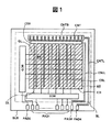
図1は本発明による表示装置の第1実施例の構成を模式的に説明するブロック図である。本実施例の表示装置は、ガラス基板SUB上に走査駆動回路GDRとデータ駆動回路DDRを有する。 FIG. 1 is a block diagram schematically illustrating the configuration of a first embodiment of the display device according to the present invention. The display device of the present embodiment has a scanning drive circuit GDR and a data drive circuit DDR on a glass substrate SUB.
そして、マトリクスに形成された走査駆動回路GDRで駆動される(走査される)走査線GL、データ駆動回路DDRで駆動されるデータ線DL、電流供給線CSLで囲まれた領域に1画素が形成される。また、基板SUBの1の辺には外部回路から走査駆動回路GDR、データ駆動回路DDRへの信号や電圧を供給するための端子パッドPAD1、PAD2が形成されている。 Then, one pixel is formed in a region surrounded by the scanning line GL driven (scanned) by the scanning driving circuit GDR formed in the matrix, the data line DL driven by the data driving circuit DDR, and the current supply line CSL. Is done. On one side of the substrate SUB, terminal pads PAD1 and PAD2 for supplying signals and voltages from the external circuit to the scan drive circuit GDR and the data drive circuit DDR are formed.
図2は図1における1画素の画素回路の構成図である。本実施例の概略構成は、1画素はデータ線DL(m+1)と走査線GL(n+1)、GL(n)および電流供給線CSLで囲まれた領域に形成される。ここでは、現在走査されている(選択されている)走査線をGL(n+1)として説明する。 FIG. 2 is a configuration diagram of a pixel circuit of one pixel in FIG. In the schematic configuration of this embodiment, one pixel is formed in a region surrounded by the data line DL (m + 1), the scanning lines GL (n + 1) and GL (n), and the current supply line CSL. Here, a description will be given assuming that the currently scanned (selected) scanning line is GL (n + 1).
走査線GL(n+1)で選択されている複数の画素のうち、画素PXに着目する。アクティブ素子である第1の薄膜トランジスタTFT1はスイッチングトランジスタ、第2の薄膜トランジスタTFT2はドライバトランジスタである。第1の薄膜トランジスタTFT1のゲートは走査線GL(n+1)に接続され、そのドレインはデータ線DL(m+1)に、ソースは第2薄膜トランジスタTFT2のゲートに接続されている。 Attention is paid to the pixel PX among the plurality of pixels selected by the scanning line GL (n + 1). The first thin film transistor TFT1, which is an active element, is a switching transistor, and the second thin film transistor TFT2 is a driver transistor. The gate of the first thin film transistor TFT1 is connected to the scanning line GL (n + 1), the drain is connected to the data line DL (m + 1), and the source is connected to the gate of the second thin film transistor TFT2.
第2の薄膜トランジスタTFT2のドレインは図1に示した電流供給線バスラインCSBから電流が供給される電流供給線CSLに接続されている。そして、そのソースはOLED24の第1の電極層ADに接続されている。第1の薄膜トランジスタTFT1のソースと第2の薄膜トランジスタTFT2のゲートの接続点にはデータ信号保持素子としてのコンデンサCPRの一方の端子が接続され、他方の端子は直前の走査線GL(n)に接続されている。 The drain of the second thin film transistor TFT2 is connected to the current supply line CSL to which a current is supplied from the current supply line bus line CSB shown in FIG. The source is connected to the first electrode layer AD of the OLED 24. One terminal of a capacitor CPR as a data signal holding element is connected to a connection point between the source of the first thin film transistor TFT1 and the gate of the second thin film transistor TFT2, and the other terminal is connected to the immediately preceding scanning line GL (n). Have been.
図2に示した1画素の回路構成において、第1の薄膜トランジスタTFT1のソースと第2の薄膜トランジスタTFT2のゲートの接続点に接続されるコンデンサCPRの一方の端子は+極であり、走査線GL(n)に接続される他方の端子は−極である。 In the circuit configuration of one pixel shown in FIG. 2, one terminal of the capacitor CPR connected to the connection point between the source of the first thin film transistor TFT1 and the gate of the second thin film transistor TFT2 is a positive electrode, and the scanning line GL ( The other terminal connected to n) is a negative pole.
また、有機発光素子OLEDは第1の電極層ADと第2の電極層CDの間に有機発光層(図示せず)を挟んだ構成であり、第1の電極層ADは第2の薄膜トランジスタTFT2のソース電極に接続し、第2の電極層CDは全画素にわたってべた形成されて図1の第2電極接続電極層CNTBに接続している。 The organic light emitting element OLED has a configuration in which an organic light emitting layer (not shown) is sandwiched between a first electrode layer AD and a second electrode layer CD, and the first electrode layer AD is formed of a second thin film transistor TFT2. The second electrode layer CD is solidly formed over all the pixels and is connected to the second electrode connection electrode layer CNTB in FIG.
この第2電極接続電極層CNTBは、所謂電流引抜き配線(電極)であり、基板の下層に前記端子パッドPAD1、PAD2と同層に形成されており、第2の電極層CDをコンタクトホールCNTで接続し、第2電極接続電極引回しラインCNTLで前記端子パッドPAD1、PAD2と同層に形成された端子PAD4に接続されている。 The second electrode connection electrode layer CNTB is a so-called current extraction wiring (electrode), is formed in the same layer as the terminal pads PAD1 and PAD2 below the substrate, and connects the second electrode layer CD with the contact hole CNT. The terminal pads PAD1 and PAD2 are connected to a terminal PAD4 formed on the same layer as the terminal pads PAD1 and PAD2 by a second electrode connection electrode lead line CNTL.
なお、第1の電極層の配線である電流供給線CSLも電流供給線バスラインCSBと電流供給線引回しラインCSLLで前記端子パッドPAD1、PAD2と同層に形成された端子PAD3に接続されている。上記第2電極接続電極層CNTBは電流供給線バスラインCSBよりも基板の外側、かつ点線で示した基板の封止領域SLの内側に配置されている。 The current supply line CSL, which is a wiring of the first electrode layer, is also connected to a terminal PAD3 formed on the same layer as the terminal pads PAD1, PAD2 by a current supply line bus line CSB and a current supply line routing line CSLL. I have. The second electrode connection electrode layer CNTB is disposed outside the substrate and inside the sealing region SL of the substrate indicated by the dotted line, relative to the current supply line bus line CSB.
このように、第2の電極層CDをコンタクトホールCNTで接続する第2電極接続電極層CNTBを電流供給線バスラインCSBよりも基板SUBの外側で、かつシール領域の内側に配置したことで、フレキシブルプリント基板を介して1辺で外部回路と接続する方式における基板上のレイアウトが容易となる。 As described above, by arranging the second electrode connection electrode layer CNTB connecting the second electrode layer CD by the contact hole CNT outside the substrate SUB and inside the seal region from the current supply line bus line CSB, The layout on the board in a system in which one side is connected to an external circuit via a flexible printed board is facilitated.
第1の薄膜トランジスタTFT1のターンオンでコンデサCPRに書き込まれ、電荷量として保持されたデータ信号は第1の薄膜トランジスタTFT1のターンオフに伴う第2の薄膜トランジスタTFT2のターンオンで電流供給線CSLからの電流を当該コンデンサCPRに保持された電荷量(データ信号の階調を示す)で制御された電流量として有機発光素子OLEに流す。 The data signal written into the capacitor CPR when the first thin film transistor TFT1 is turned on and held as an electric charge is converted from the current from the current supply line CSL when the second thin film transistor TFT2 is turned on when the first thin film transistor TFT1 is turned off. An electric current is supplied to the organic light emitting element OLE as a current amount controlled by the electric charge amount (indicating the gradation of the data signal) held in the CPR.
有機発光素子OLEDは供給される電流量にほぼ比例した輝度で、かつ当該有機発光素子を構成する有機発光層OLEの材料に依存した色で発光する。カラー表示の場合は、通常は赤、緑、青の画素毎に有機発光層材料を変えるか、あるいは白色の有機発光層材料と各色のカラーフィルタの組合せを用いる。 The organic light emitting element OLED emits light with a luminance substantially proportional to the amount of supplied current and a color depending on the material of the organic light emitting layer OLE constituting the organic light emitting element. In the case of color display, usually, the organic light emitting layer material is changed for each of red, green, and blue pixels, or a combination of a white organic light emitting layer material and a color filter of each color is used.
なお、データ信号の与え方はアナログ量でも、あるいは時分割のデジタル量でもよい。また、階調制御は、赤、緑、青の各画素の面積を分割した面積階調方式を組合せてもよい。 The data signal may be supplied in an analog amount or a time-division digital amount. Further, the gradation control may be combined with an area gradation method in which the area of each pixel of red, green and blue is divided.
本実施例では、電流供給線バスラインCSBと、各画素回路の発光動作後に第2の電極層CDから流れ出る電流を基板の下層に形成した全画素共通に形成した電流引抜き配線である第2電極接続電極層CNTBから第2電極接続電極引回しラインCNTLで端子パッドPAD4から外部回路に流出させるように構成したものである。 In the present embodiment, the current supply line bus line CSB and the second electrode, which is a current extraction wiring formed in the lower layer of the substrate and common to all pixels, is formed by applying a current flowing from the second electrode layer CD after the light emission operation of each pixel circuit. The connection electrode layer CNTB is configured to flow out from the terminal pad PAD4 to an external circuit through the second electrode connection electrode leading line CNTL.
そのため、本実施例では、上層にべた形成した全画素共通の第2の電極層CDをコンタクトホールCNTで第2電極接続電極層CNTBに接続している。第2電極接続電極引回しラインCNTLも第2電極接続電極層CNTBと同層に形成される。 Therefore, in the present embodiment, the second electrode layer CD which is formed on the upper layer and is common to all pixels is connected to the second electrode connection electrode layer CNTB through the contact hole CNT. The second electrode connection electrode routing line CNTL is also formed in the same layer as the second electrode connection electrode layer CNTB.
通常、この種の表示装置では、信頼性を確保するために缶などを用いた封止構造を採用している。基板SUBには、この封止缶詰を接着するためのシール領域が設けられている。このシール領域の内側に上記の第2電極接続電極層CNTBや第2電極接続電極引回しラインCNTLを形成している。そして、少なくとも上記の第2電極接続電極層CNTBを電流供給線バスラインCSBの外側に配置している。 Usually, this type of display device employs a sealing structure using a can or the like in order to ensure reliability. The substrate SUB is provided with a seal area for bonding the sealing can. The second electrode connection electrode layer CNTB and the second electrode connection electrode wiring line CNTL are formed inside the seal region. Then, at least the second electrode connection electrode layer CNTB is arranged outside the current supply line bus line CSB.
上記第2電極接続電極層CNTB等は基板の下層に形成され、その上に絶縁層や保護膜が積層されるので、第2電極や第2電極接続電極層、好ましくは第2電極接続電極引回しラインも含めて外気との接触がなくなり、その腐食が防止されるため、信頼性が向上し、高品質の表示を可能とした表示装置を提供することができる。なお、上記のコンタクトホールの個数は1つでもよいが、複数個設けた方がより多くの電流を安定して流すことができるため、本実施例では複数個設けている。 The second electrode connection electrode layer CNTB and the like are formed in a lower layer of the substrate, and an insulating layer and a protective film are laminated thereon, so that the second electrode and the second electrode connection electrode layer, preferably the second electrode connection electrode layer are formed. Since there is no contact with the outside air including the turning line and its corrosion is prevented, it is possible to provide a display device with improved reliability and high quality display. Although the number of the above-mentioned contact holes may be one, a plurality of the contact holes are provided in this embodiment because a larger amount of the current can be supplied stably.
図3は本発明による表示装置の発光メカニズムを説明する1画素付近の模式図、図4は第2電極層と第2電極接続電極層との接続部分を説明する模式図である。図1と同一参照符号は同一部分に対応する。また、図中の参照符号Iで示した矢印は発光に寄与する電流の経路を示す。 FIG. 3 is a schematic diagram illustrating a light emitting mechanism of a display device according to the present invention in the vicinity of one pixel, and FIG. 4 is a schematic diagram illustrating a connection portion between a second electrode layer and a second electrode connection electrode layer. The same reference numerals as those in FIG. 1 correspond to the same parts. The arrow indicated by the reference numeral I in the drawing indicates the path of a current that contributes to light emission.
薄膜トランジスタTFT2はドライバトランジスタである。この薄膜トランジスタTFT2がゲート線GLで選択されたとき、電流供給線バスラインから分岐した電流供給線より、コンデンサに保持されたデータ信号に応じた階調の電流値の電流Iが当該薄膜トランジスタTFT2を通して有機発光素子OLEDの第1の電極層ADに供給される。 The thin film transistor TFT2 is a driver transistor. When the thin film transistor TFT2 is selected by the gate line GL, a current I of a gradation value corresponding to the data signal held in the capacitor is supplied from the current supply line branched from the current supply line bus line through the thin film transistor TFT2. The light is supplied to the first electrode layer AD of the light emitting element OLED.
有機発光素子OLEDは、その有機発光層OLE内で第2の電極層CDからの電子と第1の電極層ADからのホールとが再結合し、当該有機発光層OLEの材料特性に応じたスペクトルの光Lを発光する。第1の電極層ADは各画素毎に独立であるが、第2の電極層CDは全画素についてべた膜状に形成されている。薄膜トランジスタTFT2から有機発光素子OLEDを通った電流Iは第2の電極層CDから図4に示した第2電極接続電極層CNTBを通して図1の第2電極接続電極引回しラインCNTLから端子パッドPAD4に流出する。このような画素が多数マトリクス配列されて2次元の表示装置が構成される。 In the organic light emitting element OLED, electrons from the second electrode layer CD and holes from the first electrode layer AD are recombined in the organic light emitting layer OLE, and the spectrum according to the material characteristics of the organic light emitting layer OLE is obtained. The light L is emitted. The first electrode layer AD is independent for each pixel, but the second electrode layer CD is formed in a solid film for all pixels. The current I passing from the thin film transistor TFT2 through the organic light emitting element OLED passes from the second electrode layer CD through the second electrode connection electrode layer CNTB shown in FIG. 4 to the terminal pad PAD4 from the second electrode connection electrode routing line CNTL of FIG. leak. A large number of such pixels are arranged in a matrix to form a two-dimensional display device.
図5は本発明による表示装置の第2実施例の構成を模式的に説明するブロック図である。図1と同一参照符号は同一機能部分に対応する。本実施例では、電流供給線CSLを接続する電流供給線バスラインCSBの2つの端子パッドPAD3とPAD3’、および第2電極接続電極層CNTBの端子パッドPAD4をデータ駆動回路の端子パッドPAD1および走査駆動回路GDRの端子パッドPAD2が配置される基板の1の辺と反対側の辺に設けた。 FIG. 5 is a block diagram schematically illustrating the configuration of a second embodiment of the display device according to the present invention. The same reference numerals as those in FIG. 1 correspond to the same functional parts. In this embodiment, the two terminal pads PAD3 and PAD3 'of the current supply line bus line CSB connecting the current supply line CSL and the terminal pad PAD4 of the second electrode connection electrode layer CNTB are used as the terminal pad PAD1 of the data drive circuit and the scanning. The terminal pad PAD2 of the drive circuit GDR was provided on the side opposite to the side of the substrate on which the terminal pad PAD2 was disposed.
本実施例によっても、第2の電極層CDをコンタクトホールCNTで接続する第2電極接続電極層CNTBを電流供給線バスラインCSBよりも基板SUBの外側で、かつシール領域の内側に配置したことで基板上のレイアウトが容易となる。 Also according to the present embodiment, the second electrode connection electrode layer CNTB connecting the second electrode layer CD with the contact hole CNT is disposed outside the substrate SUB and inside the seal region with respect to the current supply line bus line CSB. This facilitates layout on the substrate.
本実施例のように、電流供給線バスラインCSBからその端子パッドPAD3とPAD3’に引き回す電流供給線引回しラインCSLL、および第2電極接続電極層CNTBと端子パッドPAD4間を接続する第2電極接続電極引回しラインCNTLの基板上での引回し長さが短くなるため、より均一な電流供給と電流引抜きが可能となる。これにより、表示領域での発光分布が均一となり、より高品質の表示が得られる。なお、電流供給線引回しラインCSLLは2本としているが、何れか一方であってもよい。図5に示したように、電流供給線引回しラインCSLLを電流供給線バスラインCSBの一方及び他方からそれぞれ引き出して2本とした場合は対称性が良くなるという効果がある。 As in the present embodiment, the current supply line routing line CSLL that extends from the current supply line bus line CSB to the terminal pads PAD3 and PAD3 ′, and the second electrode that connects the second electrode connection electrode layer CNTB and the terminal pad PAD4. Since the length of the connection electrode routing line CNTL on the substrate is reduced, more uniform current supply and current extraction are possible. Thereby, the light emission distribution in the display area becomes uniform, and higher quality display can be obtained. Although the number of the current supply line routing lines CSLL is two, any one of them may be used. As shown in FIG. 5, when two current supply line routing lines CSLL are drawn out from one and the other of the current supply line bus lines CSB, respectively, there is an effect that symmetry is improved.
本実施例によって、第2の電極層CDをコンタクトホールCNTで接続する第2電極接続電極層CNTBを電流供給線バスラインCSBよりも基板SUBの外側で、かつシール領域の内側に配置したことで、フレキシブルプリント基板を介して対向する2辺で外部回路と接続する方式における基板上のレイアウトが容易となる。 According to the present embodiment, the second electrode connection electrode layer CNTB that connects the second electrode layer CD with the contact hole CNT is disposed outside the substrate SUB and inside the seal region from the current supply line bus line CSB. In addition, the layout on the board in the method of connecting to the external circuit on the two sides facing each other via the flexible printed board is facilitated.
また、本実施例の構成としたことで、シール領域の近傍における配線パターンが少なくなるため、シール材料をUV硬化させる際のUV光の遮蔽物が少なくなり、当該シール材料を効果的に硬化させることができる。これにより、確実な封止が可能となり、表示装置の信頼性をさらに向上できる。 In addition, since the wiring pattern in the vicinity of the sealing region is reduced by employing the configuration of the present embodiment, the number of shielding objects of UV light when the sealing material is cured by UV is reduced, and the sealing material is effectively cured. be able to. As a result, reliable sealing becomes possible, and the reliability of the display device can be further improved.
図6は本発明による表示装置の第3実施例の構成を模式的に説明するブロック図である。図1と同一参照符号は同一機能部分に対応する。本実施例では、電流供給線CSLを接続する電流供給線バスラインCSBのパッドPAD3と第2電極接続電極層CNTBの端子パッドPAD4をデータ駆動回路の端子パッドPAD1および走査駆動回路GDRの端子パッドPAD2が配置される基板の1の辺の両端に振り分けて設けた。 FIG. 6 is a block diagram schematically illustrating the configuration of a third embodiment of the display device according to the present invention. The same reference numerals as those in FIG. 1 correspond to the same functional parts. In this embodiment, the pad PAD3 of the current supply line bus line CSB connecting the current supply line CSL and the terminal pad PAD4 of the second electrode connection electrode layer CNTB are connected to the terminal pad PAD1 of the data drive circuit and the terminal pad PAD2 of the scan drive circuit GDR. Are arranged at both ends of one side of the substrate on which the are arranged.
前記第1〜第2実施例と同様に、第2の電極層CDをコンタクトホールCNTで接続する第2電極接続電極層CNTBを電流供給線バスラインCSBよりも基板SUBの外側で、かつシール領域の内側に配置した。他の構成は図1と同様なので繰り返しの説明は省略する。 As in the first and second embodiments, the second electrode connection electrode layer CNTB connecting the second electrode layer CD with the contact hole CNT is located outside the substrate SUB with respect to the current supply line bus line CSB and in the sealing area. Placed inside. Other configurations are the same as those in FIG.
本実施例によっても、第2の電極層CDをコンタクトホールCNTで接続する第2電極接続電極層CNTBを電流供給線バスラインCSBよりも基板SUBの外側で、かつシール領域の内側に配置したことで、フレキシブルプリント基板を介して1辺で外部回路と接続する方式における基板上のレイアウトが容易となる。 Also according to the present embodiment, the second electrode connection electrode layer CNTB connecting the second electrode layer CD with the contact hole CNT is disposed outside the substrate SUB and inside the seal region with respect to the current supply line bus line CSB. This facilitates the layout on the board in a system in which one side is connected to an external circuit via a flexible printed board.
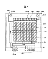
図7は本発明による表示装置の第4実施例の構成を模式的に説明するブロック図である。図1と同一参照符号は同一機能部分に対応する。本実施例では、電流供給線CSLを接続する電流供給線バスラインCSBのパッドPAD3と第2電極接続電極層CNTBの端子パッドPAD4をデータ駆動回路の端子パッドPAD1および走査駆動回路GDRの端子パッドPAD2が配置される基板の1の辺と反対側の辺に設けた。 FIG. 7 is a block diagram schematically illustrating a configuration of a fourth embodiment of the display device according to the present invention. The same reference numerals as those in FIG. 1 correspond to the same functional parts. In this embodiment, the pad PAD3 of the current supply line bus line CSB connecting the current supply line CSL and the terminal pad PAD4 of the second electrode connection electrode layer CNTB are connected to the terminal pad PAD1 of the data drive circuit and the terminal pad PAD2 of the scan drive circuit GDR. Is provided on the side opposite to the one side of the substrate on which is disposed.
前記第1〜第3実施例と同様に、第2の電極層CDをコンタクトホールCNTで接続する第2電極接続電極層CNTBを電流供給線バスラインCSBよりも基板SUBの外側で、かつシール領域の内側に配置した。 As in the first to third embodiments, the second electrode connection electrode layer CNTB connecting the second electrode layer CD with the contact hole CNT is located outside the substrate SUB with respect to the current supply line bus line CSB and the sealing area. Placed inside.
本実施例によっても、第2の電極層CDをコンタクトホールCNTで接続する第2電極接続電極層CNTBを電流供給線バスラインCSBよりも基板SUBの外側で、かつシール領域の内側に配置したことで、フレキシブルプリント基板を介して対向する2辺で外部回路と接続する方式における基板上のレイアウトが容易となる。他の構成は図6と同様なので繰り返しの説明は省略する。 Also according to the present embodiment, the second electrode connection electrode layer CNTB connecting the second electrode layer CD with the contact hole CNT is disposed outside the substrate SUB and inside the seal region with respect to the current supply line bus line CSB. This facilitates the layout on the board in a method of connecting to an external circuit on two sides facing each other via the flexible printed board. Other configurations are the same as those in FIG.
本実施例のように、電流供給線バスラインCSBからその端子パッドPAD3に引き回す電流供給線引回しラインCSLL、および第2電極接続電極層CNTBと端子パッドPAD4間を接続する第2電極接続電極引回しラインCNTLの基板上での引回し長さが短くなるため、より均一な電流供給と電流引抜きが可能となる。これにより、表示領域での発光分布が均一となり、より高品質の表示が得られる。 As in the present embodiment, the current supply line routing line CSLL that extends from the current supply line bus line CSB to the terminal pad PAD3, and the second electrode connection electrode connection that connects the second electrode connection electrode layer CNTB and the terminal pad PAD4. Since the length of the routing line CNTL on the substrate is reduced, more uniform current supply and current extraction are possible. Thereby, the light emission distribution in the display area becomes uniform, and higher quality display can be obtained.
また、本実施例の構成としたことで、シール領域の近傍における配線パターンが少なくなるため、シール材料をUV硬化させる際のUV光の遮蔽物が少なくなり、当該シール材料を効果的に硬化させることができる。これにより、確実な封止が可能となり、表示装置の信頼性をさらに向上できる。 In addition, since the wiring pattern in the vicinity of the sealing region is reduced by employing the configuration of the present embodiment, the number of shielding objects of UV light when the sealing material is cured by UV is reduced, and the sealing material is effectively cured. be able to. As a result, reliable sealing becomes possible, and the reliability of the display device can be further improved.
以上説明した第2〜第4実施例では、電流路である電流供給線引回しラインCSLLと第2電極接続電極引回しラインCNTLは、それぞれ基板上の広い領域に充分な太さの配線を形成でき、安定な電流路を確保することができる。また、特に第2実施例および第4実施例のように、パッドとの間の距離が短い場合は、より安定な電流路を確保することができる。 In the second to fourth embodiments described above, the current supply line routing line CSLL and the second electrode connection electrode routing line CNTL, which are current paths, each form a sufficiently thick wiring in a wide area on the substrate. As a result, a stable current path can be secured. In particular, when the distance between the pad and the pad is short as in the second and fourth embodiments, a more stable current path can be secured.
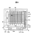
図8は本発明による表示装置の第5実施例の構成を模式的に説明するブロック図である。図1と同一参照符号は同一機能部分に対応する。本実施例では、基板上において、第2電極接続電極層CNTBを端子PAD1〜4を配置した辺に隣接して前記ゲート走査駆動回路GDRとは反対側の辺、かつ前記電流供給線引回しラインCSLLよりも外側に設けた。 FIG. 8 is a block diagram schematically illustrating the configuration of a fifth embodiment of the display device according to the present invention. The same reference numerals as those in FIG. 1 correspond to the same functional parts. In the present embodiment, on the substrate, the second electrode connection electrode layer CNTB is adjacent to the side where the terminals PAD1 to PAD4 are arranged, the side opposite to the gate scanning drive circuit GDR, and the current supply line routing line. It was provided outside CSLL.
本実施例によって、第2の電極層CDをコンタクトホールCNTで接続する第2電極接続電極層CNTBを電流供給線バスラインCSBを端子パッドPAD3に引き回す電流供給線引回しラインCSLLよりも基板SUBの外側で、かつシール領域の内側に配置したことで、ゲート走査駆動回路GDRと対称配置のレイアウトとなり、全体としてバランスの取れた配置とすることができる。他の構成は図1と同様なので繰り返しの説明は省略する。 According to this embodiment, the second electrode connection electrode layer CNTB connecting the second electrode layer CD with the contact hole CNT is connected to the current supply line bus line CSB to the terminal pad PAD3. By arranging it outside and inside the seal region, the layout becomes symmetrically arranged with the gate scanning drive circuit GDR, and the arrangement can be balanced as a whole. Other configurations are the same as those in FIG.
また、本実施例のように、端子パッドPAD4と第2電極接続電極引回しラインCNTLの基板上での引回し長さが短くなるため、より均一な電流供給と電流引抜きが可能となる。これにより、表示領域での発光分布が均一となり、より高品質の表示が得られる。 Further, as in the present embodiment, the length of the terminal pad PAD4 and the second electrode connection electrode wiring line CNTL on the substrate is shortened, so that more uniform current supply and current extraction are possible. Thereby, the light emission distribution in the display area becomes uniform, and higher quality display can be obtained.
なお、上記の各実施例は、第1の電極層と第2の電極層のそれぞれを陰極層と陽極層に対応させることができるが、本発明はこれらを入れ換えた構造に対しても同様に適用できる。また、本発明は上記したOLEDを用いた表示装置に限るものではなく、OLEDと同様の発光動作で表示を行う他の表示装置にも同様に適用できる。 In each of the above embodiments, the first electrode layer and the second electrode layer can correspond to the cathode layer and the anode layer, respectively. However, the present invention similarly applies to a structure in which these are replaced. Applicable. Further, the present invention is not limited to the display device using the above-described OLED, but can be similarly applied to other display devices that perform display by the same light emitting operation as the OLED.
SUB 基板
GL ゲート線(走査線)
DL データ線
CSL 電流供給線
CSB 電流供給線バスライン
CSLL 電流供給線引回しライン
CD 陰極
CDT コンタクトホール
CNTB 陰極接続電極層
CNTL 陰極接続電極引回しライン
AD 陽極
OLE 有機発光層
OLED 有機発光素子。
SUB substrate GL Gate line (scan line)
DL Data line CSL Current supply line CSB Current supply line bus line CSLL Current supply line lead line CD Cathode CDT Contact hole CNTB Cathode connection electrode layer CNTL Cathode connection electrode lead line AD Anode OLE Organic light emitting layer OLED Organic light emitting element.
Claims (9)
前記基板上の前記封止領域内且つ前記表示領域の外側に設けられた前記複数の走査線に走査信号を供給する走査駆動回路及び前記複数のデータ線にデータ信号を供給するデータ駆動回路、
前記画素の夫々に設けられた発光素子に電流を供給する複数の電流供給線、及び
前記基板の第1辺の前記封止領域より外側に夫々設けられた、前記走査駆動回路と電気的に接続される第1の端子パッド、前記データ駆動回路と電気的に接続される第2の端子パッド、並びに前記複数の電流供給線と電気的に接続される第3の端子パッド、を備え、
前記複数の画素の各々には、前記複数の走査線の一つに供給される前記走査信号によりターンオンされる第1のアクティブ素子と、該第1のアクティブ素子のターンオンに応じて前記データ線の一つから供給されるデータ信号を保持するデータ保持素子と、該データ保持素子に保持されたデータ信号に従って前記電流供給線からの電流を前記発光素子に供給して該発光素子を発光させる第2のアクティブ素子とを有する画素回路が設けられ、
前記複数の画素の各々に設けられた前記発光素子は、前記画素回路を覆う保護膜上に形成され且つ前記第2のアクティブ素子から前記電流を受ける第1の電極層と、該第1の電極層上に形成された有機発光層と、該有機発光層上に形成され且つ該複数の画素を覆う第2の電極層とで構成され、
前記基板の前記第1辺とは異なる第2辺に沿う前記封止領域内には、前記第2の電極層に電気的に接続される第2電極接続電極層が、該第2の電極層より下層に且つ前記保護膜で被覆されて形成され、該第2の電極層は前記保護膜に形成されたコンタクトホールを通して該第2電極接続電極層に接し、
前記第2電極接続電極層は前記基板の前記第2辺から前記第1辺へ延在する第2電極接続電極引き回しラインにより該基板の該第1辺の前記封止領域より外側に夫々設けられた第4の端子パッドに電気的に接続されていることを特徴とする表示装置。 A display region consisting of a plurality of pixels provided at each intersection of a plurality of scans arranged in a matrix in a sealing region on the substrate and a plurality of data lines intersecting the plurality of scan lines,
A scan drive circuit that supplies a scan signal to the plurality of scan lines provided in the sealing area and outside the display area on the substrate, and a data drive circuit that supplies a data signal to the plurality of data lines;
A plurality of current supply lines for supplying a current to a light emitting element provided in each of the pixels; and a plurality of current supply lines electrically connected to the scan driving circuit provided outside the sealing region on a first side of the substrate. A first terminal pad, a second terminal pad electrically connected to the data driving circuit, and a third terminal pad electrically connected to the plurality of current supply lines.
Each of the plurality of pixels has a first active element that is turned on by the scan signal supplied to one of the plurality of scan lines, and a data line that is turned on in response to turn-on of the first active element. A data holding element for holding a data signal supplied from one of them, and a second light source for supplying a current from the current supply line to the light emitting element in accordance with the data signal held in the data holding element to cause the light emitting element to emit light. A pixel circuit having an active element of
A light emitting element provided on each of the plurality of pixels, a first electrode layer formed on a protective film covering the pixel circuit and receiving the current from the second active element; An organic light emitting layer formed on the layer, and a second electrode layer formed on the organic light emitting layer and covering the plurality of pixels,
A second electrode connecting electrode layer electrically connected to the second electrode layer is provided in the sealing region along a second side different from the first side of the substrate. Forming a lower layer and being covered with the protective film, wherein the second electrode layer is in contact with the second electrode connection electrode layer through a contact hole formed in the protective film;
The second electrode connection electrode layer is provided outside the sealing region on the first side of the substrate by a second electrode connection electrode wiring line extending from the second side to the first side of the substrate. A display device electrically connected to the fourth terminal pad.
前記電流供給線バスラインは、前記基板の前記他辺から前記第1辺へ延在する電流供給線引回しラインにより第3の端子パッドに電気的に接続されていることを特徴とする請求項1に記載の表示装置。 The plurality of current supply lines are electrically connected to a current supply line bus line formed by being covered with the protective film in the sealing region on another side different from the first side of the substrate,
The current supply line bus line is electrically connected to a third terminal pad by a current supply line routing line extending from the other side of the substrate to the first side. 2. The display device according to 1.
The second electrode connection electrode routing line and the current supply line routing line are formed in the sealing region along a third side adjacent to the first side and the second side of the substrate, respectively. The display device according to claim 8, wherein a current supply line routing line is disposed between the display region and the second electrode connection electrode routing line.
Priority Applications (1)
| Application Number | Priority Date | Filing Date | Title |
|---|---|---|---|
| JP2004217260A JP2004355014A (en) | 2004-07-26 | 2004-07-26 | Display device |
Applications Claiming Priority (1)
| Application Number | Priority Date | Filing Date | Title |
|---|---|---|---|
| JP2004217260A JP2004355014A (en) | 2004-07-26 | 2004-07-26 | Display device |
Related Parent Applications (1)
| Application Number | Title | Priority Date | Filing Date |
|---|---|---|---|
| JP2001092836A Division JP3608614B2 (en) | 2001-03-28 | 2001-03-28 | Display device |
Related Child Applications (1)
| Application Number | Title | Priority Date | Filing Date |
|---|---|---|---|
| JP2007226206A Division JP5179806B2 (en) | 2007-08-31 | 2007-08-31 | Display device |
Publications (1)
| Publication Number | Publication Date |
|---|---|
| JP2004355014A true JP2004355014A (en) | 2004-12-16 |
Family
ID=34056404
Family Applications (1)
| Application Number | Title | Priority Date | Filing Date |
|---|---|---|---|
| JP2004217260A Pending JP2004355014A (en) | 2004-07-26 | 2004-07-26 | Display device |
Country Status (1)
| Country | Link |
|---|---|
| JP (1) | JP2004355014A (en) |
Cited By (4)
| Publication number | Priority date | Publication date | Assignee | Title |
|---|---|---|---|---|
| JP2009123538A (en) * | 2007-11-15 | 2009-06-04 | Sony Corp | Organic electroluminescence display |
| JP2013061663A (en) * | 2004-09-17 | 2013-04-04 | Semiconductor Energy Lab Co Ltd | Display device |
| US9117784B2 (en) | 2013-10-10 | 2015-08-25 | Seiko Epson Corporation | Light-emitting device and electronic apparatus |
| JP2022515578A (en) * | 2019-01-08 | 2022-02-21 | 京東方科技集團股▲ふん▼有限公司 | Array board and display device |
Citations (6)
| Publication number | Priority date | Publication date | Assignee | Title |
|---|---|---|---|---|
| JPS5264891A (en) * | 1975-11-21 | 1977-05-28 | Westinghouse Electric Corp | Electroluminescent display panel and method of producing same |
| JPH0431299U (en) * | 1990-07-06 | 1992-03-13 | ||
| JPH11109886A (en) * | 1997-10-03 | 1999-04-23 | Sanyo Electric Co Ltd | Display device |
| JPH11109399A (en) * | 1997-10-03 | 1999-04-23 | Sanyo Electric Co Ltd | Display device |
| JP2000173766A (en) * | 1998-09-30 | 2000-06-23 | Sanyo Electric Co Ltd | Display device |
| JP2000357584A (en) * | 1999-06-14 | 2000-12-26 | Seiko Epson Corp | Circuit board for light emitting element, electronic device and display device |
-
2004
- 2004-07-26 JP JP2004217260A patent/JP2004355014A/en active Pending
Patent Citations (7)
| Publication number | Priority date | Publication date | Assignee | Title |
|---|---|---|---|---|
| JPS5264891A (en) * | 1975-11-21 | 1977-05-28 | Westinghouse Electric Corp | Electroluminescent display panel and method of producing same |
| JPS58121081U (en) * | 1975-11-21 | 1983-08-17 | ウエスチングハウス エレクトリック コ−ポレ−ション | electroluminescent display panel |
| JPH0431299U (en) * | 1990-07-06 | 1992-03-13 | ||
| JPH11109886A (en) * | 1997-10-03 | 1999-04-23 | Sanyo Electric Co Ltd | Display device |
| JPH11109399A (en) * | 1997-10-03 | 1999-04-23 | Sanyo Electric Co Ltd | Display device |
| JP2000173766A (en) * | 1998-09-30 | 2000-06-23 | Sanyo Electric Co Ltd | Display device |
| JP2000357584A (en) * | 1999-06-14 | 2000-12-26 | Seiko Epson Corp | Circuit board for light emitting element, electronic device and display device |
Cited By (8)
| Publication number | Priority date | Publication date | Assignee | Title |
|---|---|---|---|---|
| JP2013061663A (en) * | 2004-09-17 | 2013-04-04 | Semiconductor Energy Lab Co Ltd | Display device |
| US9444069B2 (en) | 2004-09-17 | 2016-09-13 | Semiconductor Energy Laboratory Co., Ltd. | Display device and method for manufacturing the display device |
| US10096795B2 (en) | 2004-09-17 | 2018-10-09 | Semiconductor Energy Laboratory Co., Ltd. | Display device and method for manufacturing the display device |
| JP2009123538A (en) * | 2007-11-15 | 2009-06-04 | Sony Corp | Organic electroluminescence display |
| US9117784B2 (en) | 2013-10-10 | 2015-08-25 | Seiko Epson Corporation | Light-emitting device and electronic apparatus |
| JP2022515578A (en) * | 2019-01-08 | 2022-02-21 | 京東方科技集團股▲ふん▼有限公司 | Array board and display device |
| JP7562418B2 (en) | 2019-01-08 | 2024-10-07 | 京東方科技集團股▲ふん▼有限公司 | Array substrate and display device |
| US12389768B2 (en) | 2019-01-08 | 2025-08-12 | Chengdu Boe Optoelectronics Technology Co., Ltd. | Array substrate and display device |
Similar Documents
| Publication | Publication Date | Title |
|---|---|---|
| JP3608614B2 (en) | Display device | |
| JP4027614B2 (en) | Display device | |
| JP3608613B2 (en) | Display device | |
| JP5209109B2 (en) | Display device | |
| JP2004355014A (en) | Display device | |
| JP5903421B2 (en) | Display device | |
| JP5179806B2 (en) | Display device | |
| JP5442678B2 (en) | Display device | |
| JP5201712B2 (en) | Display device | |
| JP2015187735A (en) | Display device |
Legal Events
| Date | Code | Title | Description |
|---|---|---|---|
| A131 | Notification of reasons for refusal |
Free format text: JAPANESE INTERMEDIATE CODE: A131 Effective date: 20070710 |
|
| A521 | Request for written amendment filed |
Free format text: JAPANESE INTERMEDIATE CODE: A523 Effective date: 20070831 |
|
| A02 | Decision of refusal |
Free format text: JAPANESE INTERMEDIATE CODE: A02 Effective date: 20071016 |