JP2004363473A - Solid imaging device and its manufacturing method - Google Patents
Solid imaging device and its manufacturing method Download PDFInfo
- Publication number
- JP2004363473A JP2004363473A JP2003162370A JP2003162370A JP2004363473A JP 2004363473 A JP2004363473 A JP 2004363473A JP 2003162370 A JP2003162370 A JP 2003162370A JP 2003162370 A JP2003162370 A JP 2003162370A JP 2004363473 A JP2004363473 A JP 2004363473A
- Authority
- JP
- Japan
- Prior art keywords
- film
- charge transfer
- imaging device
- solid
- oxide film
- Prior art date
- Legal status (The legal status is an assumption and is not a legal conclusion. Google has not performed a legal analysis and makes no representation as to the accuracy of the status listed.)
- Pending
Links
- 238000003384 imaging method Methods 0.000 title claims abstract description 38
- 238000004519 manufacturing process Methods 0.000 title claims description 11
- 239000007787 solid Substances 0.000 title abstract 3
- 229910052581 Si3N4 Inorganic materials 0.000 claims abstract description 33
- HQVNEWCFYHHQES-UHFFFAOYSA-N silicon nitride Chemical compound N12[Si]34N5[Si]62N3[Si]51N64 HQVNEWCFYHHQES-UHFFFAOYSA-N 0.000 claims abstract description 31
- 125000006850 spacer group Chemical group 0.000 claims abstract description 25
- UFHFLCQGNIYNRP-UHFFFAOYSA-N Hydrogen Chemical compound [H][H] UFHFLCQGNIYNRP-UHFFFAOYSA-N 0.000 claims abstract description 21
- 238000006243 chemical reaction Methods 0.000 claims abstract description 21
- 239000001257 hydrogen Substances 0.000 claims abstract description 21
- 229910052739 hydrogen Inorganic materials 0.000 claims abstract description 21
- 230000002093 peripheral effect Effects 0.000 claims abstract description 9
- 229910052814 silicon oxide Inorganic materials 0.000 claims description 33
- VYPSYNLAJGMNEJ-UHFFFAOYSA-N Silicium dioxide Chemical compound O=[Si]=O VYPSYNLAJGMNEJ-UHFFFAOYSA-N 0.000 claims description 31
- 239000000758 substrate Substances 0.000 claims description 15
- XUIMIQQOPSSXEZ-UHFFFAOYSA-N Silicon Chemical compound [Si] XUIMIQQOPSSXEZ-UHFFFAOYSA-N 0.000 claims description 13
- 229910052710 silicon Inorganic materials 0.000 claims description 13
- 239000010703 silicon Substances 0.000 claims description 13
- 238000005530 etching Methods 0.000 claims description 11
- 239000010410 layer Substances 0.000 claims description 10
- 238000000034 method Methods 0.000 claims description 8
- 239000002356 single layer Substances 0.000 claims description 6
- 239000004065 semiconductor Substances 0.000 claims description 4
- 238000000059 patterning Methods 0.000 claims description 3
- 230000001590 oxidative effect Effects 0.000 claims description 2
- 230000005540 biological transmission Effects 0.000 abstract 4
- 230000002265 prevention Effects 0.000 abstract 2
- 239000010408 film Substances 0.000 description 145
- 238000000137 annealing Methods 0.000 description 7
- 229910021420 polycrystalline silicon Inorganic materials 0.000 description 6
- 238000010586 diagram Methods 0.000 description 5
- 230000000694 effects Effects 0.000 description 4
- 238000004518 low pressure chemical vapour deposition Methods 0.000 description 4
- 238000000206 photolithography Methods 0.000 description 4
- 239000007789 gas Substances 0.000 description 3
- 230000035945 sensitivity Effects 0.000 description 3
- NBIIXXVUZAFLBC-UHFFFAOYSA-N Phosphoric acid Chemical compound OP(O)(O)=O NBIIXXVUZAFLBC-UHFFFAOYSA-N 0.000 description 2
- 230000015572 biosynthetic process Effects 0.000 description 2
- 239000005380 borophosphosilicate glass Substances 0.000 description 2
- 238000005468 ion implantation Methods 0.000 description 2
- 229910052751 metal Inorganic materials 0.000 description 2
- 239000002184 metal Substances 0.000 description 2
- 230000003647 oxidation Effects 0.000 description 2
- 238000007254 oxidation reaction Methods 0.000 description 2
- 238000001020 plasma etching Methods 0.000 description 2
- ZOXJGFHDIHLPTG-UHFFFAOYSA-N Boron Chemical compound [B] ZOXJGFHDIHLPTG-UHFFFAOYSA-N 0.000 description 1
- GWEVSGVZZGPLCZ-UHFFFAOYSA-N Titan oxide Chemical compound O=[Ti]=O GWEVSGVZZGPLCZ-UHFFFAOYSA-N 0.000 description 1
- 238000010306 acid treatment Methods 0.000 description 1
- 229910000147 aluminium phosphate Inorganic materials 0.000 description 1
- 229910021417 amorphous silicon Inorganic materials 0.000 description 1
- 238000004380 ashing Methods 0.000 description 1
- 229910052796 boron Inorganic materials 0.000 description 1
- 238000010438 heat treatment Methods 0.000 description 1
- 239000011229 interlayer Substances 0.000 description 1
- 239000012528 membrane Substances 0.000 description 1
- 229910021424 microcrystalline silicon Inorganic materials 0.000 description 1
- 230000003287 optical effect Effects 0.000 description 1
- RLOWWWKZYUNIDI-UHFFFAOYSA-N phosphinic chloride Chemical compound ClP=O RLOWWWKZYUNIDI-UHFFFAOYSA-N 0.000 description 1
- 239000011347 resin Substances 0.000 description 1
- 229920005989 resin Polymers 0.000 description 1
- 238000000926 separation method Methods 0.000 description 1
- 238000005245 sintering Methods 0.000 description 1
- 239000010409 thin film Substances 0.000 description 1
- OGIDPMRJRNCKJF-UHFFFAOYSA-N titanium oxide Inorganic materials [Ti]=O OGIDPMRJRNCKJF-UHFFFAOYSA-N 0.000 description 1
- WFKWXMTUELFFGS-UHFFFAOYSA-N tungsten Chemical compound [W] WFKWXMTUELFFGS-UHFFFAOYSA-N 0.000 description 1
- 229910052721 tungsten Inorganic materials 0.000 description 1
- 239000010937 tungsten Substances 0.000 description 1
Images



Landscapes
- Solid State Image Pick-Up Elements (AREA)
- Transforming Light Signals Into Electric Signals (AREA)
Abstract
Description
【0001】
【発明の属する技術分野】
本発明は、固体撮像素子およびその製造方法に関する。
【0002】
【従来の技術】
エリアセンサ等に用いられるCCD(電荷結合素子)を用いた固体撮像素子は、フォトダイオードなどの光電変換部と、この光電変換部からの信号電荷を転送するための電荷転送電極を備えた電荷転送部とを有する。電荷転送電極は、半導体基板に形成された電荷転送路上に複数個配置され、順次駆動される。
【0003】
近年、固体撮像素子においては、撮像画素数の増加により、画素の微細化が進んでいる。それに伴い光電変換部の微細化も進み高感度を維持することが、困難になっている。
【0004】
このような状況の中で図7に示すように、画素部に反射防止膜となる窒化シリコン膜等の、酸化シリコン膜よりも屈折率の高い膜を形成した固体撮像素素子が提案されている。
【0005】
そして、画素部に水素を供給することにより、基板界面電位の低減をはかることができ、暗電流や白キズの発生を抑制することができる。これは水素アニール効果として知られている。
【0006】
ところで、図7に断面図を示すように、電荷転送電極3の表面を酸化して酸化シリコン膜6aで被覆するとともにスペーサ膜としての窒化シリコン膜6bを形成し、さらに反射防止膜となる窒化シリコン膜62を形成し、この上層に金属遮光膜71を形成した構造が提案されている(参考文献1)。
【0007】
しかしながらこの構造では、周辺回路部のアンプのトランジスタについてはノイズを低減するためにゲート酸化膜を酸化シリコン膜単層としている。これはアンプノイズ低減(熱雑音&1/f雑音成分)のためである。つまり熱雑音を低減するにはドライバーの相互コンダクタンス(gm)を大きくする必要があるがこのgmはCox増大(Gate酸化膜薄膜化)で大きく出来る。1/f雑音成分はCoxに反比例(Cox=εox/toxよりtoxには比例)するためにGate薄膜化が有効となる。
【0008】
このため、ゲート酸化膜は一括してパターニングするのではなく、窒化シリコン膜を残してパターニングする。すなわちゲート電極のパターニング工程において酸化シリコン単層であるアンプ部のゲート酸化膜がダメージを受けないように他の領域の窒化シリコン膜は残しておくようにし、窒化シリコン膜をエッチングストッパとしてゲート電極であるシリコン系導電性膜のパターニングを行う。
そして電極表面を酸化し酸化シリコン膜を形成し、この後光電変換部(画素部)の窒化シリコン膜をエッチング除去している。
【0009】
【特許文献1】
特開2002−324899号公報
【0010】
【発明が解決しようとする課題】
この状態では、ゲート酸化膜側壁、特に窒化シリコン膜2bの側壁が露呈しており、反射防止膜62としての窒化シリコンを形成すると、このゲート酸化膜の窒化シリコン膜と反射防止膜の窒化シリコン膜とがこのゲート酸化膜側壁で繋がってしまい、水素の供給路が絶たれてしまうという問題がある。
これは、暗時の白キズの原因となる。ここで白キズとは入射光のレベルにかかわらず、信号電荷が発生してしまうことをいい、画面には白いキズ状にみえる。
【0011】
本発明は前記実情に鑑みてなされたもので、白キズの発生を抑制し、信頼性の高い固体撮像素子を提供することを目的とする。
【0012】
【課題を解決するための手段】
そこで本発明は、光電変換部と、前記光電変換部で生起せしめられた電荷を転送する電荷転送電極を備えた電荷転送部と、前記電荷転送部に接続された周辺回路部とを具備し、前記光電変換部の表面を窒化シリコン膜からなる反射防止膜で被覆した固体撮像素子であって、前記電荷転送電極下のゲート酸化膜の側壁と、前記反射防止膜との間に水素透過性のスペーサ膜を介在させたことを特徴とする。
【0013】
かかる構成によれば、ゲート酸化膜の側壁と反射防止膜との間に水素透過性のスペーサ膜が介在しているため、ゲート酸化膜の窒化シリコン膜の側壁と反射防止膜との間にはスペーサ膜が介在することになり、水素アニール効果も良好に奏功し得ることになる。
ここでこのスペーサ膜は、酸化シリコン膜であるのが望ましい。これにより通常のプロセスで効率よく形成することが可能となる。
【0014】
また、このスペーサ膜は、膜厚10nm以下であるのが望ましい。さらに望ましくは5nm以下とする。これにより感度の低下を抑制するとともに、遮光膜の張り出し部分から反射して入ってくるスミアの原因となる光も抑制し、信頼性の高い固体撮像素子を形成することが可能となる。
【0015】
又上記固体撮像素子において、前記周辺回路部はゲート酸化膜が単層構造のトランジスタを含む。この場合、特に窒化シリコン膜の側壁が露呈しやすいが、スペーサの介在により、水素の透過が可能となり、白キズの発生が抑制される。
【0016】
また本発明は、光電変換部と、前記光電変換部で生起せしめられた電荷を転送する電荷転送電極を備えた電荷転送部と、前記電荷転送部に接続された周辺回路部とを具備し、前記光電変換部の表面を窒化シリコン膜からなる反射防止膜で被覆した固体撮像素子の製造方法であって、半導体基板表面に、酸化シリコン膜−窒化シリコン膜−酸化シリコン膜の3層構造膜(ONO膜)からなるゲート酸化膜を形成する工程と、前記ゲート酸化膜上にシリコン系導電性膜を形成する工程と、窒化シリコン膜をエッチングストッパとして前記シリコン系導電性膜をパターニングし電荷転送電極を形成する工程と、前記電荷転送電極表面を酸化する工程と、前記光電変換部の少なくとも画素部の前記窒化シリコン膜をエッチング除去する工程と、前記電荷転送電極下の窒化シリコンの側壁を覆うように水素透過性のスペーサを形成する工程と、反射防止膜を形成する工程とを含むことを特徴とする。
【0017】
又望ましくは、前記スペーサ膜の形成に先立ち、前記基板表面をエッチングし、酸化シリコン膜を形成する工程を含むことを特徴とする。
【0018】
【発明の実施の形態】
以下本発明の実施の形態について図面を参照しつ説明する。
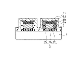
図1は、本発明の実施の形態の固体撮像素子の要部断面を示す説明図、図2および図3は、本発明の実施の形態の固体撮像素子を示す平面図およびそのA−A断面図である。また、図4乃至図6は同製造工程図である。
【0019】
この固体撮像素子は、図1および3に示すように、光電変換部30と、前記光電変換部で生起せしめられた電荷を転送する単層構造の電荷転送電極を備えた電荷転送部40とを具備した固体撮像素子であって、前記電荷転送電極下のゲート酸化膜の側壁と、前記反射防止膜との間に水素透過性のスペーサ膜を介在させたことを特徴とする。
【0020】
この構成は、感度の低下や光学特性の低下を回避しつつ、ゲート酸化膜の側壁と反射防止膜との間に水素透過性のスペーサ膜である酸化シリコン膜膜6bを介在させているため、ゲート酸化膜の窒化シリコン2bの側壁と反射防止膜との間にはスペーサ膜が介在することになり、水素アニール効果も良好に奏功し得ることになる。
【0021】
なおここで、半導体基板1としては低効率5.0〜9.5Ωcmのn型シリコン基板を用い、ゲート酸化膜2は、酸化シリコン膜2aと窒化シリコン膜2bと酸化シリコン膜2cとの3層構造膜で構成される。
【0022】
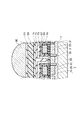
なお、図2に平面図、図3に全体断面概要図を示すように、シリコン基板1には、複数のフォトダイオード30が形成され、フォトダイオードで検出した信号電荷を転送するための電荷転送部40が、フォトダイオード30の間に形成される。
【0023】
電荷転送電極によって転送される信号電荷が移動する電荷転送チャネル31は、図1では図示していないが、電荷転送部40が延在する方向と交差する方向に形成される。
【0024】
なお、図2においては、電極間絶縁膜3の内、フォトダイオード領域と電荷転送部40との境界近傍に形成されるものの記載を省略してある。
【0025】
図3に示すように、シリコン基板1内には、フォトダイオード30、電荷転送チャネル31、チャネルストップ領域32、電荷読み出し領域33が形成され、シリコン基板1表面には、ゲート酸化膜2が形成される。ゲート酸化膜2表面には、酸化シリコン膜からなる電極間絶縁膜6aと電荷転送電極(電極3)が形成される。
【0026】
電荷転送部40は、上述したとおりであるが、図3に示すように、電荷転送部40の電荷転送電極上面には層間絶縁膜70が形成される。71は遮光膜、72はP−TEOSからなる絶縁膜、74はBPSG膜からなる平坦化層である。
【0027】
固体撮像素子の上方には、フォトダイオード30部分を除いて遮光膜71が設けられ、さらにカラーフィルタ50、マイクロレンズ60が設けられる。また、カラーフィルタ50とマイクロレンズ60との間は、絶縁性の透明樹脂等からなる平坦化層61が充填される。電荷転送部40および電極間絶縁膜6を除いて通例のものと同様であるので説明を省略する。また、図2では、いわゆるハニカム構造の固体撮像素子を示しているが、正方格子型の固体撮像素子にも適用可能であることはいうまでもない。
【0028】
次にこの固体撮像素子の製造工程について詳細に説明する。
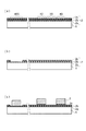
まず、図4(a)に示すように、n型のシリコン基板1表面に、膜厚35nmの酸化シリコン膜2aと、膜厚50nmの窒化シリコン膜2bと、膜厚5nmの酸化シリコン膜2cを形成し、3層構造のゲート酸化膜2を形成する。
【0029】
続いて、図4(b)に示すように、周辺回路部40Sにおいてアンプ部のトランジスタ領域に相当する部分の酸化シリコン膜2cおよび窒化シリコン膜2bを選択的に除去し、単層とする。
【0030】
この後、ゲート酸化膜2上に、SiH4を反応性ガスとして用いた減圧CVD法により、膜厚0.4μmの多結晶シリコン膜を形成する。このときの基板温度は600〜700℃とする。この後POCl3とN2とO2との混合ガス雰囲気中で900℃の熱処理を行い多結晶シリコン膜3をドーピングする(リン酸処理)。
続いて、フォトリソグラフィにより形成したレジストパターンをマスクとして、HBrとO2との混合ガス(HBr/O2:60/2(ml/min))を用いた反応性イオンエッチングにより、ゲート酸化膜2の窒化シリコン膜2bをエッチングストッパとして多結晶シリコン膜3を選択的にエッチング除去し、電極を形成する。ここでは高密度プラズマエッチング装置を用いるのが望ましい。
【0031】
続いて、必要に応じてこのレジストパターンをマスクとして、転送効率を補うためのイオン注入を行う。ここではボロンを20〜100KeV、1×10¹⁰〜1×10¹³/cm2でイオン注入する。
そして、アッシングによりレジストパターンを除去する(図4(c))。
【0032】
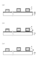
こののち、熱酸化法により、電極のパターンの表面に膜厚80nmの酸化シリコン膜からなる電極間絶縁膜6を形成する(図5(a))。
【0033】
次に酸化シリコン膜と窒化シリコン膜との高選択比のエッチングにより、画素部の窒化シリコンをエッチング除去する(図5(b))。
【0034】
次に、図5(c)に示すように、画素部の酸化シリコン膜を清浄化し、きれいな酸化シリコン膜を露出するために、軽く酸化シリコン膜をエッチングする。
【0035】
この後、全面に減圧CVD法により、図6(a)に示すように、膜厚5nmのスペーサとしての酸化シリコン膜6bを形成する。そしてフォトリソグラフィを用いて形成したマスクを介してイオン注入を行い光電変換部のpn接合(図示せず)を形成する。
【0036】
そして減圧CVD法により、図6(b)に示すように、膜厚30nmの窒化シリコン膜からなる反射防止膜62を堆積し、フォトリソグラフィにより画素部を覆うように反射防止膜を形成する。(なお電極上など不要部分では、水素透過のために開口を形成している。)
【0037】
そして図6(c)に示すように、タングステン薄膜などからなる遮光膜17を形成し、フォトリソグラフィにより光電変換部に窓を形成する。
【0038】
なお、この方法では、スペーサとしての酸化シリコン膜を反射防止膜62とONO膜構造のゲート酸化膜の側壁との間に介在させることにより、水素アニールに際してもこのスペーサによって水素の透過経路が形成され、白キズの発生を抑制することができる。
このスペーサとしての酸化シリコン膜は減圧CVD法によって形成しているため、被覆性が良好で、薄くても十分にスペーサとしての役割を果たすことができる。
【0039】
そしてこの上層に遮光膜71、膜厚100nmのP−TEOS膜72を形成した後、膜厚700nmのBPSG膜73を形成し、850℃でリフローし平坦化する。このようにして絶縁膜70を得る。
【0040】
この後、水素アニール工程を含むシンタリングを行い、基板の安定化をはかる。このときの水素アニール工程の条件は下記の通りである。
温度 380℃
時間 30分
ガス H2+N2
この後、カラーフィルタ50、平坦化層61、マイクロレンズ60などを形成して、図3に示したような固体撮像素子を得る。
【0041】
かかる構成によれば、白キズを抑制し、高感度で信頼性の高い固体撮像素子を提供することが可能となる。
【0042】
なお、上記固体撮像素子において、前記電極間分離領域としての電極間領域Gは、幅0.2μm以下であるのがのぞましい。
【0043】
なお、前記実施の形態ではゲート酸化膜はONO膜構造の3層膜で構成したがNO膜すなわち酸化シリコン膜と窒化シリコン膜との2層膜の場合にも適用可能であることはいうまでもない。
【0044】
また、前記実施の形態では、スペーサ膜として酸化シリコン膜を用いたが酸化シリコン膜に限定されることなく、陽極酸化などにより多孔化した酸化チタンなどの水素透過性膜であればよい。
【0045】
また、前記実施の形態では単層電極構造の固体撮像素子について説明したが、多層電極構造の固体撮像素子にも適用可能であることはいうまでもない。
【0046】
また前記実施の形態では、電極を形成するシリコン系導電性膜として、多結晶シリコン膜を用いたが、多結晶シリコン膜に限定されることなく、アモルファスシリコン、マイクロクリスタルシリコンなど他のシリコン系導電性膜を用いてもよい。
【0047】
また、前記電極上に金属膜を形成することにより、電極の低抵抗化をはかることができ、高速駆動が可能となる。
【0048】
【発明の効果】
以上説明してきたように、本発明の固体撮像素子によれば、反射防止膜としての窒化シリコンの形成に先立ち、酸化シリコン膜などの水素透過性膜を形成しているため、水素アニール工程が良好に行われ、白キズの発生のない信頼性の高い固体撮像素子を提供することが可能となる。
【図面の簡単な説明】
【図1】本発明の実施の形態の固体撮像素子の要部断面説明図である。
【図2】本発明の実施の形態の固体撮像素子の平面図である。
【図3】本発明の実施の形態の固体撮像素子の断面図である。
【図4】本発明の実施の形態の固体撮像素子の製造工程を示す図である。
【図5】本発明の実施の形態の固体撮像素子の製造工程を示す図である。
【図6】本発明の実施の形態の固体撮像素子の製造工程を示す図である。
【図7】従来例の固体撮像素子を示す断面図である。
【符号の説明】
1 シリコン基板
2 ゲート酸化膜
3 電荷転送電極(多結晶シリコン膜)
6a 電極間絶縁膜
6b スペーサ膜(酸化シリコン膜)
62 反射防止膜
71 遮光膜
30 フォトダイオード部
40 電荷転送部
50 カラーフィルタ
60 マイクロレンズ
70 絶縁膜[0001]
BACKGROUND OF THE INVENTION
The present invention relates to a solid-state imaging device and a manufacturing method thereof.
[0002]
[Prior art]
A solid-state imaging device using a CCD (charge coupled device) used for an area sensor or the like is a charge transfer device including a photoelectric conversion unit such as a photodiode and a charge transfer electrode for transferring a signal charge from the photoelectric conversion unit. Part. A plurality of charge transfer electrodes are arranged on the charge transfer path formed on the semiconductor substrate and are sequentially driven.
[0003]
In recent years, in a solid-state imaging device, pixel miniaturization has progressed due to an increase in the number of imaging pixels. Along with this, miniaturization of the photoelectric conversion part has progressed and it has become difficult to maintain high sensitivity.
[0004]
Under such circumstances, as shown in FIG. 7, a solid-state imaging element in which a film having a refractive index higher than that of a silicon oxide film such as a silicon nitride film serving as an antireflection film is formed in a pixel portion has been proposed. .
[0005]
Then, by supplying hydrogen to the pixel portion, the substrate interface potential can be reduced, and generation of dark current and white scratches can be suppressed. This is known as the hydrogen annealing effect.
[0006]
By the way, as shown in a cross-sectional view in FIG. 7, the surface of the
[0007]
However, in this structure, the gate oxide film is a single silicon oxide film layer in order to reduce noise in the amplifier transistors in the peripheral circuit section. This is for amplifier noise reduction (thermal noise & 1 / f noise component). That is, to reduce the thermal noise, it is necessary to increase the mutual conductance (gm) of the driver, but this gm can be increased by increasing Cox (thinning the gate oxide film). Since the 1 / f noise component is inversely proportional to Cox (Cox = εox / tox is more proportional to tox), gate thinning is effective.
[0008]
For this reason, the gate oxide film is not patterned all at once, but is patterned leaving the silicon nitride film. That is, in the patterning process of the gate electrode, the silicon oxide film in the other region is left so that the gate oxide film of the amplifier part which is a silicon oxide single layer is not damaged, and the silicon nitride film is used as an etching stopper in the gate electrode. A certain silicon type conductive film is patterned.
Then, the electrode surface is oxidized to form a silicon oxide film, and then the silicon nitride film in the photoelectric conversion portion (pixel portion) is removed by etching.
[0009]
[Patent Document 1]
Japanese Patent Laid-Open No. 2002-324899
[Problems to be solved by the invention]
In this state, the side wall of the gate oxide film, particularly the side wall of the
This causes white scratches in the dark. Here, the white scratch means that a signal charge is generated regardless of the level of incident light, and the screen looks like a white scratch.
[0011]
The present invention has been made in view of the above circumstances, and an object of the present invention is to provide a solid-state imaging device that suppresses the occurrence of white scratches and has high reliability.
[0012]
[Means for Solving the Problems]
Therefore, the present invention includes a photoelectric conversion unit, a charge transfer unit including a charge transfer electrode that transfers charges generated in the photoelectric conversion unit, and a peripheral circuit unit connected to the charge transfer unit, A solid-state imaging device in which a surface of the photoelectric conversion unit is covered with an antireflection film made of a silicon nitride film, and a hydrogen permeable film is interposed between the side wall of the gate oxide film under the charge transfer electrode and the antireflection film. A spacer film is interposed.
[0013]
According to this configuration, since the hydrogen permeable spacer film is interposed between the side wall of the gate oxide film and the antireflection film, the side wall of the silicon nitride film of the gate oxide film and the antireflection film are interposed. The spacer film is interposed, and the hydrogen annealing effect can be successfully achieved.
Here, the spacer film is preferably a silicon oxide film. Thereby, it can be formed efficiently by a normal process.
[0014]
The spacer film is desirably 10 nm or less in thickness. More preferably, it is 5 nm or less. As a result, it is possible to suppress a decrease in sensitivity and to suppress light that causes a smear reflected from the projecting portion of the light shielding film, thereby forming a highly reliable solid-state imaging device.
[0015]
In the solid-state imaging device, the peripheral circuit portion includes a transistor having a single-layer gate oxide film. In this case, the side walls of the silicon nitride film are particularly easily exposed, but the hydrogen can be transmitted through the spacers, and the occurrence of white scratches is suppressed.
[0016]
Further, the present invention comprises a photoelectric conversion unit, a charge transfer unit including a charge transfer electrode for transferring charges generated in the photoelectric conversion unit, and a peripheral circuit unit connected to the charge transfer unit, A method of manufacturing a solid-state imaging device in which a surface of the photoelectric conversion portion is covered with an antireflection film made of a silicon nitride film, and a three-layer structure film of silicon oxide film-silicon nitride film-silicon oxide film (on a semiconductor substrate surface) A step of forming a gate oxide film made of an ONO film), a step of forming a silicon-based conductive film on the gate oxide film, and patterning the silicon-based conductive film using a silicon nitride film as an etching stopper to form a charge transfer electrode A step of oxidizing the surface of the charge transfer electrode, a step of etching away the silicon nitride film of at least the pixel portion of the photoelectric conversion portion, Forming a hydrogen-permeable spacer so as to cover the sidewall of the silicon nitride under the transfer electrodes, characterized in that it comprises a step of forming an anti-reflection film.
[0017]
Preferably, the method includes a step of etching the surface of the substrate to form a silicon oxide film prior to the formation of the spacer film.
[0018]
DETAILED DESCRIPTION OF THE INVENTION
Embodiments of the present invention will be described below with reference to the drawings.
FIG. 1 is an explanatory view showing a cross section of a main part of a solid-state image sensor according to an embodiment of the present invention, and FIGS. 2 and 3 are plan views showing the solid-state image sensor according to the embodiment of the present invention and its AA cross section. FIG. 4 to 6 are manufacturing process diagrams.
[0019]
As shown in FIGS. 1 and 3, the solid-state imaging device includes a
[0020]
In this configuration, the
[0021]
Here, an n-type silicon substrate having a low efficiency of 5.0 to 9.5 Ωcm is used as the
[0022]
As shown in a plan view in FIG. 2 and an overall cross-sectional schematic diagram in FIG. 3, a plurality of
[0023]
Although not shown in FIG. 1, the
[0024]
In FIG. 2, the description of the interelectrode
[0025]
As shown in FIG. 3, a
[0026]
Although the
[0027]
Above the solid-state imaging device, a
[0028]
Next, the manufacturing process of this solid-state image sensor will be described in detail.
First, as shown in FIG. 4A, a
[0029]
Subsequently, as shown in FIG. 4B, the
[0030]
Thereafter, a polycrystalline silicon film having a thickness of 0.4 μm is formed on the
Subsequently, the
[0031]
Subsequently, ion implantation for compensating transfer efficiency is performed using this resist pattern as a mask as necessary. Here, boron is ion-implanted at 20 to 100 KeV and 1 × 10 10 to 1 × 10 13 / cm 2 .
Then, the resist pattern is removed by ashing (FIG. 4C).
[0032]
Thereafter, an interelectrode
[0033]
Next, the silicon nitride in the pixel portion is removed by etching with a high selectivity between the silicon oxide film and the silicon nitride film (FIG. 5B).
[0034]
Next, as shown in FIG. 5C, the silicon oxide film is lightly etched in order to clean the silicon oxide film in the pixel portion and expose a clean silicon oxide film.
[0035]
Thereafter, as shown in FIG. 6A, a
[0036]
Then, as shown in FIG. 6B, an
[0037]
Then, as shown in FIG. 6C, a light shielding film 17 made of a tungsten thin film or the like is formed, and a window is formed in the photoelectric conversion portion by photolithography.
[0038]
In this method, since a silicon oxide film as a spacer is interposed between the
Since the silicon oxide film as the spacer is formed by the low pressure CVD method, the coverage is good, and even if it is thin, it can sufficiently serve as the spacer.
[0039]
Then, after forming a
[0040]
Thereafter, sintering including a hydrogen annealing step is performed to stabilize the substrate. The conditions for the hydrogen annealing step at this time are as follows.
Temperature 380 ° C
Thereafter, the color filter 50, the
[0041]
According to such a configuration, it is possible to provide a solid-state imaging device that suppresses white scratches and is highly sensitive and highly reliable.
[0042]
In the solid-state imaging device, it is preferable that the inter-electrode region G as the inter-electrode separation region has a width of 0.2 μm or less.
[0043]
In the above-described embodiment, the gate oxide film is composed of a three-layer film having an ONO film structure. Absent.
[0044]
Moreover, in the said embodiment, although the silicon oxide film was used as a spacer film, it is not limited to a silicon oxide film, What is necessary is just a hydrogen permeable film | membrane, such as a titanium oxide porous by anodic oxidation.
[0045]
In the above-described embodiment, the solid-state imaging device having a single-layer electrode structure has been described. However, it is needless to say that the present invention can be applied to a solid-state imaging device having a multilayer electrode structure.
[0046]
In the above embodiment, a polycrystalline silicon film is used as the silicon-based conductive film for forming the electrode. However, the present invention is not limited to the polycrystalline silicon film, and other silicon-based conductive films such as amorphous silicon and microcrystalline silicon are used. A conductive film may be used.
[0047]
In addition, by forming a metal film on the electrode, the resistance of the electrode can be reduced, and high-speed driving is possible.
[0048]
【The invention's effect】
As described above, according to the solid-state imaging device of the present invention, a hydrogen permeable film such as a silicon oxide film is formed prior to the formation of silicon nitride as an antireflection film, so that the hydrogen annealing process is good. Thus, it is possible to provide a highly reliable solid-state imaging device free from white scratches.
[Brief description of the drawings]
FIG. 1 is an explanatory cross-sectional view of a main part of a solid-state imaging device according to an embodiment of the present invention.
FIG. 2 is a plan view of the solid-state imaging device according to the embodiment of the present invention.
FIG. 3 is a cross-sectional view of a solid-state image sensor according to an embodiment of the present invention.
FIG. 4 is a diagram showing a manufacturing process of the solid-state imaging device according to the embodiment of the present invention.
FIG. 5 is a diagram showing a manufacturing process of the solid-state imaging device according to the embodiment of the present invention.
FIG. 6 is a diagram showing a manufacturing process of the solid-state imaging device according to the embodiment of the present invention.
FIG. 7 is a cross-sectional view showing a conventional solid-state imaging device.
[Explanation of symbols]
1
6a
62
Claims (6)
前記電荷転送電極下のゲート酸化膜の側壁と、前記反射防止膜との間に水素透過性のスペーサ膜を介在させたことを特徴とする固体撮像素子。A photoelectric transfer unit, a charge transfer unit including a charge transfer electrode that transfers charges generated in the photoelectric conversion unit, and a peripheral circuit unit connected to the charge transfer unit, A solid-state imaging device having a surface coated with an antireflection film made of a silicon nitride film,
A solid-state imaging device, wherein a hydrogen permeable spacer film is interposed between a side wall of a gate oxide film under the charge transfer electrode and the antireflection film.
半導体基板表面に、酸化シリコン膜−窒化シリコン膜−酸化シリコン膜の3層構造膜(ONO膜)からなるゲート酸化膜を形成する工程と、
前記ゲート酸化膜上にシリコン系導電性膜を形成する工程と、
窒化シリコン膜をエッチングストッパとして前記シリコン系導電性膜をパターニングし電荷転送電極を形成する工程と、
前記電荷転送電極表面を酸化する工程と、
前記光電変換部の少なくとも画素部の前記窒化シリコン膜をエッチング除去する工程と、
前記電荷転送電極下の窒化シリコンの側壁を覆うように水素透過性のスペーサを形成する工程と、
反射防止膜を形成する工程と、
を含むことを特徴とする固体撮像素子の製造方法。A photoelectric transfer unit, a charge transfer unit including a charge transfer electrode that transfers charges generated in the photoelectric conversion unit, and a peripheral circuit unit connected to the charge transfer unit, A method for manufacturing a solid-state imaging device having a surface coated with an antireflection film made of a silicon nitride film,
Forming a gate oxide film composed of a three-layer structure film (ONO film) of silicon oxide film-silicon nitride film-silicon oxide film on a semiconductor substrate surface;
Forming a silicon-based conductive film on the gate oxide film;
Patterning the silicon-based conductive film using a silicon nitride film as an etching stopper to form a charge transfer electrode; and
Oxidizing the charge transfer electrode surface;
Etching the silicon nitride film of at least the pixel portion of the photoelectric conversion portion; and
Forming a hydrogen permeable spacer so as to cover a side wall of silicon nitride under the charge transfer electrode;
Forming an antireflection film;
The manufacturing method of the solid-state image sensor characterized by including.
Priority Applications (1)
| Application Number | Priority Date | Filing Date | Title |
|---|---|---|---|
| JP2003162370A JP2004363473A (en) | 2003-06-06 | 2003-06-06 | Solid imaging device and its manufacturing method |
Applications Claiming Priority (1)
| Application Number | Priority Date | Filing Date | Title |
|---|---|---|---|
| JP2003162370A JP2004363473A (en) | 2003-06-06 | 2003-06-06 | Solid imaging device and its manufacturing method |
Publications (1)
| Publication Number | Publication Date |
|---|---|
| JP2004363473A true JP2004363473A (en) | 2004-12-24 |
Family
ID=34054540
Family Applications (1)
| Application Number | Title | Priority Date | Filing Date |
|---|---|---|---|
| JP2003162370A Pending JP2004363473A (en) | 2003-06-06 | 2003-06-06 | Solid imaging device and its manufacturing method |
Country Status (1)
| Country | Link |
|---|---|
| JP (1) | JP2004363473A (en) |
Cited By (3)
| Publication number | Priority date | Publication date | Assignee | Title |
|---|---|---|---|---|
| JP2006294654A (en) * | 2005-04-05 | 2006-10-26 | Matsushita Electric Ind Co Ltd | Solid-state imaging device and manufacturing method thereof |
| JP2006324339A (en) * | 2005-05-17 | 2006-11-30 | Sony Corp | Photoelectric conversion element |
| JP2016039192A (en) * | 2014-08-06 | 2016-03-22 | ルネサスエレクトロニクス株式会社 | Manufacturing method of semiconductor integrated circuit device |
-
2003
- 2003-06-06 JP JP2003162370A patent/JP2004363473A/en active Pending
Cited By (3)
| Publication number | Priority date | Publication date | Assignee | Title |
|---|---|---|---|---|
| JP2006294654A (en) * | 2005-04-05 | 2006-10-26 | Matsushita Electric Ind Co Ltd | Solid-state imaging device and manufacturing method thereof |
| JP2006324339A (en) * | 2005-05-17 | 2006-11-30 | Sony Corp | Photoelectric conversion element |
| JP2016039192A (en) * | 2014-08-06 | 2016-03-22 | ルネサスエレクトロニクス株式会社 | Manufacturing method of semiconductor integrated circuit device |
Similar Documents
| Publication | Publication Date | Title |
|---|---|---|
| US6974715B2 (en) | Method for manufacturing CMOS image sensor using spacer etching barrier film | |
| JP2012182426A (en) | Solid state image pickup device, image pickup system using solid state image pickup device and solis state image pickup device manufacturing method | |
| CN102637712B (en) | Semiconductor device and method for manufacturing the same | |
| WO2017028546A1 (en) | Backside image sensor with three-dimensional transistor structure and formation method therefor | |
| JP4473240B2 (en) | Manufacturing method of CMOS image sensor | |
| JP2008258201A (en) | Back-illuminated solid-state image sensor | |
| CN100437977C (en) | Method for manufacturing solid-state imaging device, solid-state imaging device, and camera | |
| JP2007150087A (en) | Solid-state imaging device and manufacturing method thereof | |
| JP5885721B2 (en) | Method for manufacturing solid-state imaging device | |
| JP2006013522A (en) | Image sensor and manufacturing method thereof | |
| JP2004363473A (en) | Solid imaging device and its manufacturing method | |
| WO2008018329A1 (en) | Solid-state imaging apparatus and method for manufacturing same, and electronic information apparatus | |
| US20100167459A1 (en) | Method for fabricating cmos image sensor | |
| CN104332481B (en) | Imaging sensor and forming method thereof | |
| JP4449298B2 (en) | Solid-state image sensor manufacturing method and solid-state image sensor | |
| JP4159306B2 (en) | Solid-state imaging device and manufacturing method thereof | |
| JP5019934B2 (en) | Manufacturing method of solid-state imaging device | |
| JP2004055669A (en) | Solid-state imaging device and manufacturing method thereof | |
| JP4705791B2 (en) | Manufacturing method of solid-state imaging device | |
| JP2010129786A (en) | Method of manufacturing solid-state imaging apparatus, and electronic information apparatus | |
| KR20100045239A (en) | Cmos image sensor having different refraction index insulation layer for prevention crosstalk and method for manufacturing the same | |
| JP2010056245A (en) | Semiconductor image pickup element, manufacturing method thereof and electronic apparatus | |
| JP2006196587A (en) | Solid-state imaging device and manufacturing method thereof | |
| JP2002164522A (en) | Solid-state imaging device and method of manufacturing the same | |
| JP4162480B2 (en) | Solid-state imaging device and manufacturing method thereof |
Legal Events
| Date | Code | Title | Description |
|---|---|---|---|
| A621 | Written request for application examination |
Free format text: JAPANESE INTERMEDIATE CODE: A621 Effective date: 20060308 |
|
| RD04 | Notification of resignation of power of attorney |
Free format text: JAPANESE INTERMEDIATE CODE: A7424 Effective date: 20060424 |
|
| A711 | Notification of change in applicant |
Free format text: JAPANESE INTERMEDIATE CODE: A712 Effective date: 20060621 |
|
| A711 | Notification of change in applicant |
Free format text: JAPANESE INTERMEDIATE CODE: A712 Effective date: 20061124 |
|
| RD04 | Notification of resignation of power of attorney |
Free format text: JAPANESE INTERMEDIATE CODE: A7424 Effective date: 20071108 |
|
| RD04 | Notification of resignation of power of attorney |
Free format text: JAPANESE INTERMEDIATE CODE: A7424 Effective date: 20071115 |
|
| RD04 | Notification of resignation of power of attorney |
Free format text: JAPANESE INTERMEDIATE CODE: A7424 Effective date: 20071122 |
|
| A977 | Report on retrieval |
Free format text: JAPANESE INTERMEDIATE CODE: A971007 Effective date: 20091013 |
|
| A131 | Notification of reasons for refusal |
Free format text: JAPANESE INTERMEDIATE CODE: A131 Effective date: 20091021 |
|
| A02 | Decision of refusal |
Free format text: JAPANESE INTERMEDIATE CODE: A02 Effective date: 20100302 |