JP2005012811A - How to create a microwave circuit - Google Patents
How to create a microwave circuit Download PDFInfo
- Publication number
- JP2005012811A JP2005012811A JP2004180844A JP2004180844A JP2005012811A JP 2005012811 A JP2005012811 A JP 2005012811A JP 2004180844 A JP2004180844 A JP 2004180844A JP 2004180844 A JP2004180844 A JP 2004180844A JP 2005012811 A JP2005012811 A JP 2005012811A
- Authority
- JP
- Japan
- Prior art keywords
- dielectric
- thick film
- layer
- conductor
- microwave circuit
- Prior art date
- Legal status (The legal status is an assumption and is not a legal conclusion. Google has not performed a legal analysis and makes no representation as to the accuracy of the status listed.)
- Pending
Links
Images


Classifications
-
- H—ELECTRICITY
- H05—ELECTRIC TECHNIQUES NOT OTHERWISE PROVIDED FOR
- H05K—PRINTED CIRCUITS; CASINGS OR CONSTRUCTIONAL DETAILS OF ELECTRIC APPARATUS; MANUFACTURE OF ASSEMBLAGES OF ELECTRICAL COMPONENTS
- H05K1/00—Printed circuits
- H05K1/02—Details
- H05K1/0213—Electrical arrangements not otherwise provided for
- H05K1/0216—Reduction of cross-talk, noise or electromagnetic interference
- H05K1/0218—Reduction of cross-talk, noise or electromagnetic interference by printed shielding conductors, ground planes or power plane
- H05K1/0219—Printed shielding conductors for shielding around or between signal conductors, e.g. coplanar or coaxial printed shielding conductors
- H05K1/0221—Coaxially shielded signal lines comprising a continuous shielding layer partially or wholly surrounding the signal lines
-
- H—ELECTRICITY
- H01—ELECTRIC ELEMENTS
- H01C—RESISTORS
- H01C17/00—Apparatus or processes specially adapted for manufacturing resistors
- H01C17/06—Apparatus or processes specially adapted for manufacturing resistors adapted for coating resistive material on a base
- H01C17/065—Apparatus or processes specially adapted for manufacturing resistors adapted for coating resistive material on a base by thick film techniques, e.g. serigraphy
-
- H—ELECTRICITY
- H01—ELECTRIC ELEMENTS
- H01P—WAVEGUIDES; RESONATORS, LINES, OR OTHER DEVICES OF THE WAVEGUIDE TYPE
- H01P11/00—Apparatus or processes specially adapted for manufacturing waveguides or resonators, lines, or other devices of the waveguide type
- H01P11/001—Manufacturing waveguides or transmission lines of the waveguide type
- H01P11/003—Manufacturing lines with conductors on a substrate, e.g. strip lines, slot lines
-
- H—ELECTRICITY
- H05—ELECTRIC TECHNIQUES NOT OTHERWISE PROVIDED FOR
- H05K—PRINTED CIRCUITS; CASINGS OR CONSTRUCTIONAL DETAILS OF ELECTRIC APPARATUS; MANUFACTURE OF ASSEMBLAGES OF ELECTRICAL COMPONENTS
- H05K1/00—Printed circuits
- H05K1/02—Details
- H05K1/03—Use of materials for the substrate
- H05K1/05—Insulated conductive substrates, e.g. insulated metal substrate
- H05K1/053—Insulated conductive substrates, e.g. insulated metal substrate the metal substrate being covered by an inorganic insulating layer
-
- H—ELECTRICITY
- H05—ELECTRIC TECHNIQUES NOT OTHERWISE PROVIDED FOR
- H05K—PRINTED CIRCUITS; CASINGS OR CONSTRUCTIONAL DETAILS OF ELECTRIC APPARATUS; MANUFACTURE OF ASSEMBLAGES OF ELECTRICAL COMPONENTS
- H05K1/00—Printed circuits
- H05K1/02—Details
- H05K1/0213—Electrical arrangements not otherwise provided for
- H05K1/0237—High frequency adaptations
-
- H—ELECTRICITY
- H05—ELECTRIC TECHNIQUES NOT OTHERWISE PROVIDED FOR
- H05K—PRINTED CIRCUITS; CASINGS OR CONSTRUCTIONAL DETAILS OF ELECTRIC APPARATUS; MANUFACTURE OF ASSEMBLAGES OF ELECTRICAL COMPONENTS
- H05K1/00—Printed circuits
- H05K1/02—Details
- H05K1/09—Use of materials for the conductive, e.g. metallic pattern
- H05K1/092—Dispersed materials, e.g. conductive pastes or inks
-
- H—ELECTRICITY
- H05—ELECTRIC TECHNIQUES NOT OTHERWISE PROVIDED FOR
- H05K—PRINTED CIRCUITS; CASINGS OR CONSTRUCTIONAL DETAILS OF ELECTRIC APPARATUS; MANUFACTURE OF ASSEMBLAGES OF ELECTRICAL COMPONENTS
- H05K1/00—Printed circuits
- H05K1/16—Printed circuits incorporating printed electric components, e.g. printed resistors, capacitors or inductors
- H05K1/167—Printed circuits incorporating printed electric components, e.g. printed resistors, capacitors or inductors incorporating printed resistors
-
- H—ELECTRICITY
- H05—ELECTRIC TECHNIQUES NOT OTHERWISE PROVIDED FOR
- H05K—PRINTED CIRCUITS; CASINGS OR CONSTRUCTIONAL DETAILS OF ELECTRIC APPARATUS; MANUFACTURE OF ASSEMBLAGES OF ELECTRICAL COMPONENTS
- H05K2201/00—Indexing scheme relating to printed circuits covered by H05K1/00
- H05K2201/09—Shape and layout
- H05K2201/09209—Shape and layout details of conductors
- H05K2201/09654—Shape and layout details of conductors covering at least two types of conductors provided for in H05K2201/09218 - H05K2201/095
- H05K2201/09809—Coaxial layout
-
- H—ELECTRICITY
- H05—ELECTRIC TECHNIQUES NOT OTHERWISE PROVIDED FOR
- H05K—PRINTED CIRCUITS; CASINGS OR CONSTRUCTIONAL DETAILS OF ELECTRIC APPARATUS; MANUFACTURE OF ASSEMBLAGES OF ELECTRICAL COMPONENTS
- H05K2201/00—Indexing scheme relating to printed circuits covered by H05K1/00
- H05K2201/09—Shape and layout
- H05K2201/09818—Shape or layout details not covered by a single group of H05K2201/09009 - H05K2201/09809
- H05K2201/09981—Metallised walls
-
- H—ELECTRICITY
- H05—ELECTRIC TECHNIQUES NOT OTHERWISE PROVIDED FOR
- H05K—PRINTED CIRCUITS; CASINGS OR CONSTRUCTIONAL DETAILS OF ELECTRIC APPARATUS; MANUFACTURE OF ASSEMBLAGES OF ELECTRICAL COMPONENTS
- H05K2203/00—Indexing scheme relating to apparatus or processes for manufacturing printed circuits covered by H05K3/00
- H05K2203/14—Related to the order of processing steps
- H05K2203/1476—Same or similar kind of process performed in phases, e.g. coarse patterning followed by fine patterning
-
- H—ELECTRICITY
- H05—ELECTRIC TECHNIQUES NOT OTHERWISE PROVIDED FOR
- H05K—PRINTED CIRCUITS; CASINGS OR CONSTRUCTIONAL DETAILS OF ELECTRIC APPARATUS; MANUFACTURE OF ASSEMBLAGES OF ELECTRICAL COMPONENTS
- H05K3/00—Apparatus or processes for manufacturing printed circuits
- H05K3/02—Apparatus or processes for manufacturing printed circuits in which the conductive material is applied to the surface of the insulating support and is thereafter removed from such areas of the surface which are not intended for current conducting or shielding
- H05K3/06—Apparatus or processes for manufacturing printed circuits in which the conductive material is applied to the surface of the insulating support and is thereafter removed from such areas of the surface which are not intended for current conducting or shielding the conductive material being removed chemically or electrolytically, e.g. by photo-etch process
-
- H—ELECTRICITY
- H05—ELECTRIC TECHNIQUES NOT OTHERWISE PROVIDED FOR
- H05K—PRINTED CIRCUITS; CASINGS OR CONSTRUCTIONAL DETAILS OF ELECTRIC APPARATUS; MANUFACTURE OF ASSEMBLAGES OF ELECTRICAL COMPONENTS
- H05K3/00—Apparatus or processes for manufacturing printed circuits
- H05K3/46—Manufacturing multilayer circuits
- H05K3/4644—Manufacturing multilayer circuits by building the multilayer layer by layer, i.e. build-up multilayer circuits
- H05K3/4664—Adding a circuit layer by thick film methods, e.g. printing techniques or by other techniques for making conductive patterns by using pastes, inks or powders
Landscapes
- Engineering & Computer Science (AREA)
- Microelectronics & Electronic Packaging (AREA)
- Manufacturing & Machinery (AREA)
- Chemical & Material Sciences (AREA)
- Inorganic Chemistry (AREA)
- Physics & Mathematics (AREA)
- Electromagnetism (AREA)
- Manufacturing Of Printed Wiring (AREA)
- Waveguides (AREA)
- Parts Printed On Printed Circuit Boards (AREA)
- Production Of Multi-Layered Print Wiring Board (AREA)
- Manufacturing Of Printed Circuit Boards (AREA)
Abstract
【課題】 製造工程が許す限り伝送線路を薄肉で幅狭に作成することができるマイクロ波回路の作成方法を提供する。
【解決手段】 マイクロ波回路の作成方法(100)であって、
a)接地面を覆って厚膜誘電体を付着(102)するステップで、
i)前記接地面を覆って第1の厚膜誘電体層を付着(106)し、
ii)前記第1の層を乾燥(108)させて溶剤を脱気し、それによって前記第1の層の多孔性を増し、
iii)前記第1の層を炉内乾燥(110)し、
iv)前記第1の層の上面に追加の厚膜誘電体層を付着(112)し、該各層の付着後に炉内乾燥させ、
v)前記付着層を焼成(114)する、
ことによるステップ(102)と、
b)前記厚膜誘電体上に導体を形成(104)するステップを有する、
ことを特徴とするマイクロ波回路の作成方法(100)。
【選択図】 図1PROBLEM TO BE SOLVED: To provide a method for producing a microwave circuit capable of producing a transmission line as thin and narrow as the manufacturing process allows.
A method (100) for creating a microwave circuit comprising:
a) depositing (102) a thick film dielectric over the ground plane;
i) depositing (106) a first thick film dielectric layer over the ground plane;
ii) drying (108) the first layer to degas the solvent, thereby increasing the porosity of the first layer;
iii) oven drying (110) the first layer;
iv) deposit (112) additional thick film dielectric layers on top of the first layer, and dry in the furnace after the deposition of each layer;
v) firing (114) the adhesion layer;
Possibly step (102);
b) forming (104) a conductor on the thick film dielectric;
A method (100) for producing a microwave circuit,
[Selection] Figure 1
Description
本発明は、マイクロ波回路の作成方法に関する。 The present invention relates to a method for creating a microwave circuit.
マイクロ波回路は、従来、一般に「棒金」と呼ばれる機械加工された金属パッケージへ1以上の能動回路ダイを用いて組み込まれる個別薄膜部品(例えば、マイクロストリップや屈曲マイクロストリップ)を用いて造られてきた。これらの機械加工されたパッケージは、しばしば最終的な完成回路のコストの相当の部分を占めるものである。より単純なブリック機械加工及び改善されたインピーダンス整合のため、薄膜部品は理想的にはダイそのものと同じ肉厚とされる。 Microwave circuits are traditionally built using discrete thin film components (eg, microstrips and bent microstrips) that are incorporated using one or more active circuit dies into a machined metal package, commonly referred to as a “bar”. I came. These machined packages often represent a significant portion of the cost of the final finished circuit. For simpler brick machining and improved impedance matching, the thin film component is ideally the same thickness as the die itself.
しかしながら、高周波マイクロ波回路は、大電力に繋がり、大電力は大量の熱放散に繋がり、大量の熱放散は非常に薄肉のダイに繋がり、薄肉ダイは薄肉の薄膜部品に繋がり、薄肉の薄膜部品は脆弱な基板に繋がり、脆弱な基板は低収率、高コストの工程に繋がる。 However, high-frequency microwave circuits lead to high power, high power leads to a large amount of heat dissipation, a large amount of heat dissipation leads to a very thin die, a thin die leads to a thin thin film component, and a thin thin film component Leads to a fragile substrate, which leads to a low yield, high cost process.
本発明の一態様は、マイクロ波回路の第1の作成方法の実施にある。本方法は、接地面を覆って厚膜誘電体を付着し、続いて薄膜誘電体上に導体を形成するステップを含む。厚膜誘電体は、接地面上に第1の厚膜誘電体層を付着し、続いて第1の層を空気乾燥して溶剤を脱気させ、それによって第1の層の多孔性を増大させることで接地面上に付着する。第1の層は、次に炉内乾燥させる。その後、追加の厚膜誘電体層を第1の層上に付着し、各層は付着後に炉内乾燥させる。付着層は、続いて焼成する。 One embodiment of the present invention resides in the implementation of the first creation method of the microwave circuit. The method includes depositing a thick film dielectric over the ground plane and subsequently forming a conductor on the thin film dielectric. The thick film dielectric deposits a first thick film dielectric layer on the ground plane, followed by air drying the first layer to degas the solvent, thereby increasing the porosity of the first layer. To adhere to the ground plane. The first layer is then dried in the oven. Thereafter, additional thick film dielectric layers are deposited on the first layer, and each layer is dried in the furnace after deposition. The adhesion layer is subsequently fired.
本発明の別の態様は、マイクロ波回路の第2の作成方法の実施にある。本方法は、誘電体を接地面上に付着し、続いて誘電体上に導体を形成するステップを含む。導体は、誘電体上に導電性厚膜を付着し、続いて導電性厚膜を「半焼結」することで形成する。半焼結の前又は後のいずれかに、導電性厚膜をパターン形成して少なくとも一つの導体を画成する。半焼結後、導電性厚膜をエッチングして一つ(又は複数)の導体を露出させ、一つ(又は複数)の導体を全焼結温度にて焼成する。 Another aspect of the present invention resides in the implementation of the second method for creating a microwave circuit. The method includes depositing a dielectric on a ground plane and subsequently forming a conductor on the dielectric. The conductor is formed by depositing a conductive thick film on the dielectric, followed by “semi-sintering” the conductive thick film. Either before or after semi-sintering, the conductive thick film is patterned to define at least one conductor. After semi-sintering, the conductive thick film is etched to expose one (or multiple) conductors, and one (or multiple) conductors are fired at the full sintering temperature.
本発明の追加の態様は、マイクロ波回路の第3の作成方法の実施にある。本方法は、接地面を覆って第1の誘電体を付着し、続いて第1の誘電体上に導体を形成するステップを含む。続いて導体のインピーダンスを計測し、所望のインピーダンスと共に用いて第2の厚膜誘電体の乾式印刷肉厚に関する等式を解く。次に第2の厚膜誘電体を導体と第1の誘電体を覆って付着し、それによって第1と第2の誘電体の間に導体を封入する。その後、第1と第2の誘電体を覆って接地シールド層を付着する。 An additional aspect of the present invention resides in the implementation of a third method for creating a microwave circuit. The method includes depositing a first dielectric over the ground plane and subsequently forming a conductor on the first dielectric. Subsequently, the impedance of the conductor is measured and used with the desired impedance to solve the equation for the dry print thickness of the second thick film dielectric. A second thick film dielectric is then deposited over the conductor and the first dielectric, thereby encapsulating the conductor between the first and second dielectrics. Thereafter, a ground shield layer is deposited over the first and second dielectrics.
本発明のさらに別の態様は、マイクロ波回路の第4の作成方法の実施にある。本方法は、接地面を覆って第1の誘電体を付着し、続いて第1の誘電体上に導体を形成するステップを含む。続いて第2の誘電体を導体と第1の誘電体を覆って付着させ、それによって第1と第2の誘電体の間に導体を封入する。最後に、1)第1と第2の誘電体を有機金属層を用いて予被覆し、次に2)この予被覆層を覆って厚膜被研磨シールド層を付着させることで、第1と第2の誘電体を覆って接地シールド層を形成する。 Yet another embodiment of the present invention resides in the implementation of a fourth method for creating a microwave circuit. The method includes depositing a first dielectric over the ground plane and subsequently forming a conductor on the first dielectric. A second dielectric is then deposited over the conductor and the first dielectric, thereby encapsulating the conductor between the first and second dielectrics. Finally, 1) first and second dielectrics are pre-coated with an organometallic layer, and then 2) a thick film polished shield layer is deposited over the pre-coated layer, A ground shield layer is formed over the second dielectric.
本発明の最後の態様は、マイクロ波回路の第5の作成方法の実施にある。本方法は、接地面を覆って第1の誘電体を付着し、続いて第1の誘電体上に導体を形成するステップを含む。続いて第2の誘電体を導体と第1の誘電体を覆って付着し、それによって第1と第2の誘電体の間に導体を封入する。最後に、1)第1と第2の誘電体を覆ってポリマースクリーンを配置し、それが誘電体の輪郭に少なくとも一部合致するまでポリマースクリーンに圧力を作用せしめ、次に2)ポリマースクリーンを介して厚膜接地シールド層を印刷することで、第1と第2の誘電体を覆って接地シールド層を形成する。 The last aspect of the present invention resides in the implementation of the fifth method for creating a microwave circuit. The method includes depositing a first dielectric over the ground plane and subsequently forming a conductor on the first dielectric. A second dielectric is then deposited over the conductor and the first dielectric, thereby encapsulating the conductor between the first and second dielectrics. Finally, 1) place the polymer screen over the first and second dielectrics and apply pressure to the polymer screen until it at least partially matches the contour of the dielectric, then 2) A thick-film ground shield layer is printed through the first and second dielectrics to form a ground shield layer.
本発明の他の実施形態もまた、開示してある。 Other embodiments of the invention are also disclosed.
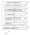
本発明の例示的実施形態が、図面に図示してある。図1、図6、図10、図13、図15は、マイクロ波回路を作成する様々な方法を示す。以下の説明を読むことで明らかになる如く、本方法は様々な方法と組み合わせることができる。 Exemplary embodiments of the invention are illustrated in the drawings. 1, 6, 10, 13, and 15 illustrate various methods of creating a microwave circuit. As will become apparent upon reading the following description, the method can be combined with various methods.
マイクロ波回路を作成する第1の方法が、図1に示してある。一般に、本方法100は接地面を覆って厚膜誘電体を付着(102)し、続いて厚膜誘電体上に導体を形成(104)するステップを含む。厚膜誘電体は、基板を覆って第1の厚膜誘電体層を付着(106)し、続いてこの層を空気乾燥(108)して溶剤を脱気し、それによって層の多孔性を増すことで形成する。次に、この層を150℃で炉内乾燥(110)する。第1の層を付着して乾燥させた後、追加の厚膜誘電体層を第1の層の上面に付着(112)する。最後の層を含め各追加の層を付着した後、層を炉内乾燥する。全ての層を付着して炉内乾燥させた後、堆積層を焼成(114)する。
A first method of creating a microwave circuit is shown in FIG. In general, the
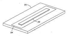
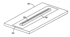
図2乃至図4は、上記方法の例示的応用分野を示す。図2は、例えば40ミル(1.016ミリ)のラップ仕上げした酸化アルミニウムセラミック基板でもよい基板200を示す。基板200は、その上面に接地面204を備える。しかしながら、接地面は基板の底面や或いは基板内部にさえ設けることもできる。本説明の目的上、用語「接地面」は、1以上の特定の導体について接地面として機能する接地トレースだけでなく、基板を実質的に或いは完全に被覆する接地面をも包含することを意図するものである。
2 to 4 show an exemplary field of application of the method. FIG. 2 shows a
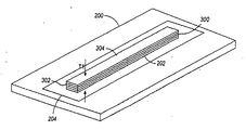
図1の方法によれば、第1の厚膜誘電体層202を接地面204を覆って付着する。一実施形態では、誘電体202はヘレイオス(Heraeus)社(米国ペンシルバニア州ウェストコンショーケン、ユニオンヒル通り24番地)から入手可能なKQCL−90−7858誘電体(ガラス誘電体)である。しかしながら、誘電体202は別の誘電体とすることもでき、特に別のKQ誘電体やガラス誘電体や適当な電気的特性を有する他の誘電体とすることもできる。
In accordance with the method of FIG. 1, a first thick film
標準的な厚膜ペーストに似たKQCL−90−7858印刷は、(酸化アルミニウムセラミックに関する9.6とは対照的に)3.95の誘電定数を有し、2E−4の誘電正接を有し、従来のベルト炉内で空気中で850℃で焼成してもよく、焼成後に光学的に透明とされ、デュポン社(米国デラウェア州ウィルミントン、マーケット街1007番地)から入手可能なデュポンQG150金と互換性がある。KQCL−90−7858の低損失及び低誘電率は、マイクロ波回路(例えば、マイクロ波伝送線路)の形成に特に適したものである。 KQCL-90-7858 printing, similar to a standard thick film paste, has a dielectric constant of 3.95 (as opposed to 9.6 for aluminum oxide ceramics) and a dielectric tangent of 2E-4 Dupont QG150 gold, which may be fired in air in a conventional belt furnace at 850 ° C., made optically transparent after firing and available from DuPont (1007 Market Street, Wilmington, Delaware, USA) Compatible. The low loss and low dielectric constant of KQCL-90-7858 are particularly suitable for forming microwave circuits (eg, microwave transmission lines).
KQCL−90−7858は、スクリーン印刷を介して基板200/204上に付着させることができる。実際には、付着前にKQCL−90−7858を180±2.0の粘度に薄くしてから、それをステンレス鋼スクリーン(例えば、200メッシュ、1.6ミルワイヤ、0.8ミル乳剤)を介して印刷することが有益であることが分かっている。
KQCL-90-7858 can be deposited on the
付着誘電体層202を直ちに炉内乾燥した場合、乾燥するにつれてそれがひび割れしがちとなる。これは、誘電体層内部に異常な圧力を生成する気体が捕捉されている結果と考えられる。しかしながら、誘電体層の乾燥を引き延ばすことで溶剤を層から脱気し、それによって層の多孔性が増すことが発見されている。金メッキを施した酸化アルミニウムセラミック基板上に付着させ、約1.5ミル(0.0381ミリ)の乾式印刷の厚さを持たせた第1のKQCL−90−7858誘電体層にとって、少なくとも45分間の空気乾燥は層を炉内乾燥させたときにひび割れを軽減する傾向がある。空気乾燥に続き、層202は標準的な炉による乾燥(例えば、約150℃のピーク温度での約15分間の炉内乾燥)にさらすことができる。
If the deposited
第1の厚膜誘電体層202の空気乾燥及び炉内乾燥後に、追加の厚膜誘電体層300,302,304を第1層の上面に(例えば、基板上に第1の厚膜誘電体層を付着させるのに用いるのと同じ手順を用い、図3参照)付着させることができる。各連続層は、次の層の付着前に約5分間の素早い炉内乾燥にさらすことができる。乾燥はさせたが焼成はしていない第1の誘電体層を基板200/204よりも実質的により多孔質とし、同様の組成である追加の誘電体層300〜304が第1の層202と基板200/204の間の結合よりも互いに強固な結合を形成する傾向があるとすると、追加の厚膜誘電体層の空気乾燥の引き延ばしは通常不要であり、製造工程を短縮するのに省くことができる。
After air drying and in-furnace drying of the first thick film
全ての厚膜誘電体層202、300〜304を付着し乾燥させた後、これらの層を焼成する(図4の焼成誘電体参照のこと)。KQCL−90−7858誘電体で層構成した場合、焼成は一般に用いられる厚膜焼成サイクルを用いて実行することができる(例えば、この層は最大で約10分の休止に対し約850℃の最大温度で従来のベルト炉にて空気焼成することができる。適切に脱気して全ての有機材料を焼き尽くすには、制御された緩慢な昇温を導入するとよい。同様に、基板の破損を防ぐのに制御された緩慢な降温を用いることができる)。
After all thick film
焼成期間中、付着させた誘電体層202,300〜304は(溶剤と有機結合体の燃え尽きることが原因で)収縮する。その結果、所望の最終的な誘電体の肉厚(すなわち図4の「焼成印刷肉厚」T2)は、十分な誘電体層202,300〜304を付着させて所望の最終的な誘電体肉厚を超える乾式印刷肉厚(図3のT1)を獲得することでのみ達成することができる。一例を挙げれば、前述のKQCL−90−7858は焼成時に元々の非焼成肉厚(厚さ)の約60%まで収縮することになる。他の誘電体はこれよりも大きいか又はより小さな収縮率を有するが、この収縮率は一般に所与の製造者の特定の製品種について一貫したものとなろう。堆積層の乾式印刷肉厚(厚さ)と焼成印刷肉厚(厚さ)は共に、ドロップゲージ測微計やスタイラス側面計を用いて計測することができる。
During the firing period, the deposited
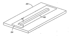
厚膜層の付着期間中に厚膜層の高さを正確に制御する仕方には限界が存在するため、かつ連続する厚膜層の付着が厚膜高さの変動の影響を倍増するだけであるため、場合によっては所望の乾式印刷肉厚を超える乾式印刷肉厚(T1)が達成されるまで厚膜誘電体層を付着することが望ましい。正確な最終的な誘電体の肉厚(T2)は、そこで様々な方法で達成することができる。一つの方法は、堆積層を焼成する前に堆積層202,300〜304を所望の乾式印刷肉厚まで平坦化し、その最終結果を得るべく既知の収縮率を用いるものである。この場合、有用な等式は「乾式印刷肉厚=焼成印刷肉厚/収縮係数」である。注意深く単純な切抜き金属シムパターンを用い、10ミル(0.254ミリ)肉厚誘電体に対し±0.1ミル(0.00254ミリ)よりも良好な最終肉厚を得ることができる。より高価ではあるがより正確な方法は、焼成した層を所望の最終的な誘電体肉厚にまで研磨することである。本方法を用いることで、10ミル(0.254ミリ)肉厚の誘電体層を±0.1ミル(0.00254ミリ)よりも優れたばらつきで制御することができる。次に、接地面を磨きあらゆる引っ掻き傷を除去するか、或いは誘電体がKQCL−90−7858である場合は、研磨した誘電体400を再焼成して接地面と端部を平滑化する(すなわち、KQCL−90−7858は再焼成時にリフローする傾向があるからである)。
There is a limit to how accurately the thickness of the thick film layer can be controlled during the thick film deposition period, and successive thick film deposition only doubles the effect of thick film thickness variation. Thus, in some cases, it may be desirable to deposit a thick dielectric layer until a dry print thickness (T1) that exceeds the desired dry print thickness is achieved. The exact final dielectric thickness (T2) can then be achieved in various ways. One method is to planarize the deposited
KQCL−90−7858誘電体については、研磨法を用いるときに約5ミル(0.127ミリ)の肉厚の最終(焼成)誘電体を得るのに約11ミル(0.2794ミリ)の乾式印刷肉厚が必要であることに留意されたい。 For the KQCL-90-7858 dielectric, about 11 mils (0.2794 mm) dry to obtain a final (fired) dielectric of about 5 mils (0.127 mm) thick when using the polishing method. Note that print wall thickness is required.
接地面204を覆って厚膜誘電体400を付着させた後、厚膜誘電体上に導体500を形成することができる(図5参照)。一例を挙げれば、この種の導体は誘電体400上に導電性厚膜を(例えば、スクリーン印刷やステンシルやドクターブレーディングを介して)付着し、続いて導電性厚膜内の導体をパターン形成してエッチングすることで形成することができる。あるいは、導体500は図6に示した方法に説明した如く形成することもできる。
After the
図6は、マイクロ波回路の第2の作成方法を示す。方法600は、接地面を覆って誘電体を付着(602)し、続いて誘電体上に導体を形成(604)するステップを含む。
FIG. 6 shows a second method for creating a microwave circuit.
導体は、誘電体上に導電性厚膜を付着(606)し、導電性厚膜の「半焼結」(608)により誘電体上に形成する。半焼結は、ここでは導電性厚膜の単純な「乾燥」温度を超える温度ながら、導電性厚膜に関して製造者が推奨する「焼成」温度未満の温度にて実行する加熱工程として規定される。 The conductor is formed on the dielectric by depositing a conductive thick film on the dielectric (606) and "semi-sintering" the conductive thick film (608). Semi-sintering is defined herein as a heating step that is performed at a temperature below the simple “drying” temperature of the conductive thick film, but below the “baking” temperature recommended by the manufacturer for the conductive thick film.
所定の誘電体上に所定の導電性厚膜を付着させると、導電性厚膜は誘電体と反応し、ラップ仕上げした酸化アルミニウムセラミック等の基板上に同じ導電性厚膜を付着させる場合よりもエッチングがより困難な境界層を生成する。しかしながら、半焼結を行うことにより化学的エッチングで首尾よくパターン形成することのできる導電性厚膜を生成することが分かっている。半焼結雰囲気と温度と時間は、不要な有機材料を取り除き焼却するのに十分で、完全に緻密化されていないコヒーレント導電膜を形成するのに十分でなければならない。上述の境界層の有害な影響は、半焼結により大幅に低減される。 When a predetermined conductive thick film is deposited on a predetermined dielectric, the conductive thick film reacts with the dielectric, compared to a case where the same conductive thick film is deposited on a substrate such as a lapped aluminum oxide ceramic. Produces a boundary layer that is more difficult to etch. However, it has been found that semi-sintering produces a conductive thick film that can be successfully patterned by chemical etching. The semi-sintered atmosphere, temperature and time must be sufficient to remove and burn out unwanted organic materials and to form a coherent conductive film that is not fully densified. The detrimental effects of the boundary layer described above are greatly reduced by semi-sintering.
半焼結は、化学的エッチングに対し十分な抵抗性があって境界層の範囲を最小化する一方で良好なパターン画成を可能にする導電性厚膜層を生成する。実際の境界層の形成は、時間と温度に高度に依存する複雑なソリッドステート拡散メカニズムによって決まる。境界層の範囲を最小化することで、導電性厚膜内にパターン化した一つの導体(又は複数の導体)を不要に過剰エッチングする前に同じエッチング工程にてそれを取り除くことができる。 Semi-sintering produces a conductive thick film layer that is sufficiently resistant to chemical etching to minimize boundary layer coverage while allowing good pattern definition. The actual boundary layer formation depends on a complex solid state diffusion mechanism that is highly time and temperature dependent. By minimizing the range of the boundary layer, one conductor (or multiple conductors) patterned in the conductive thick film can be removed in the same etching step before unnecessarily overetching.
半焼結の前又は後に、導電性厚膜をパターン形成(610)し、一つ(又は複数)の導体を画成する。半焼結後、導電性厚膜をエッチング(612)し、一つ(又は複数)の導体を露出させる。次に、一つ(又は複数)の導体を全焼結温度にて焼成(614)する。 Before or after semi-sintering, the conductive thick film is patterned (610) to define one (or multiple) conductors. After semi-sintering, the conductive thick film is etched (612) to expose one (or more) conductors. Next, one (or more) conductors are fired (614) at the total sintering temperature.
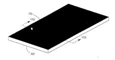
図4及び図7乃至図9は、上記方法の例示的な応用分野を示す。図4は、基板200を示し、例えばラップ仕上げした40ミルの酸化アルミニウムセラミック基板でもよい。誘電体400を様々な構造のうちの任意のもので基板200上に付着させるが、一例を挙げれば、多少とも台形断面を有する長く幅狭の盆を形成してもよい。図8を参照されたい。一実施形態では、誘電体はKQCL−90−7858である。しかしながら、誘電体は別の誘電体としてもよく、特に別のKQ誘電体やガラス誘電体や適当な電気的特性を有する他の誘電体とすることができる。
4 and 7-9 show exemplary application areas of the method. FIG. 4 shows a
図7及び図8に示す如く、導電性厚膜700を誘電体400上に付着させる。この厚膜700は、スクリーン印刷やステンシル印刷やドクターブレーディングを含む幾つかの方法で付着させることができる。一実施形態では、導電性厚膜はデュポンQG150等の金からなる。
As shown in FIGS. 7 and 8, a conductive
導電性厚膜700は誘電体400上に単独で付着させるか、或いは図7に示した如く誘電体400と基板200の双方の一部を覆って付着させることができる。前述の如く、一部の導電性厚膜はそれを付着させた誘電体と反応し、それによって導電性厚膜700と誘電体400の間に境界層800を生成し、それはラップ仕上げした酸化アルミニウムセラミック等の基板上に同じ導電性厚膜を付着させる場合はエッチングがより困難である。この種の境界層800は、デュポンQG150をKQCL−90−7858上に付着させたときに形成される。この境界層800は図8に最もよく図示してあり、同図は図7に示した誘電体400と導電性厚膜700の断面を示すものである。
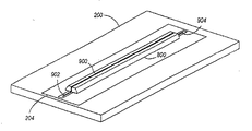
The conductive
導体をKQCL−90−7858上に付着させた直後にデュポンQG150にパターン形成しエッチングした場合、境界層800のエッチングに必要な時間は十分長く、パターン形成した導体の不要なエッチングが起きることもある。すなわち、そのエッチング時間は十分に長く、パターン形成した導体の壁と端部は腐食し始め、恐らくは導体の所望のインピーダンスを変更しよう。不要な導体エッチングの影響は、A)導電性厚膜700を2以上の異なる材料上に付着したり、B)導電性厚膜が材料の一つをより素早くエッチングする傾向があるときに複合されよう。例えば、酸化アルミニウムセラミック基板上に付着させたデュポンQG150は、KQCL−90−7858上に付着させたデュポンQG150よりも素早くエッチングする。
When a DuPont QG150 is patterned and etched immediately after the conductor is deposited on KQCL-90-7858, the time required for etching the
上記段落に言及した問題は、エッチング前に導電性厚膜700を「半焼結」させることで緩和することができる。前述の如く、半焼結は、導電性厚膜の単なる「乾燥」温度よりも大きな温度ではであるものの、導電性厚膜について製造者が推奨する「焼成」温度未満の温度にて行われる加熱工程である。KQCL−90−7858上に付着させたデュポンQG150にとっては、725℃と850℃の間のピーク温度における半焼成が有効であることが分かっており、約10分に亙る約725℃のピーク温度における半焼成が最も有効であることが分かっている。
The problems mentioned in the above paragraph can be mitigated by “semi-sintering” the conductive
導電性厚膜700を半焼成した後、それは化学的エッチングに対し十分に抵抗性があり、それによって導電性厚膜700内にパターン形成する任意の導体900,902,904の不要な過剰エッチング前に境界層800がエッチングできるようになる。適当な時間と温度で半焼成することは、二つの異なる材料(例えば、酸化アルミニウムセラミックやKQCL−90−7858)上に付着した導電性厚膜のエッチング比を等化させるのにも役立つ。
After semi-baking the conductive
導体900〜904は半焼結の前か後に導電性厚膜700にてパターン形成し、半焼成後に導電性厚膜700をエッチング(例えば、化学的エッチング)して一つ(又は複数)の導体を露出させることができる。図9を参照されたい。エッチングとあらゆる必要な清掃(例えば、洗浄と濯ぎ)の後に、露出導体900〜904を焼成する。デュポンQG150導体については、約850℃のピーク温度において焼成を施すことができる。
The
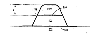
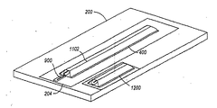
図10は、マイクロ波回路のさらに別の作成方法を示す。本方法1000は、接地面204を覆う第1の誘電体400の付着(1002)に始まり、続いて誘電体400(図11)上に導体900を形成(1004)する。第1の誘電体と導体は厚膜(恐らく多層厚膜)とされようが、これに限るものではない。
FIG. 10 shows still another method of creating a microwave circuit. The
第1の誘電体と導体の付着に続き、導体900のインピーダンスを計測(1006)し、計測したインピーダンスと所望のインピーダンスを用いて第2の厚膜誘電体の乾式印刷肉厚(図11のT3)について解く。次に、導体900と第1の導体400を覆って第2の厚膜誘電体1100を付着(1008)し、それによって第1と第2の誘電体400,1100の間に導体900を封入する。次に接地シールド層1102が、第1と第2の誘電体を覆って形成(1010)される。随意選択的ではあるが、接地シールド層1102を接地面204に導電結合させることができる。
Following the adhesion of the first dielectric and the conductor, the impedance of the
図10の方法の一実施形態では、第1と第2の誘電体は図1の方法により付着させる厚膜誘電体であり、導体は図6の方法により付着する厚膜導体である。 In one embodiment of the method of FIG. 10, the first and second dielectrics are thick film dielectrics deposited by the method of FIG. 1, and the conductor is a thick film conductor deposited by the method of FIG.
導体900のインピーダンスは、時間領域反射率測定により計測することができる。実際の回路上の導体のインピーダンスは導体自体から計測できるが、導体或いは囲繞導体の構造は導体のインピーダンスの直接計測を困難にするものとなろう。或いは、例えば異なるデバイス上の導体の異なる配置がインピーダンス計測デバイスをして異なる構造のインピーダンスの計測を困難にすることがある。それ故、マイクロ波回路の形成に用いるのと同じ工程を用いてマイクロ波回路と同時に試験構造体1200を形成し、続いて試験構造体1200のインピーダンスを計測し、導体900のインピーダンスが同一であると仮定することは有益である。この種の試験構造体が、図12に示してある。
The impedance of the
導体900の被計測インピーダンスが所望のインピーダンス未満である場合は、第2の厚膜誘電体1100の焼成印刷肉厚を第1の厚膜誘電体400の焼成印刷肉厚よりも厚く作成しなければならない。同様に、計測したインピーダンスが所望のインピーダンスよりも大きい場合は、第2の厚膜誘電体1100の焼成印刷肉厚は第1の厚膜誘電体400の焼成印刷肉厚よりも薄くしなければならない。一般に、第2の誘電体1100の肉厚は計測したインピーダンスの所望インピーダンスからの偏差割合の2倍でもって調整することができる。次に第2の誘電体1100に関する適当な「乾式印刷」肉厚を前述の収縮率の考察或いはより精密な肉厚研磨方法を用いるかどうかにより決定することができる。電磁界−解明ソフトウェアプログラムを、必要な焼成印刷肉厚の割り出しに用いることができる。この種の二つのプログラムは「HFSS;High Frequency Structure Simulator(高周波構造シミュレータ)」、すなわちアジレント・テクノロジーズ(Agilent Technologies)社(米国カリフォルニア州パロアルト、ペイジミル通り395番地)から入手可能な完全三次元UNIXベースプログラムと、ポーラー・インストルメント(Polar Instruments)社(米国カリフォルニア州サンマテオ、イーストベルビュー通り320番地)から入手可能な「Si8000」である。
If the measured impedance of the
図13は、マイクロ波回路の第4の作成方法を示す。図10の方法の如く、方法1300は接地面204を覆う第1の誘電体の付着(1302)に始まり、誘電体400上の導体900の形成(1304)が続く(図11)。次に第2の誘電体1100を導体900と第1の誘電体400を覆って付着(1300)させ、それによって第1と第2の誘電体の間に導体を封入する。第1と第2の誘電体は、導体と同様、厚膜(と、恐らくは多層厚膜)とすることができるが、これに限るものではない。
FIG. 13 shows a fourth method for creating a microwave circuit. Like the method of FIG. 10, the
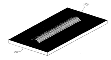
誘電体400,1100と導体900を付着させた後、第1と第2の誘電体400,1100を覆って接地シールド層1102を形成(1308)し、接地面204に導電結合させることができる。接地シールド層1102は、1)第1及び第2の誘電体を(エレクトロサイエンス・ラボラトリーズ(Electro−Science Laboratories)社(米国ペンシルバニア州キングオブプルシャ、イーストチャーチ通り416番地)から入手可能なESL8081−A等の)有機金属層で予被覆(1310)し、2)予被覆層を覆って厚膜接地シールド層を付着(1312)することで、形成することができる。接地シールド層1102は、誘電体400,1100を覆ってポリマースクリーン1400(図14)を配置し、それが誘電体の輪郭に少なくとも一部合致するまでポリマースクリーンに圧力を作用させることで予被覆層を覆って付着させることができる。次に厚膜接地シールド層1102は、ポリマースクリーン1400を介して印刷することができる。
After the
図13の方法の一実施形態では、第1と第2の誘電体は図1の方法に従って付着させた厚膜誘電体であり、導体は図6の方法に従って付着させた厚膜導体である。 In one embodiment of the method of FIG. 13, the first and second dielectrics are thick film dielectrics deposited according to the method of FIG. 1, and the conductor is a thick film conductor deposited according to the method of FIG.
図13の方法は、第2の厚膜誘電体を付着する前に、導体900のインピーダンスを計測するステップと、計測したインピーダンスと所望のインピーダンスを用いて第2の厚膜誘電体の乾式印刷肉厚に関する等式を解くステップをさらに含んでもよい。
The method of FIG. 13 includes the steps of measuring the impedance of the
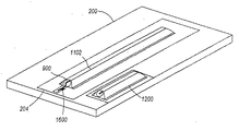
図15は、マイクロ波回路の第5の作成方法を示す。本方法1500は、接地面204を覆う第1の誘電体の付着(1502)に始まり、誘電体上に導体900を形成すること(1504)が続く(図16)。続いて導体と第1の誘電体を覆って第2の誘電体を付着(1506)させ、それによって第1と第2の誘電体の間に導体を封入する。第1と第2の誘電体は、導体と同様に厚膜(と恐らくは多層厚膜)とすることができるが、これに限るものではない。
FIG. 15 shows a fifth method of creating a microwave circuit. The
誘電体と導体を付着した後、第1と第2の誘電体を覆って接地シールド層1102を形成(1508)する。接地シールド層は、誘電体を覆ってポリマースクリーン1400(図14)を配置1510し、それが誘電体の輪郭に少なくとも一部合致するまでポリマースクリーンに圧力を作用させることで付着させることができる。次に厚膜接地シールド層1102をポリマースクリーン1400を介して印刷することができる。
After attaching the dielectric and the conductor, a
図15の方法の一実施形態では、第1及び第2の誘電体は図1の方法に従って付着させる厚膜誘電体であり、導体は図6の方法に従って付着させる厚膜導体である。 In one embodiment of the method of FIG. 15, the first and second dielectrics are thick film dielectrics deposited according to the method of FIG. 1, and the conductor is a thick film conductor deposited according to the method of FIG.
図15の方法は、第2の厚膜誘電体を付着する前に、導体900のインピーダンスを計測するステップと、計測したインピーダンスと所望のインピーダンスを用いて第2の厚膜誘電体の乾式印刷肉厚に関する等式を解くステップをさらに含んでもよい。
The method of FIG. 15 includes the steps of measuring the impedance of the
先に触れた如く、図1、図6、図10、図13、図15に示した方法のうちの任意のもの或いは全てを組み合わせることができる。さらに、どの方法も、1)一つ(又は複数)の誘電体を覆ってポリマースクリーンを配置し、2)それが一つ(又は複数)の誘電体の輪郭に少なくとも一部が合致するまでポリマースクリーンに圧力を作用させ、次に3)ポリマースクリーンを介して厚膜抵抗体1600を印刷することで、一つ(又は複数)の誘電体の近傍に厚膜抵抗体1600を形成するステップをさらに含めることができる。図16を参照するに、これは厚膜抵抗体1600を示すが、それを介して印刷するポリマースクリーンは示していない。ポリマースクリーンは、異なる形状を有するも、図1に示したスクリーン1400に類似したものとなろう。
As previously mentioned, any or all of the methods shown in FIGS. 1, 6, 10, 13, and 15 can be combined. Further, all methods include 1) placing a polymer screen over one (or more) dielectrics, and 2) polymer until it at least partially matches the contour of one (or more) dielectrics. Applying a pressure to the screen, and then 3) printing the
ポリマースクリーンは、今日の製造工程ではステンレス鋼スクリーンに大幅に置き換わっているが、ポリマースクリーンに対し圧力を作用させ、誘電体の輪郭に幾分か合致するようにさせ、かくして接地シールド層或いは厚膜抵抗体を印刷しようとする面に対し面一に(或いは少なくとも密接して)着座しないスクリーンを介して厚膜抵抗体の接地シールド層を印刷することに関連する厚さと整列ずれの懸念を緩和する点において、ポリマースクリーンは起立する誘電体の上部/近傍の接地シールド層或いは厚膜抵抗体の印刷に特に有用である。厚膜抵抗体は急峻な誘電体(すなわち、関連表現ではスティープ)を横臥させる前に印刷することもできるが、そうすることが抵抗体を高温での反復焼成にさらし、その意図した値から受け入れ難いずれを招くことがある。 While polymer screens are a significant replacement for stainless steel screens in today's manufacturing processes, pressure is applied to the polymer screen to make it somewhat conform to the contour of the dielectric, and thus a ground shield layer or thick film. Reduces thickness and misalignment concerns associated with printing a thick film resistor ground shield layer through a screen that does not sit flush (or at least in close proximity) to the surface on which the resistor is to be printed. In that respect, polymer screens are particularly useful for printing a ground shield layer or thick film resistor on / near an upstanding dielectric. Thick film resistors can also be printed before lying down a steep dielectric (ie steep in related terms), but doing so exposes the resistor to repeated firing at high temperatures and accepts it from its intended value. It may cause difficulties.
上記の説明を読んだ後で当業者には理解される如く、図1,6,10,13,15に示した方法を用い、伝送線路をマイクロストリップやストリップ線路や同一平面上の同軸線路及び/又は準同軸線路(すなわち、同軸線路ではあるが断面対称性が欠如)の構成に用いることができる。より薄肉でより幅狭の誘電体がより幅狭の導体に帰結し、かくしてより導体損失が増えるという但し書き付きで、製造工程が許す限り伝送線路を薄肉で幅狭に作成することができる。 As will be appreciated by those skilled in the art after reading the above description, the transmission lines may be microstrip, stripline, coplanar coaxial lines and the like, using the method shown in FIGS. It can be used for the construction of a quasi-coaxial line (that is, a coaxial line but lacks cross-sectional symmetry). With the proviso that thinner and narrower dielectrics result in narrower conductors, thus increasing conductor losses, transmission lines can be made as thin and narrow as the manufacturing process allows.
以上本発明の各実施例について説明したが、実施例の理解を容易にするために、実施例ごとの要約を以下に列挙する。
〔1〕 マイクロ波回路の作成方法(100)であって、
a)接地面を覆って厚膜誘電体を付着(102)するステップで、
i)前記接地面を覆って第1の厚膜誘電体層を付着(106)し、
ii)前記第1の層を乾燥(108)させて溶剤を脱気し、それによって前記第1の層の多孔性を増し、
iii)前記第1の層を炉内乾燥(110)し、
iv)前記第1の層の上面に追加の厚膜誘電体層を付着(112)し、該各層の付着後に炉内乾燥させ、
v)前記付着層を焼成(114)する、
ことによるステップ(102)と、
b)前記厚膜誘電体上に導体を形成(104)するステップを有する、
ことを特徴とするマイクロ波回路の作成方法(100)。
〔2〕 前記厚膜誘電体近傍に厚膜抵抗体を形成(1508)するステップで、
a)前記厚膜誘電体を覆ってポリマースクリーンを配置(1510)し、前記厚膜誘電体の輪郭に少なくとも一部合致するまで前記ポリマースクリーンに圧力を作用させ、
b)前記ポリマースクリーンを介して前記厚膜抵抗体を印刷(1512)する、
ことによるステップ(1508)をさらに備える、
ことを特徴とする〔1〕記載のマイクロ波回路の作成方法(100)。
〔3〕 マイクロ波回路を作成する方法(600)であって、
a)接地面を覆って誘電体を付着(602)するステップと、
b)前記誘電体上に導体を形成(604)するステップで、
i)前記誘電体上に導電性厚膜を付着(606)し、
ii)前記導電性厚膜を半焼結(608)させ、
iii)前記導電性厚膜をパターン形成(610)して少なくとも一つの導体を画成し、
iv)半焼結後に、前記導電性厚膜をエッチング(612)して前記少なくとも一つの導体を露出させ、
v)全焼結温度にて前記露出させた少なくとも一つの導体を焼成(614)する、
ことによるステップ(604)を有する、
ことを特徴とするマイクロ波回路の作成方法(600)。
〔4〕 前記誘電体は、
a)接地面を覆って第1の厚膜誘電体層を付着(106)するステップと、
b)前記第1の層を空気乾燥(108)して溶剤を脱気し、それによって前記第1の層の多孔性を増大させるステップと、
c)前記第1の層を炉内乾燥(110)するステップと、
d)前記第1の層の上面に追加の厚膜誘電体層を付着(112)し、各追加層の付着後に炉内乾燥させるステップと、
e)堆積層を焼成(114)するステップを含む、
ことを特徴とする〔3〕記載のマイクロ波回路の作成方法(600)。
〔5〕 前記ガラス誘電体近傍に厚膜抵抗体を形成(1508)するステップで、
a)前記ガラス誘電体を覆ってポリマースクリーンを配置(1510)し、前記ガラス誘電体の輪郭に少なくとも一部合致するまで前記ポリマースクリーンに圧力を作用させ、
b)前記ポリマースクリーンを介して前記厚膜抵抗体を印刷(1512)する、
ことによるステップをさらに有する、
ことを特徴とする〔3〕記載のマイクロ波回路の作成方法(600)。
〔6〕 マイクロ波回路を作成する方法(1000)であって、
a)接地面を覆って第1の誘電体を付着(1002)するステップと、
b)前記第1の誘電体上に導体を形成(1004)するステップと、
c)前記導体のインピーダンスを計測(1006)し、該計測したインピーダンスと所望のインピーダンスを用いて、第2の厚膜誘電体の乾式印刷の厚さに関する等式を解くステップと、
d)前記導体及び前記第1の誘電体を覆って前記第2の厚膜誘電体を付着(1008)し、それによって前記第1と第2の誘電体の間に導体を封入するステップと、
e)前記第1及び第2の誘電体を覆って接地シールド層を形成(1010)するステップを有する、
ことを特徴とするマイクロ波回路の作成方法(1000)。
〔7〕 前記インピーダンス計測は、時間領域反射率測定を用いて実行する、ことを特徴とする〔6〕記載の方法(1000)。
〔8〕 前記インピーダンス計測は、マイクロ波回路を形成するのと同じ工程を用い、マイクロ波回路と並列に形成する試験構造体(1200)上で実行する、
ことを特徴とする〔6〕記載のマイクロ波回路の作成方法(1000)。
〔9〕 前記第1の誘電体は厚膜誘電体である、
ことを特徴とする〔6〕記載のマイクロ波回路の作成方法(1000)。
〔10〕a)前記導体の計測インピーダンスが前記所望インピーダンスに満たない場合は、前記第2の厚膜誘電体の乾式印刷の厚さを前記第1の厚膜誘電体の乾式印刷の厚さよりも厚くし、
b)前記導体の計測インピーダンスが前記所望インピーダンスを超える場合は、前記第2の厚膜誘電体の乾式印刷の厚さを前記第1の厚膜誘電体の乾式印刷の厚さよりも薄くする、
ことを特徴とする〔9〕記載のマイクロ波回路の作成方法(1000)。
Although each embodiment of the present invention has been described above, in order to facilitate understanding of the embodiment, a summary for each embodiment is listed below.
[1] A method (100) of creating a microwave circuit,
a) depositing (102) a thick film dielectric over the ground plane;
i) depositing (106) a first thick film dielectric layer over the ground plane;
ii) drying (108) the first layer to degas the solvent, thereby increasing the porosity of the first layer;
iii) oven drying (110) the first layer;
iv) deposit (112) an additional thick film dielectric layer on top of the first layer, and dry in the furnace after the deposition of each layer;
v) firing (114) the adhesion layer;
Possibly step (102);
b) forming (104) a conductor on the thick film dielectric;
A method (100) for producing a microwave circuit,
[2] forming (1508) a thick film resistor in the vicinity of the thick film dielectric;
a) placing (1510) a polymer screen over the thick film dielectric and applying pressure to the polymer screen until it at least partially matches the contour of the thick film dielectric;
b) printing (1512) the thick film resistor through the polymer screen;
Further comprising an optional step (1508),
A method (100) for producing a microwave circuit as set forth in [1].
[3] A method (600) of creating a microwave circuit,
a) depositing (602) a dielectric over the ground plane;
b) forming (604) a conductor on the dielectric;
i) depositing (606) a conductive thick film on the dielectric;
ii) semi-sintering (608) the conductive thick film;
iii) patterning (610) the conductive thick film to define at least one conductor;
iv) After semi-sintering, etch (612) the conductive thick film to expose the at least one conductor;
v) firing (614) the at least one exposed conductor at a total sintering temperature;
Having an optional step (604),
A method of creating a microwave circuit (600).
[4] The dielectric is
a) depositing (106) a first thick film dielectric layer over the ground plane;
b) air drying (108) the first layer to degas the solvent, thereby increasing the porosity of the first layer;
c) drying (110) the first layer in a furnace;
d) depositing (112) additional thick film dielectric layers on top of said first layer and drying in the furnace after deposition of each additional layer;
e) firing (114) the deposited layer;
A method (600) for creating a microwave circuit as set forth in [3].
[5] In the step of forming (1508) a thick film resistor in the vicinity of the glass dielectric,
a) placing (1510) a polymer screen over the glass dielectric and applying pressure to the polymer screen until it at least partially matches the contour of the glass dielectric;
b) printing (1512) the thick film resistor through the polymer screen;
Further comprising an optional step,
A method (600) for creating a microwave circuit as set forth in [3].
[6] A method (1000) of creating a microwave circuit,
a) depositing (1002) a first dielectric over the ground plane;
b) forming (1004) a conductor on the first dielectric;
c) measuring (1006) the impedance of the conductor, and using the measured impedance and the desired impedance, solving an equation for dry printing thickness of the second thick film dielectric;
d) depositing (1008) the second thick film dielectric over the conductor and the first dielectric, thereby encapsulating the conductor between the first and second dielectrics;
e) forming (1010) a ground shield layer over the first and second dielectrics;
A method for producing a microwave circuit (1000).
[7] The method (1000) according to [6], wherein the impedance measurement is performed using time domain reflectivity measurement.
[8] The impedance measurement is performed on a test structure (1200) formed in parallel with the microwave circuit using the same process as that for forming the microwave circuit.
[6] The method for producing a microwave circuit according to [6] (1000).
[9] The first dielectric is a thick film dielectric.
[6] The method for producing a microwave circuit according to [6] (1000).
[10] a) When the measured impedance of the conductor is less than the desired impedance, the dry printing thickness of the second thick film dielectric is set to be larger than the dry printing thickness of the first thick film dielectric. Thicken,
b) if the measured impedance of the conductor exceeds the desired impedance, the dry printing thickness of the second thick film dielectric is made thinner than the dry printing thickness of the first thick film dielectric;
[9] The method for producing a microwave circuit according to [9] (1000).
例示的かつ現時点で好適な本発明の実施形態をここに詳細に説明してきたが、発明概念は別様に様々に実施し採用することができ、添付の特許請求の範囲が従来技術により限定されるものを除き、この種の変形を包含するものと解釈すべきことを意図するものであることは理解されたい。 While exemplary and presently preferred embodiments of the present invention have been described in detail herein, the inventive concept can be implemented and employed in various different ways, and the appended claims are limited by the prior art. It should be understood that except what is intended to be construed as encompassing this type of variation.
200 基板
202 第1の厚膜誘電体
204 接地面
300,302,304 厚膜誘電体層
400 厚膜誘電体
500 導体
700 導電性厚膜
800 境界層
900,902,904 導体
1100 第2の誘電体
1102 接地シールド層
1200 試験構造体
1400 ポリマースクリーン
1600 厚膜抵抗体
200
Claims (10)
a)接地面を覆って厚膜誘電体を付着するステップで、
i)前記接地面を覆って第1の厚膜誘電体層を付着し、
ii)前記第1の層を乾燥させて溶剤を脱気し、それによって前記第1の層の多孔性を増し、
iii)前記第1の層を炉内乾燥し、
iv)前記第1の層の上面に追加の厚膜誘電体層を付着し、該各層の付着後に炉内乾燥させ、
v)前記付着層を焼成する、
ことによるステップと、
b)前記厚膜誘電体上に導体を形成するステップを有する、
ことを特徴とするマイクロ波回路の作成方法。 A method of creating a microwave circuit,
a) depositing a thick film dielectric over the ground plane;
i) depositing a first thick dielectric layer over the ground plane;
ii) drying the first layer to degas the solvent, thereby increasing the porosity of the first layer;
iii) drying the first layer in a furnace;
iv) depositing additional thick film dielectric layers on top of the first layer, drying in the furnace after the deposition of each layer;
v) firing the adhesive layer;
Step by step,
b) forming a conductor on the thick film dielectric;
A method for producing a microwave circuit.
a)前記厚膜誘電体を覆ってポリマースクリーンを配置し、前記厚膜誘電体の輪郭に少なくとも一部合致するまで前記ポリマースクリーンに圧力を作用させ、
b)前記ポリマースクリーンを介して前記厚膜抵抗体を印刷する、
ことによるステップをさらに備える、
ことを特徴とする請求項1に記載のマイクロ波回路の作成方法。 Forming a thick film resistor in the vicinity of the thick film dielectric;
a) placing a polymer screen over the thick film dielectric and applying pressure to the polymer screen until it at least partially matches a contour of the thick film dielectric;
b) printing the thick film resistor through the polymer screen;
Further comprising an optional step,
The method for producing a microwave circuit according to claim 1.
a)接地面を覆って誘電体を付着するステップと、
b)前記誘電体上に導体を形成するステップで、
i)前記誘電体上に導電性厚膜を付着し、
ii)前記導電性厚膜を半焼結させ、
iii)前記導電性厚膜をパターン形成して少なくとも一つの導体を画成し、
iv)半焼結後に、前記導電性厚膜をエッチングして前記少なくとも一つの導体を露出させ、
v)全焼結温度にて前記露出させた少なくとも一つの導体を焼成する、
ことによるステップを有する、
ことを特徴とするマイクロ波回路の作成方法。 A method for creating a microwave circuit comprising:
a) depositing a dielectric over the ground plane;
b) forming a conductor on the dielectric,
i) depositing a conductive thick film on the dielectric;
ii) semi-sintering the conductive thick film;
iii) patterning said conductive thick film to define at least one conductor;
iv) After semi-sintering, the conductive thick film is etched to expose the at least one conductor;
v) firing the exposed at least one conductor at a total sintering temperature;
Having an optional step,
A method for producing a microwave circuit.
a)接地面を覆って第1の厚膜誘電体層を付着するステップと、
b)前記第1の層を空気乾燥して溶剤を脱気し、それによって前記第1の層の多孔性を増大させるステップと、
c)前記第1の層を炉内乾燥するステップと、
d)前記第1の層の上面に追加の厚膜誘電体層を付着し、各追加層の付着後に炉内乾燥させるステップと、
e)堆積層を焼成するステップを含む、
ことを特徴とする請求項3記載のマイクロ波回路の作成方法。 The dielectric is
a) depositing a first thick film dielectric layer over the ground plane;
b) air drying the first layer to degas the solvent, thereby increasing the porosity of the first layer;
c) oven drying the first layer;
d) depositing additional thick film dielectric layers on top of the first layer and drying in the furnace after deposition of each additional layer;
e) firing the deposited layer;
The method for producing a microwave circuit according to claim 3.
a)前記ガラス誘電体を覆ってポリマースクリーンを配置し、前記ガラス誘電体の輪郭に少なくとも一部合致するまで前記ポリマースクリーンに圧力を作用させ、
b)前記ポリマースクリーンを介して前記厚膜抵抗体を印刷する、
ことによるステップをさらに有する、
ことを特徴とする請求項3に記載のマイクロ波回路の作成方法。 Forming a thick film resistor in the vicinity of the glass dielectric;
a) placing a polymer screen over the glass dielectric and applying pressure to the polymer screen until it at least partially matches the contour of the glass dielectric;
b) printing the thick film resistor through the polymer screen;
Further comprising an optional step,
The method for producing a microwave circuit according to claim 3.
a)接地面を覆って第1の誘電体を付着するステップと、
b)前記第1の誘電体上に導体を形成するステップと、
c)前記導体のインピーダンスを計測し、該計測したインピーダンスと所望のインピーダンスを用いて、第2の厚膜誘電体の乾式印刷の厚さに関する等式を解くステップと、
d)前記導体及び前記第1の誘電体を覆って前記第2の厚膜誘電体を付着し、それによって前記第1と第2の誘電体の間に導体を封入するステップと、
e)前記第1及び第2の誘電体を覆って接地シールド層を形成するステップを有する、
ことを特徴とするマイクロ波回路の作成方法。 A method for creating a microwave circuit comprising:
a) depositing a first dielectric over the ground plane;
b) forming a conductor on the first dielectric;
c) measuring the impedance of the conductor, and using the measured impedance and the desired impedance, solving an equation relating to the dry printing thickness of the second thick film dielectric;
d) depositing the second thick film dielectric over the conductor and the first dielectric, thereby encapsulating the conductor between the first and second dielectrics;
e) forming a ground shield layer over the first and second dielectrics;
A method for producing a microwave circuit.
ことを特徴とする請求項6に記載のマイクロ波回路の作成方法。 The impedance measurement is performed on a test structure that is formed in parallel with the microwave circuit using the same process as that for forming the microwave circuit.
The method for producing a microwave circuit according to claim 6.
ことを特徴とする請求項6に記載のマイクロ波回路の作成方法。 The first dielectric is a thick film dielectric;
The method for producing a microwave circuit according to claim 6.
b)前記導体の計測インピーダンスが前記所望インピーダンスを超える場合は、前記第2の厚膜誘電体の乾式印刷の厚さを前記第1の厚膜誘電体の乾式印刷の厚さよりも薄くする、
ことを特徴とする請求項9に記載のマイクロ波回路の作成方法。 a) if the measured impedance of the conductor is less than the desired impedance, the thickness of the dry printing of the second thick film dielectric is greater than the thickness of the dry printing of the first thick film dielectric;
b) if the measured impedance of the conductor exceeds the desired impedance, the dry printing thickness of the second thick film dielectric is made thinner than the dry printing thickness of the first thick film dielectric;
The method for producing a microwave circuit according to claim 9.
Applications Claiming Priority (1)
| Application Number | Priority Date | Filing Date | Title |
|---|---|---|---|
| US10/600,143 US6953698B2 (en) | 2003-06-19 | 2003-06-19 | Methods for making microwave circuits |
Publications (2)
| Publication Number | Publication Date |
|---|---|
| JP2005012811A true JP2005012811A (en) | 2005-01-13 |
| JP2005012811A5 JP2005012811A5 (en) | 2007-07-12 |
Family
ID=33517678
Family Applications (1)
| Application Number | Title | Priority Date | Filing Date |
|---|---|---|---|
| JP2004180844A Pending JP2005012811A (en) | 2003-06-19 | 2004-06-18 | How to create a microwave circuit |
Country Status (4)
| Country | Link |
|---|---|
| US (3) | US6953698B2 (en) |
| JP (1) | JP2005012811A (en) |
| CN (1) | CN1574451A (en) |
| TW (1) | TWI232487B (en) |
Cited By (2)
| Publication number | Priority date | Publication date | Assignee | Title |
|---|---|---|---|---|
| WO2018020919A1 (en) * | 2016-07-29 | 2018-02-01 | 株式会社村田製作所 | Transmission line and electronic device |
| TWI732753B (en) * | 2015-05-13 | 2021-07-11 | 日商新力股份有限公司 | Transmission line |
Families Citing this family (23)
| Publication number | Priority date | Publication date | Assignee | Title |
|---|---|---|---|---|
| US7022251B2 (en) * | 2003-06-19 | 2006-04-04 | Agilent Technologies, Inc. | Methods for forming a conductor on a dielectric |
| US6953698B2 (en) * | 2003-06-19 | 2005-10-11 | Agilent Technologies, Inc. | Methods for making microwave circuits |
| WO2008021269A2 (en) * | 2006-08-11 | 2008-02-21 | E. I. Du Pont De Nemours And Company | Device chip carriers, modules, and methods of forming thereof |
| US8129266B2 (en) * | 2008-07-09 | 2012-03-06 | Semiconductor Componenets Industries, LLC | Method of forming a shielded semiconductor device and structure therefor |
| US8171617B2 (en) * | 2008-08-01 | 2012-05-08 | Cts Corporation | Method of making a waveguide |
| DE102009023848B4 (en) | 2009-06-04 | 2021-10-28 | Giesecke+Devrient Mobile Security Gmbh | Process for the printing production of an electrical conductor track |
| US8823470B2 (en) | 2010-05-17 | 2014-09-02 | Cts Corporation | Dielectric waveguide filter with structure and method for adjusting bandwidth |
| US9030278B2 (en) | 2011-05-09 | 2015-05-12 | Cts Corporation | Tuned dielectric waveguide filter and method of tuning the same |
| US9130256B2 (en) | 2011-05-09 | 2015-09-08 | Cts Corporation | Dielectric waveguide filter with direct coupling and alternative cross-coupling |
| US9030279B2 (en) | 2011-05-09 | 2015-05-12 | Cts Corporation | Dielectric waveguide filter with direct coupling and alternative cross-coupling |
| US9130255B2 (en) | 2011-05-09 | 2015-09-08 | Cts Corporation | Dielectric waveguide filter with direct coupling and alternative cross-coupling |
| US10116028B2 (en) | 2011-12-03 | 2018-10-30 | Cts Corporation | RF dielectric waveguide duplexer filter module |
| US9666921B2 (en) | 2011-12-03 | 2017-05-30 | Cts Corporation | Dielectric waveguide filter with cross-coupling RF signal transmission structure |
| US10050321B2 (en) | 2011-12-03 | 2018-08-14 | Cts Corporation | Dielectric waveguide filter with direct coupling and alternative cross-coupling |
| US9130258B2 (en) | 2013-09-23 | 2015-09-08 | Cts Corporation | Dielectric waveguide filter with direct coupling and alternative cross-coupling |
| US9583805B2 (en) | 2011-12-03 | 2017-02-28 | Cts Corporation | RF filter assembly with mounting pins |
| WO2015157510A1 (en) | 2014-04-10 | 2015-10-15 | Cts Corporation | Rf duplexer filter module with waveguide filter assembly |
| US10483608B2 (en) | 2015-04-09 | 2019-11-19 | Cts Corporation | RF dielectric waveguide duplexer filter module |
| US11081769B2 (en) | 2015-04-09 | 2021-08-03 | Cts Corporation | RF dielectric waveguide duplexer filter module |
| CN106998627B (en) * | 2017-05-26 | 2020-06-05 | 盐城天锐先锋电子科技有限公司 | Design method of PCB impedance board |
| US11437691B2 (en) | 2019-06-26 | 2022-09-06 | Cts Corporation | Dielectric waveguide filter with trap resonator |
| CN114999752B (en) * | 2022-05-27 | 2024-07-19 | 广东新成科技实业有限公司 | NTC patch thermistor based on semiconductor material and preparation method thereof |
| CN117525786A (en) * | 2022-07-29 | 2024-02-06 | 华为技术有限公司 | Transmission line components, printed circuit board components, electronic equipment |
Family Cites Families (25)
| Publication number | Priority date | Publication date | Assignee | Title |
|---|---|---|---|---|
| US3536793A (en) * | 1968-02-07 | 1970-10-27 | Atomic Energy Commission | Method of making porous metal carbide agglomerates |
| US3808042A (en) | 1970-06-05 | 1974-04-30 | Owens Illinois Inc | Multilayer dielectric |
| US4303480A (en) | 1977-08-01 | 1981-12-01 | General Dynamics, Pomona Division | Electroplating of thick film circuitry |
| DE3616723A1 (en) | 1986-05-17 | 1987-11-19 | Philips Patentverwaltung | MICROWAVE BLOCK |
| US4808274A (en) | 1986-09-10 | 1989-02-28 | Engelhard Corporation | Metallized substrates and process for producing |
| US4857420A (en) * | 1987-10-13 | 1989-08-15 | International Fuel Cell Corporation | Method of making monolithic solid oxide fuel cell stack |
| US4816616A (en) * | 1987-12-10 | 1989-03-28 | Microelectronics Center Of North Carolina | Structure and method for isolated voltage referenced transmission lines of substrates with isolated reference planes |
| JP2569805B2 (en) * | 1989-06-02 | 1997-01-08 | 三菱電機株式会社 | Semiconductor manufacturing equipment |
| JPH04267586A (en) * | 1991-02-22 | 1992-09-24 | Nec Corp | Coaxial wiring pattern and formation thereof |
| SE468573B (en) * | 1991-06-14 | 1993-02-08 | Ericsson Telefon Ab L M | DEVICES WITH FLEXIBLE, ORIENTATED STRIPLINE PIPES AND PROCEDURES FOR PREPARING SUCH A DEVICE |
| JP3241139B2 (en) * | 1993-02-04 | 2001-12-25 | 三菱電機株式会社 | Film carrier signal transmission line |
| KR100371877B1 (en) * | 1997-04-16 | 2003-02-11 | 가부시끼가이샤 도시바 | Wiring board, wiring board fabrication method, and semiconductor package |
| US5910334A (en) | 1997-12-16 | 1999-06-08 | Delco Electronics Corporation | Method of manufacture for a thick film multi-layer circuit |
| US6000120A (en) * | 1998-04-16 | 1999-12-14 | Motorola, Inc. | Method of making coaxial transmission lines on a printed circuit board |
| US20010012692A1 (en) | 1998-10-30 | 2001-08-09 | Robin L. Miller | Thick-film etch-back process for use in manufacturing fine-line hybrid circuits |
| US6255730B1 (en) | 1999-04-30 | 2001-07-03 | Agilent Technologies, Inc. | Integrated low cost thick film RF module |
| FR2806529B1 (en) * | 2000-03-14 | 2005-03-04 | St Microelectronics Sa | METHOD FOR ADJUSTING AN ELECTRICAL PARAMETER ON AN INTEGRATED ELECTRONIC COMPONENT |
| US7052824B2 (en) * | 2000-06-30 | 2006-05-30 | E. I. Du Pont De Nemours And Company | Process for thick film circuit patterning |
| US6420778B1 (en) * | 2001-06-01 | 2002-07-16 | Aralight, Inc. | Differential electrical transmission line structures employing crosstalk compensation and related methods |
| US6457979B1 (en) | 2001-10-29 | 2002-10-01 | Agilent Technologies, Inc. | Shielded attachment of coaxial RF connector to thick film integrally shielded transmission line on a substrate |
| US7423166B2 (en) * | 2001-12-13 | 2008-09-09 | Advanced Technology Materials, Inc. | Stabilized cyclosiloxanes for use as CVD precursors for low-dielectric constant thin films |
| US7456488B2 (en) * | 2002-11-21 | 2008-11-25 | Advanced Technology Materials, Inc. | Porogen material |
| US20040258841A1 (en) * | 2003-06-19 | 2004-12-23 | Casey John F. | Methods for depositing a thickfilm dielectric on a substrate |
| US7022251B2 (en) * | 2003-06-19 | 2006-04-04 | Agilent Technologies, Inc. | Methods for forming a conductor on a dielectric |
| US6953698B2 (en) * | 2003-06-19 | 2005-10-11 | Agilent Technologies, Inc. | Methods for making microwave circuits |
-
2003
- 2003-06-19 US US10/600,143 patent/US6953698B2/en not_active Expired - Fee Related
-
2004
- 2004-03-17 TW TW093107127A patent/TWI232487B/en not_active IP Right Cessation
- 2004-04-22 CN CNA200410037202XA patent/CN1574451A/en active Pending
- 2004-06-18 JP JP2004180844A patent/JP2005012811A/en active Pending
-
2005
- 2005-04-25 US US11/113,753 patent/US7125752B2/en not_active Expired - Fee Related
-
2006
- 2006-08-25 US US11/510,102 patent/US7265043B2/en not_active Expired - Fee Related
Cited By (2)
| Publication number | Priority date | Publication date | Assignee | Title |
|---|---|---|---|---|
| TWI732753B (en) * | 2015-05-13 | 2021-07-11 | 日商新力股份有限公司 | Transmission line |
| WO2018020919A1 (en) * | 2016-07-29 | 2018-02-01 | 株式会社村田製作所 | Transmission line and electronic device |
Also Published As
| Publication number | Publication date |
|---|---|
| TW200501205A (en) | 2005-01-01 |
| US20060286722A1 (en) | 2006-12-21 |
| US7265043B2 (en) | 2007-09-04 |
| US6953698B2 (en) | 2005-10-11 |
| US7125752B2 (en) | 2006-10-24 |
| US20040257194A1 (en) | 2004-12-23 |
| TWI232487B (en) | 2005-05-11 |
| US20050191412A1 (en) | 2005-09-01 |
| CN1574451A (en) | 2005-02-02 |
Similar Documents
| Publication | Publication Date | Title |
|---|---|---|
| JP2005012811A (en) | How to create a microwave circuit | |
| JP3173439B2 (en) | Ceramic multilayer substrate and method of manufacturing the same | |
| KR100941691B1 (en) | Photosensitve glass wafer and method for manufacturing potosensitve glass wafer and semiconductor probe chip | |
| WO2005010930A9 (en) | Method for forming high resolution electronic circuits | |
| CN103534802A (en) | Low temperature co-fired ceramic structure for high frequency applications and process for making same | |
| JPH01248593A (en) | Ceramic multilayer interconnection board | |
| JP2005012229A (en) | Method of depositing a thick film dielectric on a substrate | |
| JP3025560B2 (en) | Ceramic wiring board and method of manufacturing the same | |
| US7022251B2 (en) | Methods for forming a conductor on a dielectric | |
| JP2003198130A (en) | Manufacturing method of ceramic multilayer substrate | |
| JPH0832239A (en) | Production of multilayer wiring board | |
| JP3136682B2 (en) | Method for manufacturing multilayer wiring board | |
| JP4644989B2 (en) | Manufacturing method of ceramic circuit board | |
| JP2565351B2 (en) | Electronic circuit parts | |
| JP2002171064A (en) | Method for manufacturing multilayer wiring board | |
| JPH04137752A (en) | Manufacture of ceramic substrate having metallized layer | |
| JP2002344137A (en) | Thick film multilayer board and method of manufacturing the same | |
| JPS5946439B2 (en) | Manufacturing method of multilayer ceramic circuit board | |
| JPS59163851A (en) | Ceramic circuit substrate and manufacture thereof | |
| JPH0818234A (en) | Method for manufacturing laminated ceramic circuit board | |
| JPS6145878B2 (en) | ||
| JPH0548269A (en) | Manufacture of multilayer circuit board | |
| JP2004040029A (en) | Thick film circuit board and method of manufacturing the same | |
| JPS62212280A (en) | Manufacture of ceramic substrate | |
| JPH02210893A (en) | Manufacture of circuit board |
Legal Events
| Date | Code | Title | Description |
|---|---|---|---|
| A521 | Request for written amendment filed |
Free format text: JAPANESE INTERMEDIATE CODE: A523 Effective date: 20051222 |
|
| A521 | Request for written amendment filed |
Free format text: JAPANESE INTERMEDIATE CODE: A821 Effective date: 20051222 |
|
| A521 | Request for written amendment filed |
Free format text: JAPANESE INTERMEDIATE CODE: A523 Effective date: 20070529 |
|
| A621 | Written request for application examination |
Free format text: JAPANESE INTERMEDIATE CODE: A621 Effective date: 20070529 |
|
| A131 | Notification of reasons for refusal |
Free format text: JAPANESE INTERMEDIATE CODE: A131 Effective date: 20100126 |
|
| A02 | Decision of refusal |
Free format text: JAPANESE INTERMEDIATE CODE: A02 Effective date: 20100622 |