JP2005123716A - Differential amplifier - Google Patents
Differential amplifier Download PDFInfo
- Publication number
- JP2005123716A JP2005123716A JP2003353709A JP2003353709A JP2005123716A JP 2005123716 A JP2005123716 A JP 2005123716A JP 2003353709 A JP2003353709 A JP 2003353709A JP 2003353709 A JP2003353709 A JP 2003353709A JP 2005123716 A JP2005123716 A JP 2005123716A
- Authority
- JP
- Japan
- Prior art keywords
- current
- output
- differential amplifier
- signal
- stage circuit
- Prior art date
- Legal status (The legal status is an assumption and is not a legal conclusion. Google has not performed a legal analysis and makes no representation as to the accuracy of the status listed.)
- Granted
Links
- 238000010586 diagram Methods 0.000 description 13
- 239000003990 capacitor Substances 0.000 description 6
- 238000004519 manufacturing process Methods 0.000 description 5
- 239000004065 semiconductor Substances 0.000 description 5
- 238000005513 bias potential Methods 0.000 description 4
- 230000007423 decrease Effects 0.000 description 4
- 230000010355 oscillation Effects 0.000 description 4
- 230000000295 complement effect Effects 0.000 description 3
- 239000007787 solid Substances 0.000 description 2
- 239000000758 substrate Substances 0.000 description 2
- 230000003044 adaptive effect Effects 0.000 description 1
- 238000009792 diffusion process Methods 0.000 description 1
- 230000000694 effects Effects 0.000 description 1
- 238000000034 method Methods 0.000 description 1
- 230000035945 sensitivity Effects 0.000 description 1
Images

Landscapes
- Amplifiers (AREA)
Abstract
Description
本発明は、半導体製造技術によって製造される差動増幅器において、特に、無信号出力時の消費電流の個体間バラツキが小さく、また無信号出力時の消費電流が少ない差動増幅器に関する。 The present invention relates to a differential amplifier manufactured by a semiconductor manufacturing technique, and more particularly, to a differential amplifier having a small variation in current consumption during no signal output and a small current consumption during no signal output.
現在、差動増幅器を用いてアナログ信号の信号処理や信号出力を行う装置として、例えば音楽再生機器のアナログ信号出力を行うことによってスピーカやヘッドホン等の低インピーダンス素子を駆動するための装置がある。この種の装置においては、大きな駆動能力を有して大きな音を鳴らすことが求められており、また電力の無駄使いを無くすためにも、その中でも特にポータブル音楽再生機器では電源を供給する電池の寿命を少しでも延ばすために、消費電力を少なくすることが望まれている。 Currently, as an apparatus that performs signal processing and signal output of an analog signal using a differential amplifier, for example, there is an apparatus for driving a low impedance element such as a speaker or a headphone by outputting an analog signal of a music playback device. In this type of device, it is required to produce a loud sound with a large driving capability, and in order to eliminate wasteful use of power, in particular, a portable music playback device has a battery for supplying power. In order to extend the life as much as possible, it is desired to reduce power consumption.
例えば、音楽の曲間や曲前曲後の無音時に無駄な電力を消費しないことは極めて重要であり、この無信号出力時の消費電流を仕様に定義して製造販売される半導体デバイスは、その電流値を少なく、また個体間のバラツキを小さくすることが望まれている。
従来からこのような分野に用いられる差動増幅器においては、差動増幅器の出力段回路を、相補型のトランジスタを出力段回路の出力端子と正側電源の間、及び、出力端子と負側電源との間に配置し、出力電流のソース時(出力端子から外部に電流を流しだす時)とシンク時(出力端子に外部から電流が流れ込む時)でそれぞれの半導体素子を、プッシュ・プル動作(後述にて説明)させるものが知られている。
For example, it is extremely important not to consume wasteful power between music songs or when there is no sound after the song, and semiconductor devices manufactured and sold with the current consumption at the time of no signal output defined in the specification as It is desired to reduce the current value and to reduce the variation between individuals.
Conventionally, in differential amplifiers used in such fields, output stage circuits of differential amplifiers, complementary transistors are connected between output terminals of output stage circuits and positive power supplies, and output terminals and negative power supplies. And push-pull operation of each semiconductor element at the time of output current source (when current flows from the output terminal to the outside) and sink (when current flows from the outside to the output terminal) What is described later) is known.
例えば、第1の従来例として下記非特許文献1に記載のものがある。この非特許文献1の差動増幅器は、図7に示すように、MOSトランジスタQ1〜Q10及びコンデンサC1を備えて構成されており、差動段のトランスコンダクタンスアンプにより発生した差動電流を出力段回路にミラーして出力段回路トランジスタQ9,Q10をプッシュ・プル動作させる構成となっている。更に、その駆動能力を改善した例も示されている。 For example, there is a first conventional example described in Non-Patent Document 1 below. As shown in FIG. 7, the differential amplifier of Non-Patent Document 1 includes MOS transistors Q1 to Q10 and a capacitor C1, and outputs a differential current generated by a transconductance amplifier of a differential stage as an output stage. The output stage circuit transistors Q9 and Q10 are configured to perform push-pull operation by mirroring the circuit. Furthermore, an example in which the driving capability is improved is also shown.
また、第2の従来例として下記特許文献1に記載のものがある。この特許文献1の差動増幅器は、図8に示すように、MOSトランジスタQ11〜Q35、コンデンサC2〜C4、及び抵抗器R1を備えて構成されており、差動段で発生した差動電流を電圧変換してより大きな振幅にして出力段回路の相補型トランジスタQ34,Q35をプッシュ・プル動作させることで、第1の従来例より大きな駆動力を得やすい構成とされている。 Moreover, there exists a thing of the following patent document 1 as a 2nd prior art example. As shown in FIG. 8, the differential amplifier disclosed in Patent Document 1 includes MOS transistors Q11 to Q35, capacitors C2 to C4, and a resistor R1. The differential amplifier generates differential current generated in the differential stage. The configuration is such that a larger driving force than that of the first conventional example can be easily obtained by performing the push-pull operation on the complementary transistors Q34 and Q35 of the output stage circuit by converting the voltage to a larger amplitude.
また、第3の従来例として下記特許文献2に記載のものがある。この特許文献2の差動増幅器は、図9に示すように、MOSトランジスタQ36〜Q50を備えて構成されており、出力段回路の相補型トランジスタQ49,Q50をプッシュ・プルさせる場合に、出力電流ソース時及びシンク時で、駆動トランジスタQ49,Q50が最大限の駆動可能能力を得るためゲート電位を電源電圧まで振ることが可能な構成とされている。 Moreover, there exists a thing of the following patent document 2 as a 3rd prior art example. As shown in FIG. 9, the differential amplifier of Patent Document 2 includes MOS transistors Q36 to Q50. When the complementary transistors Q49 and Q50 of the output stage circuit are pushed and pulled, the output current is increased. The driving transistors Q49 and Q50 are configured to be able to swing the gate potential to the power supply voltage in order to obtain the maximum driving capability at the time of source and at the time of sink.
これらの第1〜第3の従来例に共通する差動増幅器の回路構成を図10に示し、その説明を行う。
図10において、入力差動信号60は差動増幅段回路61で増幅され、この増幅された内部信号62,63が出力段回路64へ出力され、それら信号62,63によって出力段回路64が動作される。出力段回路64は、正側電源VDDと出力段回路64の出力端子65との間に第1の駆動素子66が接続され、また、負側電源VSSと出力端子65との間に第2の駆動素子67が接続されて構成されている。
The circuit configuration of the differential amplifier common to these first to third conventional examples is shown in FIG. 10 and will be described.
In FIG. 10, an input differential signal 60 is amplified by a differential amplifier stage circuit 61, and the amplified internal signals 62 and 63 are output to an output stage circuit 64. The output stage circuit 64 is operated by these signals 62 and 63. Is done. In the output stage circuit 64, the first drive element 66 is connected between the positive power supply VDD and the output terminal 65 of the output stage circuit 64, and the second drive circuit 66 is connected between the negative power supply VSS and the output terminal 65. A drive element 67 is connected.
駆動素子66としてP型のMOSトランジスタP3を用い、駆動素子67としてN型のMOSトランジスタN3を用いた。また、MOSトランジスタP3のゲート端子には内部信号62が供給され、MOSトランジスタN3のゲート端子には内部信号63が供給される。
このような駆動素子66と駆動素子67はプッシュ・プル動作を行う。このプッシュ・プル動作について説明する。出力電流のソース時は、駆動素子66が電流駆動力を上げ、駆動素子67が電流駆動力を下げ、両者の差分電流をソース電流として流出させる。また出力電流のシンク時は、駆動素子66が電流駆動力を下げ、駆動素子67が電流駆動力を上げ、両者の差分電流をシンク電流として流入させる。つまり、2つの駆動素子66,67が相反する方向の動作(プッシュとプルの関係に相当する動作)を行うことで効率よく電流を流出・流入させることをプッシュ・プル動作という。
A P-type MOS transistor P3 is used as the drive element 66, and an N-type MOS transistor N3 is used as the drive element 67. The internal signal 62 is supplied to the gate terminal of the MOS transistor P3, and the internal signal 63 is supplied to the gate terminal of the MOS transistor N3.
The driving element 66 and the driving element 67 perform a push / pull operation. This push-pull operation will be described. When the output current is sourced, the driving element 66 increases the current driving force, the driving element 67 decreases the current driving force, and the difference current between the two flows out as the source current. At the time of sinking the output current, the driving element 66 decreases the current driving force, the driving element 67 increases the current driving force, and the difference current between the two flows as a sink current. That is, when the two drive elements 66 and 67 perform operations in opposite directions (operations corresponding to the relationship between push and pull), current is efficiently flowed out and inflow is called push-pull operation.
また、無信号出力状態では、MOSトランジスタP3とN3はオンになっており、P3を流れる電流が全てN3を流れ、出力端子65からの入出力電流がない状態となっている。
正極性の大信号を出力するために大電流をソースする場合は、内部信号62及び63が下降し、MOSトランジスタP3が強くオンになる。
負極性の大信号を出力するために大電流をシンクする場合は、内部信号62及び63が上昇し、MOSトランジスタN3が強くオンになる。
このような従来例における入力差動信号60の入力電圧と、出力端子65からの出力電流との関係を、図11に示す。
曲線I−P3、I−N3は、それぞれMOSトランジスタP3、N3を流れる電流を示し、その総和が出力電流I−total2となる。
Further, in the no-signal output state, the MOS transistors P3 and N3 are on, and all the current flowing through P3 flows through N3 and there is no input / output current from the output terminal 65.
When a large current is sourced to output a positive large signal, the internal signals 62 and 63 are lowered, and the MOS transistor P3 is strongly turned on.
When sinking a large current to output a negative large signal, the internal signals 62 and 63 rise and the MOS transistor N3 is strongly turned on.
FIG. 11 shows the relationship between the input voltage of the input differential signal 60 and the output current from the output terminal 65 in such a conventional example.
Curves I-P3 and I-N3 indicate currents flowing through the MOS transistors P3 and N3, respectively, and the sum thereof becomes an output current I-total2.
グラフ中央の「無信号出力状態」と指されているところでは、MOSトランジスタP3とN3がONとなっており流れる電流が等しく、その差である出力電流はゼロとなっている。正極性の大信号を出力するのは、入力電圧が左側の方向に向かった場合であり、この状態ではMOSトランジスタP3の電流駆動力が支配的になる。一方、負極性の大信号を出力するのは、入力電圧が右側の方向に向かった場合であり、この状態ではMOSトランジスタN3の電流駆動力が支配的になる。
ところで、従来の差動増幅器においては、上記の第1の従来例、第2の従来例、第3の従来例の順で、第3の従来例側が出力の駆動能力が大きくできるようになるが、大信号出力時十分な駆動力(出力電流の供給能力)を得るためには、差動増幅器の出力段回路トランジスタサイズを十分大きくする必要があり、また、無信号出力時の消費電流を少なくするためには、各素子のVON{(ソース・ゲート端子間電圧)−(閾値電圧)}を小さくする必要がある。 By the way, in the conventional differential amplifier, the third conventional example side can increase the output drive capability in the order of the first conventional example, the second conventional example, and the third conventional example. In order to obtain sufficient driving power (output current supply capability) at the time of large signal output, it is necessary to sufficiently increase the output stage circuit transistor size of the differential amplifier, and the current consumption at the time of no signal output is reduced. In order to achieve this, it is necessary to reduce VON {(source-gate terminal voltage)-(threshold voltage)} of each element.
しかし、大信号出力トランジスタは半導体基板上でMOSトランジスタとして作成した際に広い面積を占有するため、半導体上の電源線による電圧降下の影響がトランジスタの場所ごとに異なってしまう。このため、トランジスタのソース電位が異なり、ゲート電位が一定でもゲート・ソース間電圧が異なる等の理由で、VONが変わり、トランジスタの動作状態にバラツキが生じやすくなる。この結果、無信号出力時の消費電流のバラツキが大きいという問題がある。 However, since the large signal output transistor occupies a large area when formed as a MOS transistor on a semiconductor substrate, the influence of the voltage drop due to the power supply line on the semiconductor differs depending on the location of the transistor. For this reason, VON changes because the source potential of the transistor is different and the gate-source voltage is different even if the gate potential is constant, and the operation state of the transistor tends to vary. As a result, there is a problem that there is a large variation in current consumption when no signal is output.
また、消費電流のバラツキを考慮した回路設計は極めて難しいだけではなく、僅かなVONの違いでも、VONが小さい場合にはデバイス個体(差動増幅器固体)毎の無信号出力時の消費電流が大きくバラツキ、無信号出力時の消費電流が多くなってしまった個体は規格外品として商品価値が無くなり、また無信号出力時の消費電流が少なくなってしまった固体は出力段回路の駆動力不足のため無信号出力時に発振してしまう。 In addition, circuit design that takes into account variations in current consumption is not only extremely difficult, but even with slight differences in VON, if VON is small, the current consumption during no-signal output for each device (differential amplifier solid) is large. Individuals with increased current consumption during non-signal output have lost commercial value as non-standard products, and solids with reduced current consumption during non-signal output have insufficient driving power for the output stage circuit. Therefore, it oscillates when no signal is output.
このため、十分な駆動力を有する大きな出力駆動用トランジスタに比較的大き目のVONを与えるようにするため、無信号出力時の消費電流を多目にせざるを得ないという問題が生じる。
ここで、何故VONの小さなトランジスタはVONの変化に感度が高いかを、一例を上げて分かりやすく説明する。あるMOSトランジスタのVONが0.3Vで1mAの電流を流しているとすると、仮にソース電位が一定のままゲート電位が0.1V上昇するとVONは0.4Vとなり、飽和状態のMOSトランジスタでは電流がVONの2乗に比例する。このため、VONが(4/3)倍になったため電流はその2乗の(16/9)倍である約1.78mAになる。
For this reason, in order to give a relatively large VON to a large output driving transistor having a sufficient driving force, there arises a problem that current consumption during no-signal output must be increased.
Here, the reason why a transistor with a small VON is highly sensitive to a change in VON will be explained in an easy-to-understand manner with an example. Assuming that a VON of a MOS transistor is 0.3 V and a current of 1 mA is flowing, if the gate potential rises by 0.1 V while the source potential is constant, VON becomes 0.4 V. It is proportional to the square of VON. For this reason, since VON has increased by (4/3), the current becomes approximately 1.78 mA, which is (16/9) times the square.
これが、駆動力を大きくするために大きなサイズのMOSトランジスタが使われるとし、VONが0.2Vで同様に1mAの電流を流しているとすると、同様にゲート電位が0.1V上昇するとVONは0.3Vとなり、電流はVONが1.5倍になったため電流は2.25倍の2.25mAになる。
このように素子サイズが大きいためにVONが小さくなっているトランジスタほど電流量はゲート電位の変動を受けやすい。
If a large-sized MOS transistor is used to increase the driving force, and if VON is 0.2 V and a current of 1 mA is flowing in the same manner, then if the gate potential rises by 0.1 V, VON becomes 0 .3V, and the current is 1.5 times that of VON, so the current is 2.25 mA, which is 2.25 times.
As described above, the transistor whose VON is small due to the large element size is more susceptible to fluctuations in the gate potential.
次に、ゲート電位が0.1V下降する場合は、前例前者VONが0.3Vで1mAのMOSトランジスタのVONは0.2Vとなり電流は(4/9)倍の約0.44mAになる。前例後者VONが0.2Vで1mAのMOSトランジスタのVONは0.1Vとなり電流は0.25倍の約0.25mAとなり、やはりVONが小さくなっているトランジスタほど電流量はゲート電位の変動を受けやすい。
本発明は、このような課題に鑑みてなされたものであり、無信号出力時の消費電流の個体間バラツキが小さく、また無信号出力時の消費電流が少ない差動増幅器を提供することを目的としている。
Next, when the gate potential drops by 0.1V, the former VON is 0.3V, the VON of the 1 mA MOS transistor is 0.2V, and the current is about 0.44 mA which is (4/9) times. The former VON is 0.2V and the VON of a 1mA MOS transistor is 0.1V, and the current is about 0.25 mA, which is 0.25 times larger. The transistor whose VON is also smaller is affected by the fluctuation of the gate potential. Cheap.
The present invention has been made in view of such problems, and an object of the present invention is to provide a differential amplifier that has small variations in current consumption during non-signal output and low current consumption during no-signal output. It is said.
上記目的を達成するために、本発明の請求項1による差動増幅器は、入力される差動信号を増幅する差動増幅段回路と、この差動増幅段回路から出力される増幅信号に応じて動作する出力段回路とを有する差動増幅器において、前記出力段回路は、正側電源と当該出力段回路の出力端子との間に接続され、前記増幅信号に応じて電流駆動する第1の駆動回路と、負側電源と当該出力段回路の出力端子との間に接続され、前記増幅信号に応じて電流駆動する第2の駆動回路とを備え、前記第1及び第2の駆動回路の少なくとも1つは、各々閾値電圧が異なる2種類以上の能動素子が並列に接続されてなることを特徴としている。 In order to achieve the above object, a differential amplifier according to claim 1 of the present invention corresponds to a differential amplifier stage circuit that amplifies an input differential signal and an amplified signal output from the differential amplifier stage circuit. The output stage circuit is connected between a positive power supply and an output terminal of the output stage circuit, and is driven by current according to the amplified signal. A drive circuit; and a second drive circuit connected between a negative power supply and an output terminal of the output stage circuit, and current-driven in accordance with the amplified signal. At least one is characterized in that two or more types of active elements each having a different threshold voltage are connected in parallel.
この構成によれば、出力段回路の出力端子における入出力電流が無い無信号出力状態でも、閾値電圧が小さい能動素子によって大きなVON{(ソース・ゲート端子間電圧)−(閾値電圧)}が与えられる状態となる。閾値電圧が小さい能動素子では、無信号出力状態の消費電流の個体間バラツキが小さくなるので、電流が少なくなりすぎて発振等の不具合を発生するリスクが減る。このため、無信号出力時の消費電流を少なく設定することが可能になり、製造される多数個の個体の平均値としての無信号出力時の消費電流が少ない差動増幅器を製造することができる。 According to this configuration, even in a no-signal output state where there is no input / output current at the output terminal of the output stage circuit, a large VON {(source-gate terminal voltage) − (threshold voltage)} is given by an active element having a small threshold voltage. It will be in a state to be. In an active element having a small threshold voltage, variation among individual currents in a no-signal output state is reduced, and therefore, the risk of occurrence of problems such as oscillation due to excessive current reduction is reduced. For this reason, it becomes possible to set the current consumption at the time of no signal output small, and it is possible to manufacture a differential amplifier with a small current consumption at the time of no signal output as an average value of a large number of manufactured individual units. .
また、本発明の請求項2による差動増幅器は、請求項1において、前記第1及び第2の駆動回路は、プッシュ・プル動作を行うことを特徴としている。
この構成によれば、出力端子から外部に電流を流しだす時は、例えば第1の駆動回路が電流駆動力を上げ、第2の駆動回路が電流駆動力を下げ、両者の差分電流をソース電流として流出させる。一方、出力端子に外部から電流が流れ込む時は、第1の駆動回路は電流駆動力を下げ、第2の駆動回路は電流駆動力を上げ、両者の差分電流をシンク電流として流入させる。つまり、2つの駆動回路が相反する方向の動作(プッシュ・プル動作)を行うことで効率よく電流を流出・流入させることができる。
According to a second aspect of the present invention, the differential amplifier according to the first aspect is characterized in that the first and second drive circuits perform a push-pull operation.
According to this configuration, when a current flows from the output terminal to the outside, for example, the first driving circuit increases the current driving force, the second driving circuit decreases the current driving force, and the difference current between the two is used as the source current. Spill as. On the other hand, when a current flows into the output terminal from the outside, the first driving circuit lowers the current driving force, the second driving circuit increases the current driving force, and flows the difference current between them as a sink current. That is, current can efficiently flow out and inflow by performing operations in the opposite directions (push-pull operation) of the two drive circuits.
また、本発明の請求項3による差動増幅器は、請求項1または2において、前記第1及び第2の駆動回路の少なくとも1つにおいて並列に接続されてなる2種類以上の能動素子の何れかが、前記出力端子における出力信号が無い無信号出力状態時に、オフの状態になっていることを特徴としている。
この構成によれば、並列接続されたある能動素子がオン状態となっている場合でも、何れか1つの能動素子がオフ状態となっているので、このオフの能動素子を出力端子側に配置すれば、無信号出力状態の消費電流を少なくすることができる。
A differential amplifier according to a third aspect of the present invention is the differential amplifier according to the first or second aspect, wherein the differential amplifier is any one of two or more types of active elements connected in parallel in at least one of the first and second drive circuits. However, it is characterized in that it is in an off state when there is no signal output state where there is no output signal at the output terminal.
According to this configuration, even when an active element connected in parallel is in an on state, any one active element is in an off state. Therefore, the off active element is disposed on the output terminal side. Thus, the current consumption in the no-signal output state can be reduced.
また、本発明の請求項4による差動増幅器は、請求項1から3の何れか1項において、前記第1及び第2の駆動回路の少なくとも1つにおいて並列に接続されてなる2種類以上の能動素子は、閾値電圧の絶対値の大きな能動素子の素子サイズが、閾値電圧の絶対値の小さな能動素子の素子サイズより大きくなされていることを特徴としている。
この構成によれば、出力段回路の出力端子における入出力電流が無い無信号出力状態でも、素子サイズが小さい能動素子によって大きなVONが与えられる状態となる。素子サイズが小さい能動素子では、無信号出力状態の消費電流の個体間バラツキが小さくなるので、電流が少なくなりすぎて発振等の不具合を発生するリスクが減る。このため、無信号出力時の消費電流を少なく設定することが可能になり、製造される多数個の個体の平均値としての無信号出力時の消費電流が少ない差動増幅器を製造することができる。
According to a fourth aspect of the present invention, there is provided a differential amplifier according to any one of the first to third aspects, wherein two or more kinds of differential amplifiers connected in parallel in at least one of the first and second drive circuits. The active element is characterized in that the element size of the active element having a large absolute value of the threshold voltage is larger than the element size of the active element having a small absolute value of the threshold voltage.
According to this configuration, even in a no-signal output state where there is no input / output current at the output terminal of the output stage circuit, a large VON is provided by an active element having a small element size. In an active element having a small element size, the variation in current consumption in the no-signal output state is small, so that the risk of occurrence of problems such as oscillation due to excessive current reduction is reduced. For this reason, it becomes possible to set the current consumption at the time of no signal output small, and it is possible to manufacture a differential amplifier with a small current consumption at the time of no signal output as an average value of a large number of manufactured individual units. .
以上説明したように本発明の差動増幅器によれば、出力段回路の出力端子における入出力電流が無い無信号出力状態でも、閾値電圧が小さい能動素子によって大きなVONが与えられる状態となるようにした。これによって、閾値電圧が小さい能動素子では、無信号出力状態の消費電流の個体間バラツキが小さくなるので、電流が少なくなりすぎて発振等の不具合を発生するリスクが減る。このため、無信号出力時の消費電流を少なく設定することが可能になり、製造される多数個の個体の平均値としての無信号出力時の消費電流が少ない差動増幅器を製造することができる。
言い換えれば、無信号出力時の消費電流の個体間バラツキが小さく、また無信号出力時の消費電流が少ない差動増幅器を提供することができるという効果がある。
As described above, according to the differential amplifier of the present invention, even when there is no signal output state where there is no input / output current at the output terminal of the output stage circuit, a large VON is given by an active element having a small threshold voltage. did. As a result, in an active element with a small threshold voltage, variation among individual currents in a no-signal output state is reduced, so that the risk of occurrence of problems such as oscillation due to excessive current reduction is reduced. For this reason, it becomes possible to set the current consumption at the time of no signal output small, and it is possible to manufacture a differential amplifier with a small current consumption at the time of no signal output as an average value of a large number of manufactured individual units. .
In other words, there is an effect that it is possible to provide a differential amplifier in which the variation in current consumption during no signal output is small and the current consumption during no signal output is small.
以下、本発明の実施の形態を、図面を参照して説明する。
(実施の形態)
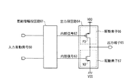
図1は、本発明の実施の形態に係る差動増幅器の回路構成図である。
図1に示す差動増幅器においては、入力差動信号40が差動増幅段回路41で増幅され、この増幅された内部信号42,43が出力段回路44へ出力され、それら信号42,43によって出力段回路44が動作されるようになっている。出力段回路44は、正側電源VDDと出力段回路44の出力端子45との間に第1の駆動素子46が接続され、また、負側電源VSSと出力端子45との間に第2の駆動素子47が接続されて構成されている。
Hereinafter, embodiments of the present invention will be described with reference to the drawings.
(Embodiment)
FIG. 1 is a circuit configuration diagram of a differential amplifier according to an embodiment of the present invention.
In the differential amplifier shown in FIG. 1, an input differential signal 40 is amplified by a differential amplifier stage circuit 41, and the amplified internal signals 42 and 43 are output to an output stage circuit 44. The output stage circuit 44 is operated. In the output stage circuit 44, the first drive element 46 is connected between the positive power supply VDD and the output terminal 45 of the output stage circuit 44, and the second drive power supply VSS is connected between the negative power supply VSS and the output terminal 45. A drive element 47 is connected.
第1の駆動素子46は、P型のMOSトランジスタP1とP2の並列接続で構成されており、P2の閾値電圧の絶対値はP1の閾値電圧の絶対値より大きい関係にある。またMOSトランジスタP1とP2のゲート端子にはともに内部信号42が供給されるようになっている。
第2の駆動素子47は、N型のMOSトランジスタN1とN2の並列接続で構成されており、N2の閾値電圧の絶対値はN1の閾値電圧の絶対値より大きい関係にある。またMOSトランジスタN1とN2のゲート端子にはともに内部信号43が供給されるようになっている。
The first drive element 46 is configured by parallel connection of P-type MOS transistors P1 and P2, and the absolute value of the threshold voltage of P2 is larger than the absolute value of the threshold voltage of P1. The internal signal 42 is supplied to the gate terminals of the MOS transistors P1 and P2.
The second drive element 47 is configured by parallel connection of N-type MOS transistors N1 and N2, and the absolute value of the threshold voltage of N2 is larger than the absolute value of the threshold voltage of N1. The internal signal 43 is supplied to the gate terminals of the MOS transistors N1 and N2.
また、駆動素子46と駆動素子47は、プッシュ・プル動作を行う。即ち、出力電流のソース時(出力端子から外部に電流を流しだす時)、駆動素子46は電流駆動力を上げ、駆動素子47は電流駆動力を下げ、両者の差分電流をソース電流として流出させる。また出力電流のシンク時(出力端子に外部から電流が流れ込む時)、駆動素子46は電流駆動力を下げ、駆動素子47は電流駆動力を上げ、両者の差分電流をシンク電流として流入させる。つまり2つの駆動素子46,47が相反する方向の動作(プッシュ・プル動作)を行うことで効率よく電流を流出・流入させる。 The drive element 46 and the drive element 47 perform a push-pull operation. That is, when the output current is sourced (when the current is started to flow from the output terminal to the outside), the driving element 46 increases the current driving force, the driving element 47 decreases the current driving force, and the difference current between the two flows out as the source current. . Further, when sinking the output current (when the current flows into the output terminal from the outside), the driving element 46 lowers the current driving force, the driving element 47 increases the current driving force, and flows the difference current between them as the sink current. That is, the two drive elements 46 and 47 perform an operation in the opposite direction (push / pull operation) to efficiently flow out and inflow current.
また、無信号出力状態では、内部信号42はMOSトランジスタP1をオンできるが、MOSトランジスタP2はオンできない程度の電位に設定され、P1がオンでP2がオフとなっている。同様に、内部信号43はMOSトランジスタN1をオンできるが、MOSトランジスタN2はオンできない程度の電位に設定され、N1がオンでN2がオフとなっている。
ここで、MOSトランジスタP1を流れる電流が全てN1を流れ、出力端子45からの入出力電流がない状態となっている。
また、MOSトランジスタP2はP1に比べて素子サイズが大きく、MOSトランジスタN2はN1に比べて素子サイズが大きい関係にある。
正極性の大信号を出力端子45から出力するために大電流をソースする場合は、内部信号42及び43が下降し、MOSトランジスタP1及びP2が強くオンになるが、P2がP1に対して大きくなっているため、駆動電流の大半がP2によって与えられるようになっている。
In the no-signal output state, the internal signal 42 is set to such a potential that the MOS transistor P1 can be turned on but the MOS transistor P2 cannot be turned on, and P1 is on and P2 is off. Similarly, the internal signal 43 is set to such a potential that the MOS transistor N1 can be turned on but the MOS transistor N2 cannot be turned on, and N1 is on and N2 is off.
Here, all the current flowing through the MOS transistor P1 flows through N1, and there is no input / output current from the output terminal 45.
The MOS transistor P2 has a larger element size than P1, and the MOS transistor N2 has a larger element size than N1.
When a large current is sourced in order to output a large positive signal from the output terminal 45, the internal signals 42 and 43 drop and the MOS transistors P1 and P2 are turned on strongly, but P2 is larger than P1. Therefore, most of the drive current is given by P2.
負極性の大信号を出力端子45から出力するために大電流をシンクする場合は、内部信号42及び43が上昇し、MOSトランジスタN1及びN2が強くオンになるが、N2がN1に対して大きくなっているため、駆動電流の大半がN2によって与えられるようになっている。
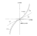
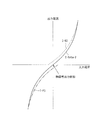
このような本実施の形態の差動増幅器における入力差動信号40の入力電圧と、出力端子45からの出力電流との関係を図2に示す。
曲線I−P1、I−P2、I−N1、I−N2は、それぞれMOSトランジスタP1、P2、N1、N2を流れる電流を表し、その総和が曲線I−total1で表す出力電流となる。
グラフ中央の「無信号出力状態」と指されているところでは、MOSトランジスタP1とN1がONとなっており、P2とN2はオフとなっているが、P1とN1を流れる電流が等しく、その差である出力電流I−total1はゼロとなっている。
When sinking a large current in order to output a large negative signal from the output terminal 45, the internal signals 42 and 43 rise and the MOS transistors N1 and N2 are strongly turned on, but N2 is larger than N1. Therefore, most of the drive current is supplied by N2.
FIG. 2 shows the relationship between the input voltage of the input differential signal 40 and the output current from the output terminal 45 in the differential amplifier of this embodiment.
Curves I-P1, I-P2, I-N1, and I-N2 represent currents that flow through the MOS transistors P1, P2, N1, and N2, respectively, and the sum thereof is an output current that is represented by the curve I-total1.
Where “no signal output state” is indicated in the center of the graph, the MOS transistors P1 and N1 are ON and P2 and N2 are OFF, but the currents flowing through P1 and N1 are equal, The output current I-total1 that is the difference is zero.
MOSトランジスタP1、N1は、小さ目のトランジスタで大き目のVONが与えられており、ゲート端子電圧の変化に対する電流変化の感度は低くなっている。正極性の大信号を出力するのは入力電圧が左側の方向に向かった場合でありP2の電流駆動力が支配的になる。また負極性の大信号を出力するのは入力電圧が右側の方向に向かった場合でありN2の電流駆動力が支配的になる。 The MOS transistors P1 and N1 are small transistors and are given a large VON, and the sensitivity of the current change to the change of the gate terminal voltage is low. A large positive signal is output when the input voltage is directed in the left direction, and the current driving force of P2 becomes dominant. A large negative signal is output when the input voltage is directed in the right direction, and the current driving force of N2 becomes dominant.
従来例と比較して本実施の形態の差動増幅器では、従来例のトランジスタP3と本実施の形態のトランジスタP2を同じ大きさにすることは可能であり、また従来例のトランジスタN3と本実施の形態のトランジスタN2を同じ大きさにすることは可能であるので、同等の駆動力を有することができる。
しかし、従来例の差動増幅器では無信号出力状態では、大きなトランジスタP3,N3で小さなVONが与えられる状態となっており、本実施の形態の差動増幅器では無信号出力状態では、小さなトランジスタP1,N1で大きなVONが与えられる状態となっており、前述の「背景技術」において原理を説明したとおり、本実施の形態の方が無信号出力状態の消費電流の個体間バラツキが小さくなる。
Compared to the conventional example, in the differential amplifier of this embodiment, the transistor P3 of the conventional example and the transistor P2 of this embodiment can be made the same size, and the transistor N3 of the conventional example and this embodiment Since the transistors N2 having the same configuration can be made the same size, they can have an equivalent driving force.
However, in the conventional differential amplifier, in the no-signal output state, a small VON is given by the large transistors P3 and N3. In the differential amplifier of the present embodiment, the small transistor P1 is in the no-signal output state. , N1 is a state in which a large VON is given, and as described in the above-mentioned “Background Art”, the variation in current consumption between individuals in the no-signal output state is smaller in this embodiment.
また、無信号出力時の消費電流の個体間バラツキが小さいので、電流が少なくなりすぎて発振等の不具合を発生するリスクが減るため、無信号出力時の消費電流を少なく設定することが可能になり、製造される多数個の個体の平均値としての無信号出力時の消費電流が少ない差動増幅器を製造することができるようになる。
以上、本発明を実施するための最良の形態について述べてきたが、本発明の差動増幅器を構成する素子、あるいは出力段回路を構成する駆動素子はMOSトランジスタで実現される場合のみならず、バイポーラトランジスタにより実現される物であっても良いし、MOSトランジスタとバイポーラトランジスタの混合により実現されるものであっても良い。
In addition, since there is little variation in the current consumption at the time of no signal output, the risk of causing problems such as oscillation due to too little current is reduced, so it is possible to set the current consumption at the time of no signal output low Accordingly, it is possible to manufacture a differential amplifier that consumes less current at the time of no-signal output as an average value of a large number of manufactured individuals.
As described above, the best mode for carrying out the present invention has been described. However, the element constituting the differential amplifier of the present invention or the drive element constituting the output stage circuit is not only realized by a MOS transistor, It may be realized by a bipolar transistor, or may be realized by mixing a MOS transistor and a bipolar transistor.
また、本発明における閾値電圧の異なる駆動素子は、拡散イオン濃度の差によって形成されるものであっても良いし、あるいは拡散されるイオン種の違い、複数種の配合されるイオン種の割合の違い、基盤のイオン濃度の違い、トランジスタのゲート端子長の違い、ゲート端子幅の違い、ゲート端子膜厚の違い等によって与えられるものであってもよい。
また、請求項4で述べられている素子サイズとは、素子の駆動能力のことを意図し、大きな素子とは大きな駆動力を有する素子ということである。MOSトランジスタの場合は、一例として電流通過方向のチャンネルの幅を「W」、電流通過方向のチャンネル長を「L」とするとW/Lという比率が大きい方が、駆動能力が大きくなるので素子サイズの大きな素子ということができる。
In addition, the drive elements having different threshold voltages in the present invention may be formed by the difference in the diffusion ion concentration, or the difference in the ion species to be diffused or the ratio of the ion species to be mixed in plural kinds. It may be given by a difference, a difference in ion concentration of a substrate, a difference in gate terminal length of a transistor, a difference in gate terminal width, a difference in gate terminal film thickness, or the like.
In addition, the element size described in claim 4 is intended for the drive capability of the element, and a large element is an element having a large drive force. In the case of a MOS transistor, for example, if the width of the channel in the current passing direction is “W” and the channel length in the current passing direction is “L”, the larger the ratio of W / L, the greater the driving capability. It can be said that the element is large.
従って、同じ「L」の素子同士である場合には「W」が大きな方の素子が素子サイズの大きな素子であり、同じ「W」の素子同士である場合には「L」が小さい方が大きな素子サイズとなる。バイポーラトランジスタの場合は、一例としてエミッタ面積に比例した駆動能力を有するときには、エミッタ面積の広い素子が大きな素子といえる。
次に、このような本実施の形態の差動増幅器を、より具体的に実現した実施例を説明する。
Therefore, in the case of the same “L” elements, the element having the larger “W” is the element having the larger element size, and in the case of the elements having the same “W”, the smaller “L”. Large element size. In the case of a bipolar transistor, for example, an element with a large emitter area can be said to be a large element when it has a driving capability proportional to the emitter area.
Next, an example in which the differential amplifier of the present embodiment is realized more specifically will be described.
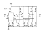
(第1の実施例)
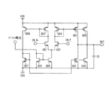
図3は、本発明の第1の実施例による差動増幅器の回路構成図であり、上記の実施の形態の原理に基き図7に示した従来例の差動増幅器を改良したものである。
図3に示す差動増幅器は、MOSトランジスタQ51〜Q62及びコンデンサC5を備えて構成されており、出力段回路には閾値電圧の低いP型のトランジスタQ62と閾値電圧の高いP型のトランジスタQ60が並列接続され、また閾値電圧の低いN型のトランジスタQ61と閾値電圧の高いN型のトランジスタQ59が並列接続されている。無信号出力時はQ62とQ61がオン、Q60とQ59がオフとなるようになされている。出力段回路の無信号出力時の消費電流はQ62とQ61で少なく設定され、大信号駆動時はQ60あるいはQ59で大駆動電流を得ることができる。
また、無信号出力時に出力段回路でオンとなっているQ62とQ61に適切なバイアス電位を設定するために、Q54とQ62は同じ閾値電圧の素子となっており、Q57とQ61も同じ閾値電圧の素子となっている。
(First embodiment)
FIG. 3 is a circuit configuration diagram of the differential amplifier according to the first example of the present invention, which is an improvement of the conventional differential amplifier shown in FIG. 7 based on the principle of the above embodiment.
The differential amplifier shown in FIG. 3 includes MOS transistors Q51 to Q62 and a capacitor C5. The output stage circuit includes a P-type transistor Q62 having a low threshold voltage and a P-type transistor Q60 having a high threshold voltage. An N-type transistor Q61 having a low threshold voltage and an N-type transistor Q59 having a high threshold voltage are connected in parallel. When no signal is output, Q62 and Q61 are turned on, and Q60 and Q59 are turned off. The current consumption during no signal output of the output stage circuit is set to be small at Q62 and Q61, and a large driving current can be obtained at Q60 or Q59 when driving a large signal.
Further, in order to set an appropriate bias potential to Q62 and Q61 that are turned on in the output stage circuit when no signal is output, Q54 and Q62 are elements having the same threshold voltage, and Q57 and Q61 are also the same threshold voltage. It becomes the element of.
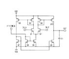
(第2の実施例)
図4は、本発明の第2の実施例による差動増幅器の回路構成図であり、上記の実施の形態の原理に基き図8に示した従来例の差動増幅器を改良したものである。
図4に示す差動増幅器は、MOSトランジスタQ63〜Q89、コンデンサC6〜C8、及び抵抗器R2を備えて構成されており、出力段回路には閾値電圧の低いP型のトランジスタQ88と閾値電圧の高いP型のトランジスタQ89が並列接続され、また閾値電圧の低いN型のトランジスタQ86と閾値電圧の高いN型のトランジスタQ87が並列接続されている。無信号出力時はQ88とQ86がオン、Q89とQ87がオフとなるようになされている。出力段回路の無信号出力時の消費電流はQ88とQ86で少なく設定され、大信号駆動時はQ89あるいはQ87で大駆動電流を得ることができる。
また、無信号出力時に出力段回路でオンとなっているQ88とQ86に適切なバイアス電位を設定するために、Q77、Q78、Q88は同じ閾値電圧の素子となっており、Q80、Q81、Q86も同じ閾値電圧の素子となっている。
(Second embodiment)
FIG. 4 is a circuit configuration diagram of a differential amplifier according to the second embodiment of the present invention, which is an improvement of the conventional differential amplifier shown in FIG. 8 based on the principle of the above embodiment.
The differential amplifier shown in FIG. 4 includes MOS transistors Q63 to Q89, capacitors C6 to C8, and a resistor R2. The output stage circuit includes a P-type transistor Q88 having a low threshold voltage and a threshold voltage. A high P-type transistor Q89 is connected in parallel, and an N-type transistor Q86 having a low threshold voltage and an N-type transistor Q87 having a high threshold voltage are connected in parallel. When no signal is output, Q88 and Q86 are turned on, and Q89 and Q87 are turned off. The current consumption during no-signal output of the output stage circuit is set to be small by Q88 and Q86, and when a large signal is driven, a large drive current can be obtained by Q89 or Q87.
Further, in order to set an appropriate bias potential to Q88 and Q86 that are turned on in the output stage circuit when no signal is output, Q77, Q78, and Q88 are elements having the same threshold voltage, and Q80, Q81, Q86. Are elements having the same threshold voltage.
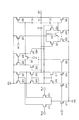
(第3の実施例)
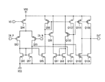
図5は、本発明の第3の実施例による差動増幅器の回路構成図であり、上記の実施の形態の原理に基き図9に示した従来例の差動増幅器を改良したものである。
図5に示す差動増幅器は、MOSトランジスタQ90〜Q106を備えて構成されており、出力段回路には閾値電圧の低いP型のトランジスタQ105と閾値電圧の高いP型のトランジスタQ106が並列接続され、また閾値電圧の低いN型のトランジスタQ103と閾値電圧の高いN型のトランジスタQ104が並列接続されており、無信号出力時はQ105とQ103がオン、Q106とQ104がオフとなるようになされている。出力段回路の無信号出力時の消費電流はQ105とQ103で少なく設定され、大信号駆動時はQ106あるいはQ104で大駆動電流を得ることができる。
また、無信号出力時に出力段回路でオンとなっているQ105とQ103に適切なバイアス電位を設定するために、Q100とQ105は同じ閾値電圧の素子となっている。
(Third embodiment)
FIG. 5 is a circuit diagram of a differential amplifier according to the third embodiment of the present invention, which is an improvement of the conventional differential amplifier shown in FIG. 9 based on the principle of the above-described embodiment.
The differential amplifier shown in FIG. 5 includes MOS transistors Q90 to Q106. A P-type transistor Q105 having a low threshold voltage and a P-type transistor Q106 having a high threshold voltage are connected in parallel to the output stage circuit. In addition, an N-type transistor Q103 having a low threshold voltage and an N-type transistor Q104 having a high threshold voltage are connected in parallel. When no signal is output, Q105 and Q103 are turned on, and Q106 and Q104 are turned off. Yes. The consumption current when no signal is output from the output stage circuit is set to be small by Q105 and Q103, and a large driving current can be obtained by Q106 or Q104 when driving a large signal.
Further, Q100 and Q105 are elements having the same threshold voltage in order to set an appropriate bias potential to Q105 and Q103 which are turned on in the output stage circuit when no signal is output.
(第4の実施例)
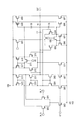
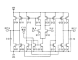
図6は、本発明の第4の実施例による差動増幅器の回路構成図であり、上記の第1の実施例の差動増幅器を改良したものである。
図6に示す差動増幅器は、MOSトランジスタQ107〜Q126とコンデンサC9,C10を備えて構成されており、出力段回路を2組有し、互いに相反する極性動作を行うことで全差動信号出力を得られるようになっている。このような差動増幅器と同等の回路は、全差動回路でも実現可能となっている。
OUT_Pを出力とする出力段回路には、閾値電圧の低いP型のトランジスタQ123と閾値電圧の高いP型のトランジスタQ124が並列接続され、また閾値電圧の低いN型のトランジスタQ125と閾値電圧の高いN型のトランジスタQ126が並列接続されている。
(Fourth embodiment)
FIG. 6 is a circuit diagram of a differential amplifier according to the fourth embodiment of the present invention, which is an improvement of the differential amplifier of the first embodiment.
The differential amplifier shown in FIG. 6 includes MOS transistors Q107 to Q126 and capacitors C9 and C10. The differential amplifier has two sets of output stage circuits, and performs fully opposite polarity operations by performing opposite polar operations. Can be obtained. A circuit equivalent to such a differential amplifier can also be realized by a fully differential circuit.
In the output stage circuit that outputs OUT_P, a P-type transistor Q123 having a low threshold voltage and a P-type transistor Q124 having a high threshold voltage are connected in parallel, and an N-type transistor Q125 having a low threshold voltage and a high threshold voltage are connected. N-type transistor Q126 is connected in parallel.
OUT_Nを出力とする他方の出力段回路には、閾値電圧の低いP型のトランジスタQ110と閾値電圧の高いP型のトランジスタQ109が並列接続され、また閾値電圧の低いN型のトランジスタQ108と閾値電圧の高いN型のトランジスタQ107が並列接続されている。
無信号出力時はQ123、Q125、Q110、Q108がオン、Q124、Q126、Q109、Q107がオフとなっている。出力段回路の無信号出力時の消費電流はQ123とQ125及びQ110とQ108で少なく設定され、大信号駆動時はQ124とQ107、あるいはQ126とQ109で大駆動電流を得ることができる。
In the other output stage circuit that outputs OUT_N, a P-type transistor Q110 having a low threshold voltage and a P-type transistor Q109 having a high threshold voltage are connected in parallel, and an N-type transistor Q108 having a low threshold voltage and a threshold voltage are connected. N-type transistor Q107 having a high value is connected in parallel.
When no signal is output, Q123, Q125, Q110, and Q108 are on, and Q124, Q126, Q109, and Q107 are off. The current consumption during no-signal output of the output stage circuit is set to be small by Q123 and Q125 and Q110 and Q108, and a large drive current can be obtained by Q124 and Q107 or Q126 and Q109 when driving a large signal.
また、無信号出力時に出力段回路でオンとなっているQ110、Q108、Q123、Q125に適切なバイアス電位を設定するために、Q110、Q113、Q119、Q120、Q122、Q123は同じ閾値電圧の素子となっており、Q108、Q114、Q121、Q125も同じ閾値電圧の素子となっている。
なお、本例の全差動回路の場合、出力の動作中点電圧を適正に維持するため、動作中点電圧を検出し、バイアス電流を制御するいわゆるコモンモードフィードバック回路も用いることが可能である。
In order to set an appropriate bias potential for Q110, Q108, Q123, and Q125 that are turned on in the output stage circuit when no signal is output, Q110, Q113, Q119, Q120, Q122, and Q123 are elements having the same threshold voltage. Q108, Q114, Q121, and Q125 are also elements having the same threshold voltage.
In the case of the fully differential circuit of this example, a so-called common mode feedback circuit that detects the operating midpoint voltage and controls the bias current can be used in order to properly maintain the operating midpoint voltage of the output. .
40 入力差動信号
41 差動増幅段回路
42,43 内部信号
44 出力段回路
45 出力端子
46 第1の駆動素子
47 第2の駆動素子
VDD 正側電源
VSS 負側電源
P1,P2 P型のMOSトランジスタ
N1,N2 N型のMOSトランジスタ
I−P1 MOSトランジスタP1を流れる電流を表す曲線
I−P2 MOSトランジスタP2を流れる電流を表す曲線
I−P3 MOSトランジスタP3を流れる電流を表す曲線
I−P4 MOSトランジスタP4を流れる電流を表す曲線
I−total1 MOSトランジスタP1〜P4の電流の総和を表す曲線
Q51,Q52、Q55,Q56,Q57,Q59,Q61,Q63,Q64,Q65,Q66,Q67,Q68,Q69,Q74,Q75,Q76,Q80,Q81,Q82,Q86,Q87,Q90,Q91,Q95,Q97,Q98,Q101,Q103,Q104,Q107,Q108,Q114,Q115,Q116,Q117,Q118,Q121,Q125,Q126 N型のMOSトランジスタ
Q53,Q54,Q58,Q60,Q62,Q70,Q71,Q72,Q73,Q77,Q78,Q79,Q83,Q84,Q85,Q88,Q89,Q92,Q93,Q94,Q96,Q99,Q100,Q102,Q105,Q106,Q109,Q110,Q113,Q119,Q120,Q122,Q123,Q124 P型のMOSトランジスタ
C5〜C10 コンデンサ
R2 抵抗器
40 Input Differential Signal 41 Differential Amplifier Stage Circuit 42, 43 Internal Signal 44 Output Stage Circuit 45 Output Terminal 46 First Drive Element 47 Second Drive Element VDD Positive Power Supply VSS Negative Power Supply P1, P2 P-type MOS Transistor N1, N2 N-type MOS transistor I-P1 Curve representing current flowing through MOS transistor P1 I-P2 Curve representing current flowing through MOS transistor P2 I-P3 Curve representing current flowing through MOS transistor P3 I-P4 MOS transistor Curve representing current flowing through P4 I-total1 Curve representing total current of MOS transistors P1 to P4 Q51, Q52, Q55, Q56, Q57, Q59, Q61, Q63, Q64, Q65, Q66, Q67, Q68, Q69, Q74, Q75, Q76, Q80, Q81, Q82, 86, Q87, Q90, Q91, Q95, Q97, Q98, Q101, Q103, Q104, Q107, Q108, Q114, Q115, Q116, Q117, Q118, Q121, Q125, Q126 N-type MOS transistors Q53, Q54, Q58, Q60, Q62, Q70, Q71, Q72, Q73, Q77, Q78, Q79, Q83, Q84, Q85, Q88, Q89, Q92, Q93, Q94, Q96, Q99, Q100, Q102, Q105, Q106, Q109, Q110, Q113, Q119, Q120, Q122, Q123, Q124 P-type MOS transistor C5 to C10 Capacitor R2 Resistor
Claims (4)
前記出力段回路は、
正側電源と当該出力段回路の出力端子との間に接続され、前記増幅信号に応じて電流駆動する第1の駆動回路と、
負側電源と当該出力段回路の出力端子との間に接続され、前記増幅信号に応じて電流駆動する第2の駆動回路とを備え、
前記第1及び第2の駆動回路の少なくとも1つは、各々閾値電圧が異なる2種類以上の能動素子が並列に接続されてなる
ことを特徴とする差動増幅器。 In a differential amplifier having a differential amplifier stage circuit that amplifies an input differential signal and an output stage circuit that operates according to an amplified signal output from the differential amplifier stage circuit,
The output stage circuit is
A first drive circuit connected between a positive-side power supply and an output terminal of the output stage circuit and current-driven in accordance with the amplified signal;
A second drive circuit connected between the negative power supply and the output terminal of the output stage circuit and driving the current according to the amplified signal;
At least one of the first and second drive circuits is formed by connecting in parallel two or more types of active elements each having a different threshold voltage.
ことを特徴とする請求項1に記載の差動増幅器。 The differential amplifier according to claim 1, wherein the first and second drive circuits perform a push-pull operation.
ことを特徴とする請求項1または請求項2に記載の差動増幅器。 Any of two or more types of active elements connected in parallel in at least one of the first and second drive circuits is in an off state when there is no signal output at the output terminal. The differential amplifier according to claim 1, wherein the differential amplifier is provided.
ことを特徴とする請求項1から3の何れか1項に記載の差動増幅器。 Two or more types of active elements connected in parallel in at least one of the first and second drive circuits are active elements having a large threshold voltage absolute value and an active element having a small threshold voltage absolute value. The differential amplifier according to any one of claims 1 to 3, wherein the differential amplifier is larger than an element size of the element.
Priority Applications (1)
| Application Number | Priority Date | Filing Date | Title |
|---|---|---|---|
| JP2003353709A JP4443889B2 (en) | 2003-10-14 | 2003-10-14 | Differential amplifier |
Applications Claiming Priority (1)
| Application Number | Priority Date | Filing Date | Title |
|---|---|---|---|
| JP2003353709A JP4443889B2 (en) | 2003-10-14 | 2003-10-14 | Differential amplifier |
Publications (2)
| Publication Number | Publication Date |
|---|---|
| JP2005123716A true JP2005123716A (en) | 2005-05-12 |
| JP4443889B2 JP4443889B2 (en) | 2010-03-31 |
Family
ID=34611917
Family Applications (1)
| Application Number | Title | Priority Date | Filing Date |
|---|---|---|---|
| JP2003353709A Expired - Fee Related JP4443889B2 (en) | 2003-10-14 | 2003-10-14 | Differential amplifier |
Country Status (1)
| Country | Link |
|---|---|
| JP (1) | JP4443889B2 (en) |
Cited By (4)
| Publication number | Priority date | Publication date | Assignee | Title |
|---|---|---|---|---|
| JP2007267016A (en) * | 2006-03-28 | 2007-10-11 | Ricoh Co Ltd | Operational amplifier |
| JP2010258902A (en) * | 2009-04-27 | 2010-11-11 | Renesas Electronics Corp | Output circuit using analog amplifier circuit |
| JP2016516374A (en) * | 2013-04-11 | 2016-06-02 | スナップトラック・インコーポレーテッド | Output stage of class AB amplifier |
| JP6625272B1 (en) * | 2018-11-29 | 2019-12-25 | 三菱電機株式会社 | Active circulator |
-
2003
- 2003-10-14 JP JP2003353709A patent/JP4443889B2/en not_active Expired - Fee Related
Cited By (7)
| Publication number | Priority date | Publication date | Assignee | Title |
|---|---|---|---|---|
| JP2007267016A (en) * | 2006-03-28 | 2007-10-11 | Ricoh Co Ltd | Operational amplifier |
| JP2010258902A (en) * | 2009-04-27 | 2010-11-11 | Renesas Electronics Corp | Output circuit using analog amplifier circuit |
| CN101931373A (en) * | 2009-04-27 | 2010-12-29 | 瑞萨电子株式会社 | Output circuit using an analog amplifier |
| CN101931373B (en) * | 2009-04-27 | 2014-05-14 | 瑞萨电子株式会社 | Output circuit using analog amplifier |
| JP2016516374A (en) * | 2013-04-11 | 2016-06-02 | スナップトラック・インコーポレーテッド | Output stage of class AB amplifier |
| JP6625272B1 (en) * | 2018-11-29 | 2019-12-25 | 三菱電機株式会社 | Active circulator |
| WO2020110252A1 (en) * | 2018-11-29 | 2020-06-04 | 三菱電機株式会社 | Active circulator |
Also Published As
| Publication number | Publication date |
|---|---|
| JP4443889B2 (en) | 2010-03-31 |
Similar Documents
| Publication | Publication Date | Title |
|---|---|---|
| US7956597B2 (en) | Reference buffer circuits for providing reference voltages | |
| US7737790B1 (en) | Cascode amplifier and method for controlling current of cascode amplifier | |
| US7719345B2 (en) | Reference buffer circuits | |
| CN102158216A (en) | Receiving circuit | |
| CN101505141A (en) | Reference buffer | |
| JP2005354266A (en) | Voltage comparator circuit | |
| JP2008288900A (en) | Differential amplifier | |
| EP3826176B1 (en) | High-linearity input buffer | |
| US7629834B2 (en) | Limiter circuit | |
| CN101521489A (en) | Amplifier and class AB amplifier | |
| US8130034B2 (en) | Rail-to-rail amplifier | |
| JP4443889B2 (en) | Differential amplifier | |
| US7956690B2 (en) | Operational amplification circuit | |
| JP2013005447A (en) | Method and apparatus for biasing rail-to-rail dmos amplifier output stage | |
| US7816989B2 (en) | Differential amplifier | |
| CN102447443A (en) | Differential amplifier circuit | |
| US11848649B2 (en) | Low power VB class AB amplifier with local common mode feedback | |
| JP3936952B2 (en) | AB class CMOS output circuit | |
| JP2015159462A (en) | Voltage follower circuit | |
| JP4725472B2 (en) | Subtraction circuit and operational amplifier | |
| JP2012156826A (en) | Comparator | |
| JP5450226B2 (en) | Duty ratio automatic adjustment comparator circuit | |
| US7579911B2 (en) | Semiconductor circuit | |
| TWI888005B (en) | Voltage follower | |
| JP5203809B2 (en) | Current mirror circuit |
Legal Events
| Date | Code | Title | Description |
|---|---|---|---|
| A621 | Written request for application examination |
Free format text: JAPANESE INTERMEDIATE CODE: A621 Effective date: 20060712 |
|
| A521 | Written amendment |
Free format text: JAPANESE INTERMEDIATE CODE: A821 Effective date: 20070402 |
|
| A711 | Notification of change in applicant |
Free format text: JAPANESE INTERMEDIATE CODE: A712 Effective date: 20070402 |
|
| A977 | Report on retrieval |
Free format text: JAPANESE INTERMEDIATE CODE: A971007 Effective date: 20090113 |
|
| A131 | Notification of reasons for refusal |
Free format text: JAPANESE INTERMEDIATE CODE: A131 Effective date: 20090120 |
|
| A521 | Written amendment |
Free format text: JAPANESE INTERMEDIATE CODE: A523 Effective date: 20090316 |
|
| A131 | Notification of reasons for refusal |
Free format text: JAPANESE INTERMEDIATE CODE: A131 Effective date: 20090721 |
|
| A521 | Written amendment |
Free format text: JAPANESE INTERMEDIATE CODE: A523 Effective date: 20090806 |
|
| TRDD | Decision of grant or rejection written | ||
| A01 | Written decision to grant a patent or to grant a registration (utility model) |
Free format text: JAPANESE INTERMEDIATE CODE: A01 Effective date: 20100105 |
|
| A01 | Written decision to grant a patent or to grant a registration (utility model) |
Free format text: JAPANESE INTERMEDIATE CODE: A01 |
|
| A61 | First payment of annual fees (during grant procedure) |
Free format text: JAPANESE INTERMEDIATE CODE: A61 Effective date: 20100113 |
|
| R150 | Certificate of patent or registration of utility model |
Ref document number: 4443889 Country of ref document: JP Free format text: JAPANESE INTERMEDIATE CODE: R150 Free format text: JAPANESE INTERMEDIATE CODE: R150 |
|
| FPAY | Renewal fee payment (event date is renewal date of database) |
Free format text: PAYMENT UNTIL: 20130122 Year of fee payment: 3 |
|
| FPAY | Renewal fee payment (event date is renewal date of database) |
Free format text: PAYMENT UNTIL: 20140122 Year of fee payment: 4 |
|
| LAPS | Cancellation because of no payment of annual fees |