JP2005123740A - High frequency switch module - Google Patents
High frequency switch module Download PDFInfo
- Publication number
- JP2005123740A JP2005123740A JP2003354151A JP2003354151A JP2005123740A JP 2005123740 A JP2005123740 A JP 2005123740A JP 2003354151 A JP2003354151 A JP 2003354151A JP 2003354151 A JP2003354151 A JP 2003354151A JP 2005123740 A JP2005123740 A JP 2005123740A
- Authority
- JP
- Japan
- Prior art keywords
- switch module
- frequency switch
- module according
- gallium arsenide
- circuit
- Prior art date
- Legal status (The legal status is an assumption and is not a legal conclusion. Google has not performed a legal analysis and makes no representation as to the accuracy of the status listed.)
- Granted
Links
- JBRZTFJDHDCESZ-UHFFFAOYSA-N AsGa Chemical compound [As]#[Ga] JBRZTFJDHDCESZ-UHFFFAOYSA-N 0.000 claims abstract description 84
- 230000005540 biological transmission Effects 0.000 claims abstract description 43
- 229910001218 Gallium arsenide Inorganic materials 0.000 claims description 80
- 239000003990 capacitor Substances 0.000 claims description 33
- 238000009966 trimming Methods 0.000 claims description 11
- 230000005611 electricity Effects 0.000 claims description 9
- 230000003068 static effect Effects 0.000 claims description 9
- 239000004020 conductor Substances 0.000 claims description 3
- 238000013459 approach Methods 0.000 abstract description 2
- 238000010586 diagram Methods 0.000 description 23
- 238000004891 communication Methods 0.000 description 10
- 238000003780 insertion Methods 0.000 description 7
- 230000037431 insertion Effects 0.000 description 7
- 238000000034 method Methods 0.000 description 7
- 239000000758 substrate Substances 0.000 description 3
- 239000000919 ceramic Substances 0.000 description 2
- 230000000694 effects Effects 0.000 description 2
- 230000009467 reduction Effects 0.000 description 2
- 238000010897 surface acoustic wave method Methods 0.000 description 2
- 230000001413 cellular effect Effects 0.000 description 1
- 230000000593 degrading effect Effects 0.000 description 1
- 230000005669 field effect Effects 0.000 description 1
- 238000004519 manufacturing process Methods 0.000 description 1
- 238000010295 mobile communication Methods 0.000 description 1
- 230000001902 propagating effect Effects 0.000 description 1
- 230000009466 transformation Effects 0.000 description 1
Images





Classifications
-
- H—ELECTRICITY
- H04—ELECTRIC COMMUNICATION TECHNIQUE
- H04B—TRANSMISSION
- H04B1/00—Details of transmission systems, not covered by a single one of groups H04B3/00 - H04B13/00; Details of transmission systems not characterised by the medium used for transmission
- H04B1/38—Transceivers, i.e. devices in which transmitter and receiver form a structural unit and in which at least one part is used for functions of transmitting and receiving
- H04B1/40—Circuits
- H04B1/44—Transmit/receive switching
- H04B1/48—Transmit/receive switching in circuits for connecting transmitter and receiver to a common transmission path, e.g. by energy of transmitter
-
- H—ELECTRICITY
- H04—ELECTRIC COMMUNICATION TECHNIQUE
- H04B—TRANSMISSION
- H04B1/00—Details of transmission systems, not covered by a single one of groups H04B3/00 - H04B13/00; Details of transmission systems not characterised by the medium used for transmission
- H04B1/005—Details of transmission systems, not covered by a single one of groups H04B3/00 - H04B13/00; Details of transmission systems not characterised by the medium used for transmission adapting radio receivers, transmitters andtransceivers for operation on two or more bands, i.e. frequency ranges
- H04B1/0053—Details of transmission systems, not covered by a single one of groups H04B3/00 - H04B13/00; Details of transmission systems not characterised by the medium used for transmission adapting radio receivers, transmitters andtransceivers for operation on two or more bands, i.e. frequency ranges with common antenna for more than one band
- H04B1/006—Details of transmission systems, not covered by a single one of groups H04B3/00 - H04B13/00; Details of transmission systems not characterised by the medium used for transmission adapting radio receivers, transmitters andtransceivers for operation on two or more bands, i.e. frequency ranges with common antenna for more than one band using switches for selecting the desired band
Landscapes
- Engineering & Computer Science (AREA)
- Computer Networks & Wireless Communication (AREA)
- Signal Processing (AREA)
- Transceivers (AREA)
Abstract
Description
本発明は、高周波スイッチモジュールに関し、特に複数の通信システムのフロントエンドモジュールとして使用される高周波スイッチモジュールに関する。 The present invention relates to a high-frequency switch module, and more particularly to a high-frequency switch module used as a front-end module for a plurality of communication systems.
近年、例えば携帯電話機では、機能やサービスの向上が図られている。その一環として、複数の通信システムで使用が可能な携帯電話機が提供されている。 In recent years, for example, functions and services have been improved in mobile phones. As part of this, mobile phones that can be used in a plurality of communication systems have been provided.
このような携帯電話機に代表される通信機器では、異なった周波数帯域を使用する必要がある。例えば最近開発されたトリプルバンドの携帯電話機は、GSM(Global System for Mobile Communications)方式やDCS(Digital Communications System)方式やPCS(Personal Communications Service)方式等の3つの送受信系を取り扱うことができるように構成されている。 A communication device represented by such a mobile phone needs to use different frequency bands. For example, a recently developed triple-band mobile phone can handle three transmission / reception systems such as GSM (Global System for Mobile Communications), DCS (Digital Communications System), and PCS (Personal Communications Service). It is configured.
但し、GSM方式とDCS方式とPCS方式とでは、それぞれ使用する周波数帯域が異なる。このため、上記のように複数の方式を使用する携帯電話には、使用する周波数帯域を切り替えるためのスイッチが組み込まれている。 However, the GSM method, DCS method, and PCS method use different frequency bands. For this reason, a switch for switching a frequency band to be used is incorporated in a mobile phone using a plurality of systems as described above.
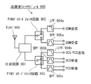
使用する周波数帯域を切り替えるスイッチとしては、例えば以下の特許文献1及び2に開示されるような、分波回路とPINダイオードスイッチ回路とを有して構成された高周波スイッチモジュール等が存在する。このような高周波スイッチモジュール900の一例を図1に示す。
As a switch for switching the frequency band to be used, there is a high-frequency switch module configured by including a branching circuit and a PIN diode switch circuit as disclosed in, for example,
図1に示すように、高周波スイッチモジュール900は、アンテナ909に接続された分波回路901と、分波回路901に接続された2つのPINダイオードスイッチ回路902,903と、PINダイオードスイッチ回路902に接続されたローパスフィルタ(Low-Pass Filter:以下、LPFと略す)904a及びバンドパスフィルタ(Band-Pass Filter:以下、BPFと略す)905aと、PINダイオードスイッチ回路903に接続されたLPF904b,BPF905b及びBPF905cとを有する。
As shown in FIG. 1, the high
分波回路901はアンテナ909から入力された高周波信号を分波し、これをPINダイオードスイッチ回路902又は903に入力すると共に、PINダイオードスイッチ回路902又は903から入力された高周波信号をアンテナへ出力する。PINダイオードスイッチ回路902は、2種類の周波数を切り替えるために、高周波信号の入出力先をLPF904a又はBPF905aに切り替える。また、PINダイオードスイッチ回路903は、3種類の周波数を切り替えるために、高周波信号の入出力先をLPF904b,BPF905b又はBPF905cに切り替える。以上のような構成により、合計3つの送受信系を取り扱うことが可能となる。
The demultiplexing circuit 901 demultiplexes the high-frequency signal input from the antenna 909, inputs this to the PIN diode switch circuit 902 or 903, and outputs the high-frequency signal input from the PIN diode switch circuit 902 or 903 to the antenna. . The PIN diode switch circuit 902 switches the input / output destination of the high-frequency signal to the
しかしながら、上記のような高周波スイッチモジュールでは、それぞれの通信方式を切り替えるために分波回路等を必要としているため、部品点数が多く、小型化及び低背化が困難であるという問題が存在する。 However, the above-described high-frequency switch module requires a branching circuit or the like to switch each communication method, and thus has a problem that the number of parts is large and it is difficult to reduce the size and the height.
また、分波回路とPINダイオードスイッチ回路とを有して構成されている高周波スイッチモジュールは、低挿入損失を実現するために、一般的にPINダイオードに十分な電流を流す必要がある。このため、このような回路構成では消費電力が増加してしまうという問題も存在する。特に携帯電話機等のような電池駆動を必要とする電子機器では、上記の問題により電池寿命が早められるため、これら電子機器の駆動時間を減少させるという問題を誘発する。 In addition, a high-frequency switch module configured to include a branching circuit and a PIN diode switch circuit generally requires a sufficient current to flow through the PIN diode in order to realize low insertion loss. For this reason, such a circuit configuration also has a problem that power consumption increases. In particular, in an electronic device such as a cellular phone that requires battery driving, the battery life is shortened due to the above-described problem, which causes a problem of reducing the driving time of these electronic devices.
このような問題を解決する技術として、例えば特許文献3に開示されるように、PINダイオードスイッチ回路と比較して省電力である砒化ガリウム(GaAs)スイッチを用いる構成が存在する。
しかしながら、GaAsスイッチは通過帯域外の減衰量が小さいため、これを用いて複数の周波数帯域を切り替える高周波スイッチモジュールを構成した場合、選択状態にある送受信系が他の送受信系から影響を受けてしまう問題が存在する。 However, since the GaAs switch has a small attenuation outside the passband, when a high-frequency switch module for switching a plurality of frequency bands using this is configured, the selected transmission / reception system is affected by other transmission / reception systems. There is a problem.
そこで本発明は、上記の問題を鑑み、消費電力が少なく且つ小型化及び低背化が可能な高周波スイッチモジュールであって、通過帯域外の減衰量を確保し、良好な特性を得られる高周波スイッチモジュールを提供することを目的とする。 In view of the above problems, the present invention is a high-frequency switch module that consumes less power and can be reduced in size and height, and can secure attenuation characteristics outside the passband and obtain good characteristics. The purpose is to provide modules.
かかる目的を達成するために、本発明は、請求項1記載のように、送信系毎に設けられたローパスフィルタと、該ローパスフィルタの何れかに接続を切り替える砒化ガリウムスイッチとを有する高周波スイッチモジュールであって、前記ローパスフィルタは、並列に接続された第1のインダクタ及びコンデンサと、当該ローパスフィルタの入出力側にそれぞれ設けられた第2及び第3のインダクタとを有し、前記第2及び第3のインダクタのインダクタンスが前記第1のインダクタのインダクタンスよりも大きいように構成される。消費電流が比較的少ない素子である砒化ガリウム(GaAs)を用いて作製されたGaAsスイッチを使用することにより、PINダイオードスイッチを使用した場合と比較して大幅に消費電流を低減することが可能となる。また、GaAsスイッチを使用することで、消費電流の低減を目的とした回路素子を必要としないため、高周波スイッチモジュールの小型化及び低背化も可能となる。更に、送信系にローパスフィルタ(LPF)を設け、このローパスフィルタの入出力端に第2及び第3のインダクタンスを付加することで、所望する周波数帯域外の減衰量を確保することができ、良好な製品特性を実現することができる。この際、入出力端に設けた第2及び第3のインダクタのインダクタンスが、これらの間に設けられた第1のインダクタのインダクタンスよりも大きくなるように構成することで、ローパスフィルタの周波数帯域外での入力インピーダンスが無限大に近づくため、更に良好な製品特性を実現することができる。 In order to achieve this object, the present invention provides a high frequency switch module having a low pass filter provided for each transmission system and a gallium arsenide switch that switches connection to any of the low pass filters. The low-pass filter includes a first inductor and a capacitor connected in parallel, and second and third inductors provided on the input and output sides of the low-pass filter, respectively. The inductance of the third inductor is configured to be larger than the inductance of the first inductor. By using a GaAs switch manufactured using gallium arsenide (GaAs), which is an element that consumes relatively little current, it is possible to significantly reduce current consumption compared to using a PIN diode switch. Become. In addition, the use of the GaAs switch eliminates the need for a circuit element intended to reduce current consumption, thereby enabling the high-frequency switch module to be reduced in size and height. Furthermore, by providing a low-pass filter (LPF) in the transmission system and adding the second and third inductances to the input and output ends of this low-pass filter, it is possible to secure an attenuation amount outside the desired frequency band, which is good Product characteristics can be realized. At this time, the second and third inductors provided at the input / output terminals are configured so that the inductance of the first inductor provided therebetween is larger than the frequency band of the low-pass filter. Since the input impedance at the end approaches infinity, even better product characteristics can be realized.
請求項1記載の前記高周波スイッチモジュールは、例えば請求項2記載のように、受信系毎に設けられたバンドパスフィルタを有し、前記砒化ガリウムスイッチが前記ローパスフィルタ及び前記バンドパスフィルタの何れかに接続を切り替えるように構成されても良い。
The high-frequency switch module according to
請求項2記載の前記高周波スイッチモジュールは、請求項3記載のように、前記バンドパスフィルタと前記砒化ガリウムスイッチとを接続する配線上にインピーダンス調整回路を有することが好ましい。バンドパスフィルタのインピーダンスを調整することで、各バンドパスフィルタの挿入損失がばらつくことを防止でき、製品としての特性のばらつきを防止することができる。 According to a second aspect of the present invention, it is preferable that the high-frequency switch module has an impedance adjustment circuit on a wiring connecting the band-pass filter and the gallium arsenide switch. By adjusting the impedance of the band-pass filter, it is possible to prevent variation in insertion loss of each band-pass filter and to prevent variation in characteristics as a product.
また、請求項1記載の前記高周波スイッチモジュールは、請求項4記載のように、受信系毎に設けられたバンドパスフィルタと、前記砒化ガリウムスイッチから入力された高周波信号を分波する分波回路とを有し、前記バンドパスフィルタの少なくとも2つが前記分波回路を介して前記砒化ガリウムスイッチにおける同一の端子に接続されていることが好ましい。GaAsスイッチの端子を2つ以上のバンドパスフィルタで共用することで、より小型のGaAsスイッチを使用することが可能となるため、更に製品を小型化することができる。
The high-frequency switch module according to
請求項4記載の前記高周波スイッチモジュールは、請求項5記載のように、前記分波回路に接続されていない前記バンドパスフィルタと前記砒化ガリウムとを接続する配線上にインピーダンス調整回路を有することが好ましい。分波回路を介さないバンドパスフィルタのインピーダンスを調整することで、各バンドパスフィルタの挿入損失がばらつくことを防止でき、製品としての特性のばらつきを防止することができる。
The high-frequency switch module according to claim 4 has an impedance adjustment circuit on a wiring connecting the band-pass filter not connected to the branching circuit and the gallium arsenide as described in
また、請求項1記載の前記高周波スイッチモジュールは、請求項6記載のように、受信系毎に設けられたバンドパスフィルタを有し、前記バンドパスフィルタと前記砒化ガリウムスイッチとを接続する配線の少なくとも2つは共通化された後に前記砒化ガリウムスイッチにおける同一の端子に接続され、また、共通化される前記配線の少なくとも1つにインピーダンス調整回路を有することが好ましい。GaAsスイッチの端子を2つ以上のバンドパスフィルタで共用することで、より小型のGaAsスイッチを使用することが可能となるため、更に製品を小型化することができる。また、これを分波回路を用いずに構成することで、更なる製品の小型化を実現することができる。
The high-frequency switch module according to
また、請求項1から6の何れか1項に記載の前記砒化ガリウムスイッチは、請求項7記載のように、複数のトランジスタと、外部から入力された切替信号を前記トランジスタのオン/オフを制御するための制御電圧にデコードするデコーダとを有することが好ましい。これにより、デコーダを外部回路として設ける必要がないため、製品の汎用性を向上させることができる。
The gallium arsenide switch according to any one of
また、請求項1から6の何れか1項に記載の前記高周波スイッチモジュールは、請求項8記載のように、前記砒化ガリウムスイッチをアンテナを介して印加された静電気から保護するための保護回路を有することが好ましい。GaAsスイッチは一般的に静電気に対して弱い。そこで、保護回路を用いてGaAsスイッチを静電気から保護することで、製品の耐久性及び寿命を向上させることができる。
The high-frequency switch module according to any one of
請求項8記載の前記保護回路は、例えば請求項9記載のように、ハイパスフィルタであってもよい。これにより、簡素な構成でGaAsスイッチを静電気から保護することが可能となる。 The protection circuit according to claim 8 may be a high-pass filter as described in claim 9, for example. This makes it possible to protect the GaAs switch from static electricity with a simple configuration.
また、請求項1から6の何れか1項に記載の前記高周波スイッチモジュールは、例えば請求項10記載のように、前記送信系が2つであり、前記ローパスフィルタが全ての前記送信系に設けられているように構成されても良い。
Further, in the high-frequency switch module according to any one of
また、請求項2、4又は6記載の前記高周波スイッチモジュールは、例えば請求項11記載のように、前記受信系が3つであり、前記バンドパスフィルタが少なくとも2つの前記受信系に設けられているように構成されても良い。
Further, in the high frequency switch module according to
また、請求項3、5又は6記載の前記高周波スイッチモジュールは、請求項12記載のように、前記インピーダンス調整回路がインダクタ,コンデンサ又は伝送線路を含み、前記インダクタ,前記コンデンサ又は前記伝送線路がインダクタンス又は静電容量をトリミングにより調整可能な導体パターンで形成されていることが好ましい。トリミングにより調整可能な導体パターンを用いることで、作製後の微調整が可能となるため、製品の特性を向上させることができると共に、その歩留りを向上させることもできる。
Further, in the high-frequency switch module according to
また、請求項1から6の何れか1項に記載の前記高周波スイッチモジュールは、請求項13記載のように、前記ローパスフィルタと前記砒化ガリウムスイッチとが同一パッケージ内に実装されていることが好ましい。1パッケージとして作製することで、使い勝手の良い高周波スイッチモジュールを実現することができる。
Further, in the high-frequency switch module according to any one of
本発明によれば、消費電力が少なく且つ小型化及び低背化が可能な高周波スイッチモジュールであって、通過帯域外の減衰量を確保し、良好な特性を得られる高周波スイッチモジュールを実現することができる。 According to the present invention, a high-frequency switch module that consumes less power and can be reduced in size and height and that can secure attenuation outside the passband and achieve good characteristics can be realized. Can do.
以下、本発明を実施するための最良の形態を図面と共に詳細に説明する。 Hereinafter, the best mode for carrying out the present invention will be described in detail with reference to the drawings.
まず、本発明による実施例1について以下に詳細に説明する。 First, Example 1 according to the present invention will be described in detail below.
本実施例では、消費電流が比較的少ない素子である砒化ガリウム(GaAs)を用いて作製されたスイッチ(以下、GaAsスイッチという)を使用する。これにより、PINダイオードスイッチを使用した場合と比較して大幅に消費電流を低減することが可能となる。また、GaAsスイッチを使用することで、消費電流の低減を目的とした回路素子を必要としないため、高周波スイッチモジュールの小型化及び低背化も可能となる。更に本実施例では、送信系にローパスフィルタ(LPF)を設け、このLPFの入出力端にインダクタンスを付加する。この際、入出力端に設けたインダクタンスが、これらの間に設けられたインダクタンスよりも大きくなるように構成することで、LPFの周波数帯域外での入力インピーダンスを無限大に近づける。これにより、周波数帯域外での減衰量を確保することが可能となり、良好な製品特性を実現することができる。 In this embodiment, a switch (hereinafter referred to as a GaAs switch) manufactured using gallium arsenide (GaAs), which is an element with relatively low current consumption, is used. As a result, the current consumption can be greatly reduced as compared with the case where a PIN diode switch is used. In addition, the use of the GaAs switch eliminates the need for a circuit element intended to reduce current consumption, thereby enabling the high-frequency switch module to be reduced in size and height. Furthermore, in this embodiment, a low pass filter (LPF) is provided in the transmission system, and inductance is added to the input / output end of this LPF. At this time, the input impedance outside the frequency band of the LPF is brought to infinity by configuring the inductance provided at the input / output end to be larger than the inductance provided between them. As a result, it is possible to secure an attenuation amount outside the frequency band, and to realize good product characteristics.
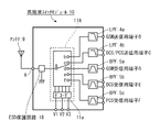
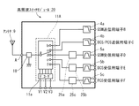
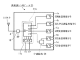
以下、本実施例による高周波スイッチモジュールを図面を用いて詳細に説明する。図2は、本実施例による高周波スイッチモジュール10の構成を示す回路図である。図2に示すように、高周波スイッチモジュール10は、GaAsスイッチ11Aと、GSM送信系のLPF4aと、DCS/PCS送信系のLPF4bと、GSM受信系のBPF5aと、DCS受信系のBPF5bと、PCS受信系のBPF5cとを有して構成されている。
Hereinafter, the high-frequency switch module according to the present embodiment will be described in detail with reference to the drawings. FIG. 2 is a circuit diagram showing the configuration of the high-
GaAsスイッチ11Aは、1端子(a)対多端子(本実施例ではb〜fの5端子)の切替スイッチであり、外部から入力された切替信号に基づいて端子aと端子b〜fの何れかとを接続するように動作する。尚、GaAsスイッチ11Aには、外部からの切替信号をデコードするデコーダ11aが組み込まれている。デコーダ11aには、3つの制御端子V1,V2及びV3が設けられており、これらの制御端子V1〜V3に3ビットの切替信号が入力される。デコーダ11aは、入力された切替信号を、端子aの接続先を切り替えるための制御電圧に変換する。すなわち、デコーダ11aは、3つの制御端子V1〜V3に入力された切替信号における各ビットの電圧レベル(High/Low)に基づいて、端子aの接続先を切り替える。
The
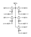
ここで、本実施例で使用するGaAsスイッチ11Aの回路構成を図3に示す。尚、図3の構成では、説明の簡略化のため、デコーダ11aの構成を省略する。図3に示すように、GaAsスイッチ11Aは、5つの電界効果型トランジスタ(Field Effect Transistor:以下、FETという)Q1〜Q5と、これらのゲート電極にそれぞれ設けられた抵抗R1〜5とを有して構成される。FETQ1〜Q5のソース電極及びドレイン電極の一方は、共通化された後、端子aに接続される。FETQ1〜Q5のドレイン電極及びソース電極の他方には、それぞれ端子b〜fが1対1で接続される。また、抵抗R1〜R5において、FETQ1〜Q5のゲート電極に接続された端と反対側の端は、それぞれコントロール端子I,II,III,IV及びVに接続される。尚、コントロール端子I,II,III,IV及びVには、デコーダ11aでデコードされた切替電圧が印加される。従って、デコードされた切替電圧に従って何れかのFET(Q1〜Q5の何れか)が導通することで、このFETに対応する端子(b〜fの何れか)と端子aとの1対1の接続が成される。ここで、デコーダ11aの制御端子V1〜V3の電圧レベルとコントロール端子I〜Vの電圧レベルとのデコード対応、すなわち送受信切替ロジックの一例を表1に示す。
Here, FIG. 3 shows a circuit configuration of the
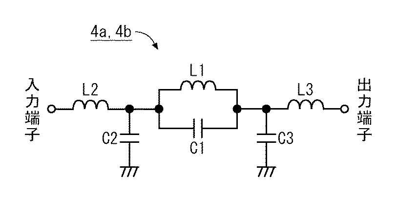
表1に示すようなロジックに従ってFETQ1〜Q5のオン/オフを切り替えることで、端子aと端子b〜fの何れかとの1対1の対応を得ることができる。すなわち、GaAsスイッチ11Aが、LPF4a,4b及びBPF5a,5b,5cの何れかに接続を切り替えることができる。
By switching on / off the FETs Q1 to Q5 according to the logic shown in Table 1, a one-to-one correspondence between the terminal a and any of the terminals b to f can be obtained. That is, the
図2に戻って説明する。GaAsスイッチ11Aにおける端子aには、GaAsスイッチ11Aを静電気等から保護するためのESD(Electro-Static Discharge)保護回路18が接続される。尚、ESD保護回路18は外部端子であるアンテナ端子Aを介してアンテナ9に接続される。
Returning to FIG. An ESD (Electro-Static Discharge)
ESD保護回路18は、例えばハイパスフィルタ(High-Pass Filter:HPF)で構成されており、アンテナ9から印加された静電気がGaAsスイッチ11Aに入力することを防止する。GaAsスイッチ11Aは一般的に静電気に弱いため、アンテナ9との間にESD保護回路18を設けることで効果的にGaAsスイッチ11Aを保護することが可能となる。図4(a)及び(b)に、HPFで構成されたESD保護回路18の構成例を示す。
The
図4(a)は、ESD保護回路18をT型のHPFで構成した場合の第1の構成例を示す回路図である。図4(a)に示すように、この場合のESD保護回路18は、入力端子と出力端子との間に直列に接続された2つのコンデンサC181及びC182を有する。各コンデンサC181,C182を接続する配線は分岐され、直列に接続されたインダクタL181及びコンデンサC183を介して接地される。
FIG. 4A is a circuit diagram illustrating a first configuration example when the
また、図4(b)は、ESD保護回路18をπ型のHPFで構成した場合の第2の構成例を示す回路図である。図4(b)に示すように、この場合のESD保護回路18は、入力端子と接続端子との間に並列に接続されたインダクタL185及びコンデンサC185を有する。インダクタL185とコンデンサC185とを接続する一方の配線と入力端子との間は分岐され、インダクタL186を介して接地される。同様に、インダクタL185とコンデンサC185とを接続する他方の配線と出力端子との間は分岐され、インダクタL187を介して接地される。
FIG. 4B is a circuit diagram showing a second configuration example when the
以上のような回路構成を有するESD保護回路18をアンテナ9とGaAsスイッチ11Aとの間に設けることで、静電気がアンテナ9を介してGaAsスイッチ11Aに印加されることを防止でき、これが破損することを回避できる。
By providing the
図2に戻って説明する。GaAsスイッチ11Aにおける端子b〜fには、各通信システムにおけるそれぞれの周波数帯域を通過させるためのLPF4a及び4b並びにBPF5a,5b及び5cが接続される。すなわち、送信系毎に設けられたLPF(4a,4b)と受信系毎に設けられたBPF(5a,5b,5c)とがそれぞれ接続されている。具体的には、端子bとGSM送信用端子Bとの間及び端子cとDCS/PCS送信用端子Cとの間にLPF4a及び4bがそれぞれ接続され、端子dとGSM受信用端子Dとの間,端子eとDCS受信用端子Eとの間及び端子fとPCS受信用端子Fとの間にBPF5a,5b及び5cがそれぞれ接続される。但し、BPF5a,5b及び5cを弾性表面波(Surface Acoustic Wave:SAW)フィルタで構成しても良い。また、GSM送信用端子BとDCS/PCS送信用端子CとGSM受信用端子DとDCS受信用端子EとPCS受信用端子Fとは外部端子であり、それぞれの通信システムに適合した回路が接続される。
Returning to FIG. LPFs 4a and 4b and BPFs 5a, 5b and 5c for passing the respective frequency bands in each communication system are connected to terminals b to f in the
GSM送信系及びDCS/PCS送信系の端子b及び端子cに接続されるLPF4a,4bは、図5に示すような回路構成を有する。図5に示すように、本実施例によるLPF4a,4bは、入力端子と出力端子との間に並列に接続されたインダクタL1及びコンデンサC1を有する。インダクタL1及びコンデンサC1の一方の端を結ぶ配線と入力端子との間の配線は分岐され、コンデンサC2を介して接地される。同様に、インダクタL1及びコンデンサC1の他の一方の端を結ぶ配線と出力端子との間の配線は分岐され、コンデンサC3を介して接地される。この構成において、LPF4a,4bの入力端子、すなわちコンデンサC2への分岐点と入力端子と間には、インダクタL2が直列に接続されている。同様に、LPF4a,4bの出力端子、すなわちコンデンサC3への分岐点と入力端子との間には、インダクタL3が直列に接続されている。
The
このように、LPF4a,4bの入出力端にそれぞれインダクタL2,L3を設けることで、LPF4a,4bの周波数帯域外での入力インピーダンスを無限大に近づけることが可能となるため、周波数帯域外での減衰量を向上させることができる。この際、インダクタL2,L3のインダクタンスがインダクタL1のインダクタンスよりも大きな値となるように、インダクタL2,L3を選定することで、LPF4a,4bの周波数帯域外での入力インピーダンスを略無限大(尚、本説明では他方の値を無視できる程度に大きな値を無限大とする)とすることができる。これにより、それぞれのLPF4a,4bにおいて、特に2GHz以上の周波数帯域でのインピーダンスを無限大とすることができるため、この帯域での減衰量を十分に確保することができる。尚、インダクタL2及びL3は、それぞれコンデンサに置き換えることもできる。これにより、同様な効果を得ることができる。
As described above, by providing the inductors L2 and L3 at the input and output ends of the
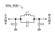
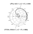
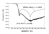
ここで比較のため、従来使用されているLPF904a,904b(図1参照)の一例を図6の回路図に示す。また、これと本実施例によるLPF4a,4bとのインピーダンス特性を図7のスミスチャートに示す。更に、GSM送信時におけるLPF4a,4bのフィルタ特性とLPF904a,904bのフィルタ特性とを図8に示す。
Here, for comparison, an example of
図7に示すように、従来使用されているLPF904a,904bは、図6に示すLPF4a,4bと同様の構成において、入出力端にインダクタL2,L3が設けられていない。また、図7に示すように、LPF4a,4bのインピーダンス特性はLPF904a,904bのインピーダンス特性と比較して無限大方向に回転している。すなわち、入出力端にインダクタL2,L3を挿入することで、それぞれのLPF4a,4bにおける周波数帯域外での入力インピーダンスが無限大となるように位相が回転していることが分かる。
As shown in FIG. 7, conventionally used
更に、図8を参照すると明らかなように、従来によるLPF904a,904bのフィルタ特性は例えば2GHz以上の周波数帯域での減衰量が悪いのに対し、本実施例によるLPF4a,4bのフィルタ特性は、この周波数帯域において良好な減衰量を実現している。このため、LPF4a,4bを用いることで製品特性が向上されていることが分かる。
Further, as apparent from FIG. 8, the filter characteristics of the
尚、上記の構成において、インダクタL2,L3は、チップ部品,配線パターン又はこれらの組み合わせ等で構成することができる。 In the above configuration, the inductors L2 and L3 can be configured by a chip component, a wiring pattern, or a combination thereof.
また、同高周波スイッチモジュール10は、消費電流の低減を目的とした回路素子を必要としないため、小型化及び低背化することができる。具体的には、図9に示すように、従来技術において例えば7.2[mm]×5.5[mm]=39.6[mm2]の大きさで作製された高周波スイッチモジュール(図1の高周波スイッチモジュール900参照)を、本実施例により6.7[mm]×5.5[mm]=36.85[mm2]の大きさで作製することができ、約7%の実装面積の削減が達成された。また、本実施例では極度の多層化を必要としないため、図9に示すように、従来技術において例えば1.8[mm]の高さで作成された高周波スイッチモジュール(同図1参照)を、本実施例により1.5[mm]とすることができ、大幅な低背化を達成できた。従って、体積比で考えると、約78%の大きさとすることができた。尚、図9は、本実施例による高周波スイッチモジュール10の外寸を示す上面図及び側面図である。但し、比較のため、従来技術による高周波スイッチモジュール900(図1参照)の外寸を図9において破線で示す。
Moreover, since the high
更に、GaAsスイッチ11Aを用いることで、PINダイオードスイッチ回路を用いた場合と比較して、特性を低下させることなく低い挿入損失の高周波スイッチモジュール10を実現することができる。
Furthermore, by using the
尚、上記構成において、GaAs11AとLPF4a,4bとBPF5a,5b及び5cとESD保護回路18とは、単一の基板上に実装され、1パッケージとして作製される。この基板には、例えばLTCC(Low Temperature Co-fired Ceramics)等のセラミック基板等を使用することが可能である。
In the above configuration, the
次に、本発明の実施例2について図面を用いて詳細に説明する。図10は、本実施例による高周波スイッチモジュール20の構成を示す回路図である。尚、以下の説明において、実施例1と同様の構成については、同一の符号を付し、その詳細な説明を省略する。また、特記しない構成に関しては実施例1と同様である。
Next, a second embodiment of the present invention will be described in detail with reference to the drawings. FIG. 10 is a circuit diagram showing the configuration of the high-
図10に示すように、本実施例による高周波スイッチモジュール20は、実施例1による高周波スイッチモジュール10と同様の構成において、GaAsスイッチ11AとBPF5a,5b及び5cとの間にそれぞれインピーダンス調整回路25a,25b及び25cが設けられた構成を有する。
As shown in FIG. 10, the high-
ここで図11に、本実施例によるインピーダンス調整回路25a,25b及び25cの回路構成を示す。図11に示すように、インピーダンス調整回路25a,25b及び25cは、入出力端子間にコンデンサC25を有して構成される。また、コンデンサC25の入力端子側は分岐され、インダクタL25を介して接地されている。
FIG. 11 shows a circuit configuration of the
このような構成を有するインピーダンス調整回路25a,25b及び25cにおいて、インダクタL25及びコンデンサC25をトリミングし、その値を調整することで、インピーダンスを調整することができる。
In the
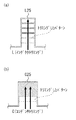
尚、インダクタL25のトリミングは、図12(a)に示すように、インダクタを形成するパターンを順次削除(トリミング)し、所望するインダクタンスを得ることで行われる。また、コンデンサC25のトリミングは、図12(b)に示すように、コンデンサの電極を形成するパターンを徐々に削除(トリミング)し、所望する静電容量を得ることが行われる。 The trimming of the inductor L25 is performed by sequentially deleting (trimming) the pattern forming the inductor to obtain a desired inductance, as shown in FIG. Further, as shown in FIG. 12B, the capacitor C25 is trimmed by gradually deleting (trimming) the pattern forming the capacitor electrode to obtain a desired capacitance.
以上のようなトリミングを行い、インダクタL25のインダクタンスとコンデンサC25の静電容量とを調整することで、GaAsスイッチ(11A)とBPF(5a,5b及び5b)との間のインピーダンスを調整することが可能となる。すなわち、PCS受信系の周波数帯域でBPF5bの入力インピーダンスが無限大となるように、DCS受信系のBPF5bに接続されたインピーダンス調整回路25bのインダクタL25及びコンデンサC25をそれぞれ選定及びトリミングし、また、DCS受信系の周波数帯域でBPF5cの入力インピーダンスが無限大となるように、PCS受信系のBPF5cに接続されたインピーダンス調整回路25cのインダクタL25及びコンデンサC25をそれぞれ選定及びトリミングする。これにより、BPFにおける挿入損失のバラツキを低減することが可能となり、結果として製品としての特性のバラツキを低減することができる。
By performing the trimming as described above and adjusting the inductance of the inductor L25 and the capacitance of the capacitor C25, the impedance between the GaAs switch (11A) and the BPF (5a, 5b, and 5b) can be adjusted. It becomes possible. That is, the inductor L25 and the capacitor C25 of the
次に、本発明の実施例3について図面を用いて詳細に説明する。図13は、本実施例による高周波スイッチモジュール30の構成を示す回路図である。尚、以下の説明において、実施例1と同様の構成については、同一の符号を付し、その詳細な説明を省略する。また、特記しない構成に関しては実施例1と同様である。 Next, Example 3 of the present invention will be described in detail with reference to the drawings. FIG. 13 is a circuit diagram showing the configuration of the high-frequency switch module 30 according to this embodiment. In the following description, the same components as those in the first embodiment are denoted by the same reference numerals, and detailed description thereof is omitted. Further, the configuration not specifically mentioned is the same as that of the first embodiment.
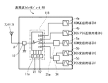
図13に示すように、本実施例による高周波スイッチモジュール30は、実施例1による高周波スイッチモジュール10と同様の構成において、GaAsスイッチ11AがGaAsスイッチ11Bに置き換えられている。GaAsスイッチ11BはGaAsスイッチ11Aと比較して、端子aの接続先となる端子の数が1つ少ない。これに伴い、端子eに接続された配線の一部がBPF5b及び5cで共用される。また、端子eに接続された配線を、BPF5b及び5cに分波するために、この配線とBPF5b及び5cの間に分波回路34が設けられている。
As shown in FIG. 13, the high frequency switch module 30 according to the present embodiment has the same configuration as that of the high
より詳細に説明する。GaAsスイッチ11Bにおいて、端子aの接続先となる端子の数は、LPF4a及び4b並びにBPF5a,5b及び5cの数よりも少ない。すなわち、切り替えるべき周波数の数に対して、端子aの接続先が不足している。尚、図13において、LPF4a及び4b並びにBPF5a,5b及び5cの数は5つであるのに対し、端子aの接続先となる端子の数は、端子b〜eの合計4つである。
This will be described in more detail. In the
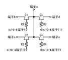
このようなGaAsスイッチ11Bは、図14に示すように、4つのFETQ1〜Q4と、これらのゲーと電極にそれぞれ設けられた抵抗R1〜R4を有して構成することができる。すなわち、実施例1で示したGaAsスイッチ11Aの回路構成(図3参照)と比較して、FET(Q5)及び抵抗(R5)が1つ少ない回路構成となり、その実装面積が縮小される。
As shown in FIG. 14, such a
但し、端子aの接続先が切り替えるべき周波数の数に対して不足している場合、端子aの接続先である端子b〜eの何れか(図13では端子e)を、例えばBPF5b及び5cで共用する必要がある。この組み合わせは、例えばBPF5a及び5bであっても、BPF5a及び5cであってもよいが、それぞれの通信システムで使用する周波数帯域を考慮して、BPF5b及び5cの組み合わせとすることが好ましい。
However, if the connection destination of the terminal a is insufficient with respect to the number of frequencies to be switched, any of the terminals b to e to which the terminal a is connected (terminal e in FIG. 13) is, for example,
また、共用した端子eに接続された配線上には分波回路34が設けられ、伝搬する高周波信号が2つの配線に分波される。換言すれば、高周波信号を分波する分波回路34を用い、これを介して2つのBPF5b,5cをGaAsスイッチ11Bにおける同一の端子eに接続した構成とすることで、より小型のGaAsスイッチを使用することが可能となるため、更なる製品の小型化を実現できる。尚、この構成によれば、実施例1と同様の動作が実現できると共に、その特性を劣化させることも無い。
Further, a
また、GaAsスイッチ11Bにおけるデコーダ11bの制御端子は、切替数が4つとなったことから、その数が2つになる。これに伴い、デコーダ11bに入力される切替電圧のビット数も2ビットとなる。ここで、制御端子V1,V2の電圧レベルとコントロール端子I〜IVの電圧レベルとのデコード対応、すなわち送受信切替ロジックの一例を表2に示す。
Further, since the number of switching of the control terminal of the
表2に示すようなロジックに従ってFETQ1〜Q4のオン/オフを切り替えることで、端子aと端子b〜eの何れかとの1対1の対応を得ることができる。すなわち、実施例1と比較して少ないビットで制御することが可能となるため、製品をより簡素化することができる。 By switching on / off the FETs Q1 to Q4 according to the logic shown in Table 2, a one-to-one correspondence between the terminal a and any of the terminals be can be obtained. That is, since it becomes possible to control with fewer bits than in the first embodiment, the product can be further simplified.
以上のように、GaAsスイッチとBPFとの間に分波回路を設けることで、本実施例によれば、GaAsスイッチの切替え端子を1つ又はそれ以上削減することが可能となり、GaAsスイッチの小型化、及び制御系の回路構成を簡素化することが可能となる。これにより、回路規模の縮小が図れるため、高周波スイッチモジュールの小型化が可能となる。 As described above, by providing a branching circuit between the GaAs switch and the BPF, according to the present embodiment, one or more switching terminals of the GaAs switch can be reduced, and the GaAs switch can be reduced in size. And the circuit configuration of the control system can be simplified. Thereby, since the circuit scale can be reduced, the high-frequency switch module can be reduced in size.
次に、本発明の実施例4について図面を用いて詳細に説明する。図15は、本実施例による高周波スイッチモジュール40の構成を示す回路図である。尚、以下の説明において、実施例2又は3と同様の構成については、同一の符号を付し、その詳細な説明を省略する。また、特記しない構成に関しては実施例1から3と同様である。 Next, a fourth embodiment of the present invention will be described in detail with reference to the drawings. FIG. 15 is a circuit diagram showing the configuration of the high-frequency switch module 40 according to this embodiment. In the following description, the same components as those in the second or third embodiment are denoted by the same reference numerals, and detailed description thereof is omitted. Further, the configuration not specifically mentioned is the same as in the first to third embodiments.
図15に示すように、本実施例による高周波スイッチモジュール40は、実施例3による高周波スイッチモジュール30において、分波回路34を介さないBPF5aとGaAsスイッチ11Bとを接続する配線上に、実施例2によるインピーダンス調整回路25aが組み込まれた構成を有する。
As shown in FIG. 15, the high-frequency switch module 40 according to the present embodiment is similar to the high-frequency switch module 30 according to the third embodiment on the wiring connecting the
このように構成することで、本実施例によれば、実施例3と同様に、GaAsスイッチの切替え端子を1つ又はそれ以上削減することが可能となり、GaAsスイッチの小型化、及び制御系の回路構成を簡素化することが可能となる。これにより、回路規模の縮小が図れるため、高周波スイッチモジュールの小型化が可能となる。また、このような効果に付帯して、実施例2と同様に、GaAsスイッチとBPFとの間のインピーダンスを調整することが可能となる。これにより、BPFにおける挿入損失のバラツキを低減することが可能となり、結果として製品としての特性のバラツキを低減することができる。 With this configuration, according to the present embodiment, as in the third embodiment, it is possible to reduce one or more switching terminals of the GaAs switch, thereby reducing the size of the GaAs switch and the control system. The circuit configuration can be simplified. Thereby, since the circuit scale can be reduced, the high-frequency switch module can be reduced in size. In addition to this effect, the impedance between the GaAs switch and the BPF can be adjusted as in the second embodiment. This makes it possible to reduce variations in insertion loss in the BPF, and as a result, variations in product characteristics can be reduced.
次に、本発明の実施例5について図面を用いて詳細に説明する。本実施例では、上記したインピーダンス調整回路25a,25b及び25cの他の構成例を示す。尚、以下の説明において、上記した実施例1から4と同様の構成については、同一の符号を付し、その詳細な説明を省略する。また、特記しない構成に関しては上記各実施例と同様である。
Next, a fifth embodiment of the present invention will be described in detail with reference to the drawings. In the present embodiment, another configuration example of the
図16は、インピーダンス調整回路25a,25b及び25cの他の構成例を示す回路図である。図16に示すように、インピーダンス調整回路25a,25b及び25cは、それぞれ伝送線路L26で構成することができる。
FIG. 16 is a circuit diagram showing another configuration example of the
この際、PCS受信系の周波数帯域でBPF5bの入力インピーダンスが無限大となるように、DCS受信系のBPF5bに接続されたインピーダンス調整回路25bの伝送線路L26を選定し、また、DCS受信系の周波数帯域でBPF5cの入力インピーダンスが無限大となるように、PCS受信系のBPF5cに接続されたインピーダンス調整回路25cの伝送線路L26を選定することが好ましい。これにより、GaAsスイッチとBPFとの間のインピーダンスを調整することが可能となる。すなわち、BPFにおける挿入損失のバラツキを低減することが可能となり、結果として製品としての特性のバラツキを低減することができる。
At this time, the transmission line L26 of the
また、伝送線路L26のインダクタは、上述において図12を用いて説明したようなトリミングを用いて調整することも可能である。これにより、個々の製品に応じた調整が可能となり、製品の品質を向上させることが可能となる。 Further, the inductor of the transmission line L26 can be adjusted by using the trimming as described above with reference to FIG. Thereby, adjustment according to each product becomes possible, and it becomes possible to improve the quality of a product.
更に、本実施例のように、インピーダンス調整回路25a,25b及び25cを伝送線路で構成することで、インダクタ及びコンデンサで構成した場合(図11参照)よりも実装面積を削減することが可能となり、結果として製品の小型化が実現できる。
Furthermore, as in this embodiment, the
次に、本発明の実施例6について図面を用いて詳細に説明する。本実施例では、GaAsスイッチ11Bを使用する構成であって、分波回路34を使用せずに端子(実施例3では端子e)を2つのBPFで共用する場合を例に挙げる。尚、以下の説明において、上記各実施例と同様の構成については、同一の符号を付し、その詳細な説明を省略する。また、特記しない構成に関しては上記各実施例と同様である。
Next,
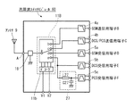
図17は、本実施例による高周波スイッチモジュール60の構成を示す回路図である。図17に示すように、高周波スイッチモジュール60は、実施例1による高周波スイッチモジュール10と同様の構成において、GaAsスイッチ11AがGaAsスイッチ11Bに置き換えられている。GaAsスイッチ11Bの端子eに接続された配線は分岐されており、その一方がDCS受信系のBPF5bに接続され、他方がインピーダンス調整回路27を介してPCS受信系のBPF5cに接続されている。
FIG. 17 is a circuit diagram showing the configuration of the high-frequency switch module 60 according to this embodiment. As shown in FIG. 17, in the high frequency switch module 60, the
インピーダンス調整回路27は、端子eとBPF5cとを接続する配線上(但し、分岐した後の配線上)に配置された伝送線路L27を有して構成される。また、伝送線路L27とBPF5cとを接続する配線は分岐され、コンデンサC27を介して接地される。
The
この構成において、伝送線路L27とコンデンサC27とは、DCS受信系の周波数帯域でBPF5cの入力インピーダンスが無限大となるように、それぞれ選定される。これにより、端子eを共用する2つの通信システムにおいて高周波信号がクロストークすることを防止でき、
また、高周波信号を分波するための分波回路34や、BPFと1対1に設けられたインピーダンス調整回路25a,25b及び25bを用いる必要が無いため、回路規模が縮小を縮小することができ、製品をより小型化することが可能となる。更に、小型のGaAsスイッチを使用できるため、実装面積を縮小でき、更なる製品の小型化が可能となる。
In this configuration, the transmission line L27 and the capacitor C27 are selected so that the input impedance of the
Further, since it is not necessary to use the
尚、上記実施例1から実施例6は本発明を実施するための例にすぎず、本発明はこれらに限定されるものではなく、これらの実施例を種々変形することは本発明の範囲内であり、更に本発明の範囲内において、他の様々な実施例が可能であることは上記記載から自明である。 In addition, the said Example 1- Example 6 is only an example for implementing this invention, this invention is not limited to these, Various deformation | transformation of these Examples is in the scope of this invention. It is obvious from the above description that various other embodiments are possible within the scope of the present invention.
4a、4b LPF
5a、5b、5c BPF
9 アンテナ
10、20、30、40、60 高周波スイッチモジュール
11A、11B GaAsスイッチ
11a、11b デコーダ
18 ESD保護回路
25a、25b、25c、27 インピーダンス調整回路
34 分波回路
A アンテナ端子
B GSM送信用端子
C DCS/PCS送信用端子
D GSM受信用端子
E DCS受信用端子
F PCS受信用端子
a〜f 端子
V1、V2、V3 制御端子
I〜V コントロール端子
C1、C2、C3、C4、C25、C27、C181、C182、C183 コンデンサ
L1、L2、L3、L25、L26、L181、L185、L186、L187 インダクタ
L27 伝送線路
Q1〜Q5 FET
R1〜R5 抵抗
4a, 4b LPF
5a, 5b, 5c BPF
9
R1-R5 resistance
Claims (13)
前記ローパスフィルタは、並列に接続された第1のインダクタ及びコンデンサと、当該ローパスフィルタの入出力側にそれぞれ設けられた第2及び第3のインダクタとを有し、
前記第2及び第3のインダクタのインダクタンスは前記第1のインダクタのインダクタンスよりも大きいことを特徴とする高周波スイッチモジュール。 A high-frequency switch module having a low-pass filter provided for each transmission system and a gallium arsenide switch that switches connection to any of the low-pass filters,
The low-pass filter has a first inductor and a capacitor connected in parallel, and second and third inductors respectively provided on the input and output sides of the low-pass filter,
The high frequency switch module according to claim 1, wherein the inductance of the second and third inductors is larger than the inductance of the first inductor.
前記砒化ガリウムスイッチは、前記ローパスフィルタ及び前記バンドパスフィルタの何れかに接続を切り替えることを特徴とする請求項1記載の高周波スイッチモジュール。 Has a bandpass filter provided for each receiving system,
The high-frequency switch module according to claim 1, wherein the gallium arsenide switch switches connection to either the low-pass filter or the band-pass filter.
前記砒化ガリウムスイッチから入力された高周波信号を分波する分波回路とを有し、
前記バンドパスフィルタの少なくとも2つが前記分波回路を介して前記砒化ガリウムスイッチにおける同一の端子に接続されていることを特徴とする請求項1記載の高周波スイッチモジュール。 A bandpass filter provided for each receiving system;
A demultiplexing circuit for demultiplexing a high-frequency signal input from the gallium arsenide switch,
2. The high frequency switch module according to claim 1, wherein at least two of the band pass filters are connected to the same terminal in the gallium arsenide switch via the branching circuit.
前記バンドパスフィルタと前記砒化ガリウムスイッチとを接続する配線の少なくとも2つは、共通化された後に前記砒化ガリウムスイッチにおける同一の端子に接続され、
共通化される前記配線の少なくとも1つにインピーダンス調整回路を有することを特徴とする請求項1記載の高周波スイッチモジュール。 Has a bandpass filter provided for each receiving system,
At least two of the wirings connecting the bandpass filter and the gallium arsenide switch are connected to the same terminal in the gallium arsenide switch after being shared,
The high-frequency switch module according to claim 1, further comprising an impedance adjustment circuit in at least one of the common wirings.
前記ローパスフィルタは全ての前記送信系に設けられていることを特徴とする請求項1から6の何れか1項に記載の高周波スイッチモジュール。 There are two transmission systems,
The high frequency switch module according to claim 1, wherein the low-pass filter is provided in all the transmission systems.
前記バンドパスフィルタは少なくとも2つの前記受信系に設けられていることを特徴とする請求項2、4又は6記載の高周波スイッチモジュール。 There are three receiving systems,
The high-frequency switch module according to claim 2, 4 or 6, wherein the band-pass filter is provided in at least two of the reception systems.
前記インダクタ,前記コンデンサ又は前記伝送線路は、インダクタンス又は静電容量をトリミングにより調整可能な導体パターンで形成されていることを特徴とする請求項3、5又は6記載の高周波スイッチモジュール。 The impedance adjustment circuit includes an inductor, a capacitor, or a transmission line,
7. The high-frequency switch module according to claim 3, wherein the inductor, the capacitor, or the transmission line is formed of a conductor pattern whose inductance or capacitance can be adjusted by trimming.
Priority Applications (4)
| Application Number | Priority Date | Filing Date | Title |
|---|---|---|---|
| JP2003354151A JP4123435B2 (en) | 2003-10-14 | 2003-10-14 | High frequency switch module |
| DE102004049808A DE102004049808A1 (en) | 2003-10-14 | 2004-10-12 | High-frequency switching module |
| US10/963,814 US7328041B2 (en) | 2003-10-14 | 2004-10-14 | High-frequency switch module |
| CNB2004100837347A CN100414845C (en) | 2003-10-14 | 2004-10-14 | High frequency switch module |
Applications Claiming Priority (1)
| Application Number | Priority Date | Filing Date | Title |
|---|---|---|---|
| JP2003354151A JP4123435B2 (en) | 2003-10-14 | 2003-10-14 | High frequency switch module |
Publications (2)
| Publication Number | Publication Date |
|---|---|
| JP2005123740A true JP2005123740A (en) | 2005-05-12 |
| JP4123435B2 JP4123435B2 (en) | 2008-07-23 |
Family
ID=34419936
Family Applications (1)
| Application Number | Title | Priority Date | Filing Date |
|---|---|---|---|
| JP2003354151A Expired - Fee Related JP4123435B2 (en) | 2003-10-14 | 2003-10-14 | High frequency switch module |
Country Status (4)
| Country | Link |
|---|---|
| US (1) | US7328041B2 (en) |
| JP (1) | JP4123435B2 (en) |
| CN (1) | CN100414845C (en) |
| DE (1) | DE102004049808A1 (en) |
Cited By (3)
| Publication number | Priority date | Publication date | Assignee | Title |
|---|---|---|---|---|
| WO2008038380A1 (en) * | 2006-09-28 | 2008-04-03 | Panasonic Corporation | Wireless communication apparatus |
| WO2010053131A1 (en) | 2008-11-05 | 2010-05-14 | 日立金属株式会社 | High-frequency circuit, high-frequency part, and multiband communication device |
| JP2011077723A (en) * | 2009-09-29 | 2011-04-14 | Murata Mfg Co Ltd | High-frequency switch module |
Families Citing this family (28)
| Publication number | Priority date | Publication date | Assignee | Title |
|---|---|---|---|---|
| EP1876721A1 (en) * | 2005-04-15 | 2008-01-09 | Hitachi Metals, Ltd. | Multi-band high-frequency circuit, multi-band high-frequency circuit component, and multi-band communication apparatus using the same |
| JP2006310904A (en) * | 2005-04-26 | 2006-11-09 | Hitachi Media Electoronics Co Ltd | Signal circuit and information processing apparatus including the same |
| EP1876722B1 (en) * | 2005-04-28 | 2016-08-24 | Murata Manufacturing Co., Ltd. | High frequency switching module and method for adjusting frequency characteristic of high frequency circuit |
| US7933561B2 (en) * | 2006-12-11 | 2011-04-26 | Apple Inc. | Wireless communications circuitry with simultaneous receive capabilities for handheld electronic devices |
| US7818029B2 (en) * | 2007-04-11 | 2010-10-19 | Apple Inc. | Wireless communications circuitry with antenna sharing capabilities for handheld electronic devices |
| DE102007021581B4 (en) * | 2007-05-08 | 2018-09-27 | Snaptrack Inc. | Electrical component with a front-end circuit |
| TWI399885B (en) * | 2007-05-22 | 2013-06-21 | Htc Corp | Radio-frequency apparatus with electrostatic protection |
| US20080291591A1 (en) * | 2007-05-22 | 2008-11-27 | High Tech Computer, Corp. | Radio-frequency apparatus with electrostatic discharge protection |
| JP5083125B2 (en) * | 2008-08-27 | 2012-11-28 | 株式会社村田製作所 | Demultiplexer, semiconductor integrated circuit device and communication portable terminal |
| CN101789777B (en) * | 2009-12-29 | 2011-08-10 | 北京大学 | Radio frequency transmitting/receiving transfer switch |
| JP5293762B2 (en) * | 2011-03-04 | 2013-09-18 | 株式会社村田製作所 | High frequency switch module |
| US9627883B2 (en) * | 2011-04-13 | 2017-04-18 | Qorvo Us, Inc. | Multiple port RF switch ESD protection using single protection structure |
| US9728532B2 (en) | 2011-04-13 | 2017-08-08 | Qorvo Us, Inc. | Clamp based ESD protection circuits |
| CN103828249B (en) * | 2011-09-26 | 2016-08-17 | 株式会社村田制作所 | High frequency module |
| WO2013119181A1 (en) * | 2012-02-06 | 2013-08-15 | Nanyang Technological University | A switch |
| CN102637964A (en) * | 2012-04-28 | 2012-08-15 | 上海华勤通讯技术有限公司 | Antenna system and mobile terminal thereof |
| KR20130127782A (en) * | 2012-05-15 | 2013-11-25 | 삼성전기주식회사 | A switching circuit and a wireless communication system including the same |
| US9313053B2 (en) * | 2012-05-15 | 2016-04-12 | Broadcom Corporation | Filter circuitry |
| TWI479953B (en) * | 2013-02-26 | 2015-04-01 | Wistron Corp | Motherboard with electrostatic discharge protection function |
| US9728330B2 (en) * | 2014-07-03 | 2017-08-08 | Ferfics Limited | Radio frequency switching system with improved linearity |
| WO2017138539A1 (en) * | 2016-02-08 | 2017-08-17 | 株式会社村田製作所 | High-frequency front-end circuit and communication device |
| US10637460B2 (en) | 2016-06-14 | 2020-04-28 | Macom Technology Solutions Holdings, Inc. | Circuits and operating methods thereof for monitoring and protecting a device |
| US20180109228A1 (en) | 2016-10-14 | 2018-04-19 | MACOM Technology Solution Holdings, Inc. | Phase shifters for gallium nitride amplifiers and related methods |
| US20190028066A1 (en) | 2017-07-24 | 2019-01-24 | Macom Technology Solutions Holdings, Inc. | Fet operational temperature determination by field plate resistance thermometry |
| US20190028065A1 (en) | 2017-07-24 | 2019-01-24 | Macom Technology Solutions Holdings, Inc. | Fet operational temperature determination by gate structure resistance thermometry |
| JP2019101735A (en) * | 2017-12-01 | 2019-06-24 | 東芝テック株式会社 | RFID tag |
| CN109861653A (en) * | 2018-12-28 | 2019-06-07 | 成都燎原星光电子有限责任公司 | A kind of circuit improving antenna-feeder system pre-low-noise amplifier antistatic effect |
| CN119543883B (en) * | 2025-01-02 | 2026-01-16 | 电子科技大学 | Adjustable N-path reflectionless filter and superheterodyne receiver |
Citations (11)
| Publication number | Priority date | Publication date | Assignee | Title |
|---|---|---|---|---|
| JPS55149518A (en) * | 1979-05-09 | 1980-11-20 | Nec Corp | Three terminal pair branching filter |
| JPS6177408A (en) * | 1984-09-21 | 1986-04-21 | Murata Mfg Co Ltd | Polar type low-pass filter |
| JPH08107326A (en) * | 1994-10-04 | 1996-04-23 | Nippon Antenna Co Ltd | Mixers and duplexers |
| JPH1155156A (en) * | 1997-08-06 | 1999-02-26 | New Japan Radio Co Ltd | Antenna switch semiconductor integrated circuit |
| JPH11284556A (en) * | 1998-03-31 | 1999-10-15 | Sony Corp | Mobile phone equipment |
| JP2002111305A (en) * | 2000-09-28 | 2002-04-12 | Kyocera Corp | Variable frequency composite filter |
| JP2002185356A (en) * | 2000-10-26 | 2002-06-28 | Epcos Ag | Front end circuit for communication terminal equipment |
| JP2003087150A (en) * | 2001-09-14 | 2003-03-20 | Matsushita Electric Ind Co Ltd | High frequency composite switch module |
| WO2003036806A1 (en) * | 2001-10-24 | 2003-05-01 | Matsushita Electric Industrial Co., Ltd. | High-frequency compound switch module and communication terminal using it |
| JP2003152588A (en) * | 2001-08-31 | 2003-05-23 | Hitachi Metals Ltd | Multiband antenna switch circuit, multiband antenna switch laminated module composite component, and communication device using the same |
| JP2003168996A (en) * | 2001-11-30 | 2003-06-13 | Matsushita Electric Ind Co Ltd | High frequency circuit device |
Family Cites Families (12)
| Publication number | Priority date | Publication date | Assignee | Title |
|---|---|---|---|---|
| JP2002064301A (en) * | 1999-03-18 | 2002-02-28 | Hitachi Metals Ltd | High frequency switch module for triple band |
| JP3711846B2 (en) | 2000-07-27 | 2005-11-02 | 株式会社村田製作所 | High frequency module and mobile communication device using the same |
| JP2002101005A (en) | 2000-09-20 | 2002-04-05 | Tdk Corp | Front-end module for triple-band portable telephone |
| JP3758157B2 (en) | 2001-04-04 | 2006-03-22 | 日立金属株式会社 | RF stage module |
| US7057472B2 (en) * | 2001-08-10 | 2006-06-06 | Hitachi Metals, Ltd. | Bypass filter, multi-band antenna switch circuit, and layered module composite part and communication device using them |
| US6985712B2 (en) * | 2001-08-27 | 2006-01-10 | Matsushita Electric Industrial Co., Ltd. | RF device and communication apparatus using the same |
| EP1341317A1 (en) * | 2001-09-21 | 2003-09-03 | Matsushita Electric Industrial Co., Ltd. | High-frequency device |
| DE10201433B4 (en) | 2002-01-16 | 2010-04-15 | Epcos Ag | Circuit arrangement, switching module with the circuit arrangement and use of the switching module |
| US7343137B2 (en) * | 2001-09-28 | 2008-03-11 | Epcos Ag | Circuit, switching module comprising the same, and use of said switching module |
| US6975841B2 (en) * | 2001-11-12 | 2005-12-13 | Matsushita Electric Industrial Co., Ltd. | Diplexer, and high-frequency switch and antenna duplexer using the same |
| CN1327733C (en) * | 2002-08-08 | 2007-07-18 | 松下电器产业株式会社 | High frequency element |
| US7076216B2 (en) * | 2002-09-17 | 2006-07-11 | Hitachi Metals, Ltd. | High-frequency device, high-frequency module and communications device comprising them |
-
2003
- 2003-10-14 JP JP2003354151A patent/JP4123435B2/en not_active Expired - Fee Related
-
2004
- 2004-10-12 DE DE102004049808A patent/DE102004049808A1/en not_active Ceased
- 2004-10-14 US US10/963,814 patent/US7328041B2/en not_active Expired - Fee Related
- 2004-10-14 CN CNB2004100837347A patent/CN100414845C/en not_active Expired - Fee Related
Patent Citations (11)
| Publication number | Priority date | Publication date | Assignee | Title |
|---|---|---|---|---|
| JPS55149518A (en) * | 1979-05-09 | 1980-11-20 | Nec Corp | Three terminal pair branching filter |
| JPS6177408A (en) * | 1984-09-21 | 1986-04-21 | Murata Mfg Co Ltd | Polar type low-pass filter |
| JPH08107326A (en) * | 1994-10-04 | 1996-04-23 | Nippon Antenna Co Ltd | Mixers and duplexers |
| JPH1155156A (en) * | 1997-08-06 | 1999-02-26 | New Japan Radio Co Ltd | Antenna switch semiconductor integrated circuit |
| JPH11284556A (en) * | 1998-03-31 | 1999-10-15 | Sony Corp | Mobile phone equipment |
| JP2002111305A (en) * | 2000-09-28 | 2002-04-12 | Kyocera Corp | Variable frequency composite filter |
| JP2002185356A (en) * | 2000-10-26 | 2002-06-28 | Epcos Ag | Front end circuit for communication terminal equipment |
| JP2003152588A (en) * | 2001-08-31 | 2003-05-23 | Hitachi Metals Ltd | Multiband antenna switch circuit, multiband antenna switch laminated module composite component, and communication device using the same |
| JP2003087150A (en) * | 2001-09-14 | 2003-03-20 | Matsushita Electric Ind Co Ltd | High frequency composite switch module |
| WO2003036806A1 (en) * | 2001-10-24 | 2003-05-01 | Matsushita Electric Industrial Co., Ltd. | High-frequency compound switch module and communication terminal using it |
| JP2003168996A (en) * | 2001-11-30 | 2003-06-13 | Matsushita Electric Ind Co Ltd | High frequency circuit device |
Cited By (7)
| Publication number | Priority date | Publication date | Assignee | Title |
|---|---|---|---|---|
| WO2008038380A1 (en) * | 2006-09-28 | 2008-04-03 | Panasonic Corporation | Wireless communication apparatus |
| WO2010053131A1 (en) | 2008-11-05 | 2010-05-14 | 日立金属株式会社 | High-frequency circuit, high-frequency part, and multiband communication device |
| JP5316544B2 (en) * | 2008-11-05 | 2013-10-16 | 日立金属株式会社 | High frequency circuit, high frequency component, and multiband communication device |
| US8803632B2 (en) | 2008-11-05 | 2014-08-12 | Hitachi Metals, Ltd. | High-frequency circuit, high-frequency device, and multiband communications apparatus |
| JP2011077723A (en) * | 2009-09-29 | 2011-04-14 | Murata Mfg Co Ltd | High-frequency switch module |
| CN102035522A (en) * | 2009-09-29 | 2011-04-27 | 株式会社村田制作所 | High-frequency switch module |
| US8466733B2 (en) | 2009-09-29 | 2013-06-18 | Murata Manufacturing Co., Ltd. | High-frequency switch module |
Also Published As
| Publication number | Publication date |
|---|---|
| CN100414845C (en) | 2008-08-27 |
| US7328041B2 (en) | 2008-02-05 |
| CN1607738A (en) | 2005-04-20 |
| JP4123435B2 (en) | 2008-07-23 |
| DE102004049808A1 (en) | 2005-06-09 |
| US20050079828A1 (en) | 2005-04-14 |
Similar Documents
| Publication | Publication Date | Title |
|---|---|---|
| JP4123435B2 (en) | High frequency switch module | |
| JP6471810B2 (en) | Demultiplexer and design method thereof | |
| CN100555861C (en) | High frequency selection circuit, high frequency module and wireless communication device | |
| CN101662267B (en) | Branching filter, semiconductor device and communication mobile terminal | |
| EP1775847B1 (en) | High frequency composite component | |
| EP2037577B1 (en) | Filter module and communication apparatus | |
| CN107733448B (en) | Switching circuit, high-frequency module, and communication device | |
| US7466211B2 (en) | High-frequency switching module and frequency-characteristic adjusting method for high-frequency circuit | |
| JP5029946B2 (en) | Switch module | |
| JP3810011B2 (en) | High frequency switch module and multilayer substrate for high frequency switch module | |
| JP2012070267A (en) | High frequency signal processor | |
| US20040248539A1 (en) | High-frequency module and communication apparatus | |
| EP1449307B1 (en) | Impedance matching circuit for a multi-band radio frequency device | |
| JP2005303940A (en) | ANTENNA SWITCH CIRCUIT, AND COMPOSITE HIGH FREQUENCY COMPONENT AND MOBILE COMMUNICATION DEVICE USING THE SAME | |
| CN107210774A (en) | On-off circuit and high-frequency model | |
| JP4465286B2 (en) | High frequency selection circuit, high frequency module, and wireless communication device | |
| US8401495B2 (en) | High-frequency module and communication apparatus using the module | |
| JP4702622B2 (en) | Switch module | |
| KR20090005039U (en) | Signal processing unit | |
| JP4702620B2 (en) | High frequency switch module | |
| JP2003152590A (en) | Antenna switch module | |
| JP4378703B2 (en) | High frequency circuit components | |
| KR101181069B1 (en) | Front End Module | |
| JP2006121211A (en) | High frequency selection circuit, high frequency module, and wireless communication device | |
| JP2007259168A (en) | Antenna switch module |
Legal Events
| Date | Code | Title | Description |
|---|---|---|---|
| A621 | Written request for application examination |
Free format text: JAPANESE INTERMEDIATE CODE: A621 Effective date: 20050909 |
|
| A977 | Report on retrieval |
Free format text: JAPANESE INTERMEDIATE CODE: A971007 Effective date: 20080115 |
|
| A131 | Notification of reasons for refusal |
Free format text: JAPANESE INTERMEDIATE CODE: A131 Effective date: 20080129 |
|
| A521 | Request for written amendment filed |
Free format text: JAPANESE INTERMEDIATE CODE: A523 Effective date: 20080331 |
|
| TRDD | Decision of grant or rejection written | ||
| A01 | Written decision to grant a patent or to grant a registration (utility model) |
Free format text: JAPANESE INTERMEDIATE CODE: A01 Effective date: 20080422 |
|
| A01 | Written decision to grant a patent or to grant a registration (utility model) |
Free format text: JAPANESE INTERMEDIATE CODE: A01 |
|
| A61 | First payment of annual fees (during grant procedure) |
Free format text: JAPANESE INTERMEDIATE CODE: A61 Effective date: 20080423 |
|
| R150 | Certificate of patent or registration of utility model |
Free format text: JAPANESE INTERMEDIATE CODE: R150 |
|
| FPAY | Renewal fee payment (event date is renewal date of database) |
Free format text: PAYMENT UNTIL: 20110516 Year of fee payment: 3 |
|
| S111 | Request for change of ownership or part of ownership |
Free format text: JAPANESE INTERMEDIATE CODE: R313111 |
|
| FPAY | Renewal fee payment (event date is renewal date of database) |
Free format text: PAYMENT UNTIL: 20110516 Year of fee payment: 3 |
|
| S111 | Request for change of ownership or part of ownership |
Free format text: JAPANESE INTERMEDIATE CODE: R313113 |
|
| R350 | Written notification of registration of transfer |
Free format text: JAPANESE INTERMEDIATE CODE: R350 |
|
| FPAY | Renewal fee payment (event date is renewal date of database) |
Free format text: PAYMENT UNTIL: 20110516 Year of fee payment: 3 |
|
| R350 | Written notification of registration of transfer |
Free format text: JAPANESE INTERMEDIATE CODE: R350 |
|
| FPAY | Renewal fee payment (event date is renewal date of database) |
Free format text: PAYMENT UNTIL: 20110516 Year of fee payment: 3 |
|
| FPAY | Renewal fee payment (event date is renewal date of database) |
Free format text: PAYMENT UNTIL: 20120516 Year of fee payment: 4 |
|
| FPAY | Renewal fee payment (event date is renewal date of database) |
Free format text: PAYMENT UNTIL: 20130516 Year of fee payment: 5 |
|
| R250 | Receipt of annual fees |
Free format text: JAPANESE INTERMEDIATE CODE: R250 |
|
| R250 | Receipt of annual fees |
Free format text: JAPANESE INTERMEDIATE CODE: R250 |
|
| LAPS | Cancellation because of no payment of annual fees |