JP2005123799A - Piezoelectric oscillation circuit - Google Patents
Piezoelectric oscillation circuit Download PDFInfo
- Publication number
- JP2005123799A JP2005123799A JP2003355258A JP2003355258A JP2005123799A JP 2005123799 A JP2005123799 A JP 2005123799A JP 2003355258 A JP2003355258 A JP 2003355258A JP 2003355258 A JP2003355258 A JP 2003355258A JP 2005123799 A JP2005123799 A JP 2005123799A
- Authority
- JP
- Japan
- Prior art keywords
- oscillation circuit
- oscillation signal
- oscillation
- circuit
- inverter
- Prior art date
- Legal status (The legal status is an assumption and is not a legal conclusion. Google has not performed a legal analysis and makes no representation as to the accuracy of the status listed.)
- Withdrawn
Links
- 230000010355 oscillation Effects 0.000 title claims abstract description 113
- 239000003990 capacitor Substances 0.000 claims abstract description 8
- 239000004065 semiconductor Substances 0.000 claims abstract description 6
- 230000003321 amplification Effects 0.000 claims abstract description 3
- 238000003199 nucleic acid amplification method Methods 0.000 claims abstract description 3
- 230000002159 abnormal effect Effects 0.000 abstract description 23
- 239000013078 crystal Substances 0.000 abstract description 15
- 230000008878 coupling Effects 0.000 abstract description 6
- 238000010168 coupling process Methods 0.000 abstract description 6
- 238000005859 coupling reaction Methods 0.000 abstract description 6
- 230000000630 rising effect Effects 0.000 description 5
- 230000003071 parasitic effect Effects 0.000 description 4
- 238000010586 diagram Methods 0.000 description 3
- 230000010356 wave oscillation Effects 0.000 description 3
- 230000007423 decrease Effects 0.000 description 2
- 238000007599 discharging Methods 0.000 description 2
- 230000000694 effects Effects 0.000 description 2
- 238000012887 quadratic function Methods 0.000 description 2
- 230000010354 integration Effects 0.000 description 1
Images
Landscapes
- Oscillators With Electromechanical Resonators (AREA)
Abstract
【課題】 従来の圧電発振回路では、静電結合によって異常な発振信号が生じ、本来得るべき発振信号が得られないという問題があった。
【解決手段】 本発明に係る圧電発振回路は、水晶振動子Xを接続するためのパッドXG及びXDと、出力信号を取り出すためのパッドOUTを有する半導体チップ上に形成され、インバータIV1及びコンデンサCg、Cdを含んで水晶振動子Xを励振するコルピッツ型の発振回路Oscと、発振回路OscとパッドOUT間に縦続接続された複数段の反転増幅器を含む増幅回路Ampとを有する圧電発振回路であって、前記反転増幅器の縦続接続段数を奇数としている。
【選択図】 図1
PROBLEM TO BE SOLVED: In a conventional piezoelectric oscillation circuit, there is a problem that an abnormal oscillation signal is generated by electrostatic coupling, and an oscillation signal that should be originally obtained cannot be obtained.
A piezoelectric oscillation circuit according to the present invention is formed on a semiconductor chip having pads XG and XD for connecting a crystal resonator X and a pad OUT for extracting an output signal, and includes an inverter IV1 and a capacitor Cg. , A Colpitts oscillation circuit Osc including Cd for exciting the crystal resonator X, and an amplification circuit Amp including a plurality of inverting amplifiers cascaded between the oscillation circuit Osc and the pad OUT. Thus, the number of cascade connection stages of the inverting amplifier is an odd number.
[Selection] Figure 1
Description
本発明は、水晶振動子のような圧電振動子を用いた圧電発振回路に関する。 The present invention relates to a piezoelectric oscillation circuit using a piezoelectric vibrator such as a crystal vibrator.
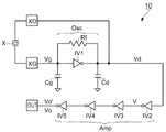
図3は、半導体チップ上に形成された従来の圧電発振回路の構成を示す回路図である。 FIG. 3 is a circuit diagram showing a configuration of a conventional piezoelectric oscillation circuit formed on a semiconductor chip.
従来の圧電発振回路10は、図3に示されるように、パッドXG及びXDを介して圧電振動子である水晶振動子Xと接続されており、水晶振動子Xを励振する発振回路Oscと、発振回路Oscから出力される発振信号Vdを増幅して、パッドOUTに発振信号Voを出力する増幅回路Ampとを含む。
As shown in FIG. 3, the conventional
発振回路Oscは、インバータIV1と、コンデンサCg、Cdとから構成される。インバータIV1には、一対のPチャネルMOSトランジスタ及びNチャネルMOSトランジスタからなるCMOSインバータが用いられる。あるいは、1つを除いた残りの入力端子を定電位に接続して、等価的にインバータ動作を可能としたNANDゲートやNORゲートであってもよい。 The oscillation circuit Osc includes an inverter IV1 and capacitors Cg and Cd. As the inverter IV1, a CMOS inverter including a pair of P-channel MOS transistors and N-channel MOS transistors is used. Alternatively, it may be a NAND gate or a NOR gate in which the remaining input terminals except for one are connected to a constant potential to enable an inverter operation equivalently.
ここで、インバータIV1は、入力端子及び出力端子が抵抗器Rfで結ばれているため、電源が投入されると同時にインバータIV1自身によって所定の直流動作点(通常は正負電源電圧の中心値)までバイアスされ、ほぼ線形な反転型の電圧−電流変換器として動作を開始する。抵抗器Rfの抵抗値は、通常、数100kΩ〜数MΩの十分に大きな値であることが多く、交流信号に対しては、その影響を無視することができる。このような回路はコルピッツ型発振回路として広く知られており、例えば、下記の特許文献1などにも詳細な記載がある。 Here, since the input terminal and the output terminal of the inverter IV1 are connected by the resistor Rf, when the power is turned on, the inverter IV1 itself reaches a predetermined DC operating point (usually the central value of the positive and negative power supply voltage). Biased and begins operation as a nearly linear inverting voltage-to-current converter. The resistance value of the resistor Rf is usually a sufficiently large value of several hundred kΩ to several MΩ, and the influence on the AC signal can be ignored. Such a circuit is widely known as a Colpitts type oscillation circuit, and for example, there is a detailed description in Patent Document 1 below.
増幅回路Ampは、縦続接続された4つのインバータIV2〜IV5からなり、発振回路Oscから出力される発振信号Vdを順次反転増幅して、発振信号Vdと同位相の発振信号VoをパッドOUTに出力する。IV2〜IV5の各インバータの出力電流は、パッドOUTに向かうにつれて徐々に増やされており、最終段のインバータIV5の出力電流は、パッドOUTに接続される所定の負荷容量を駆動できるだけの十分な値とされている。このため、増幅回路Ampには、複数段の縦続接続されたインバータが必要となる。発振信号Vdは、増幅回路Ampで増幅された後、発振信号VoとしてパッドOUTから出力される。
しかしながら、上記した従来の圧電発振回路10では、半導体チップ上でパッドOUTとパッドXGが近接した位置に設けられていると、両パッド間に静電結合が生じてしまい、これが原因となって、水晶振動子Xの共振周波数と無関係な異常発振が生じる危険性がある。集積化が進み、半導体チップが小型化された近年にあっては、この危険性は増加傾向にある。
However, in the conventional
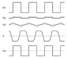
このような従来の圧電発振回路の異常発振動作を、図4に基づいて説明する。図4において、点線で示した電圧レベルは、回路の直流動作点(ここでは、正負電源電圧の中心値と仮定)を表している。まず、パッドOUTから方形波の異常な発振信号Voが出力されたと仮定する。このとき、パッドOUTとパッドXGとの間に静電結合が存在すると、異常な発振信号Voに起因して、小振幅の発振信号VgがパッドXGに生起する。発振信号Vgは、発振回路OscのインバータIV1を動作させ、インバータIV1は、発振信号Vgと位相が逆で、ほぼ同一形状の方形波の電流を出力する。この電流によってコンデンサCdが充放電されるため、図4に示した三角波の発振信号Vdが出力される。 An abnormal oscillation operation of such a conventional piezoelectric oscillation circuit will be described with reference to FIG. In FIG. 4, the voltage level indicated by the dotted line represents the DC operating point of the circuit (here, assumed to be the center value of the positive and negative power supply voltages). First, it is assumed that a square wave abnormal oscillation signal Vo is output from the pad OUT. At this time, if electrostatic coupling exists between the pad OUT and the pad XG, an oscillation signal Vg having a small amplitude is generated in the pad XG due to the abnormal oscillation signal Vo. The oscillation signal Vg causes the inverter IV1 of the oscillation circuit Osc to operate, and the inverter IV1 outputs a square-wave current having substantially the same shape as that of the oscillation signal Vg. Since the capacitor Cd is charged and discharged by this current, the triangular wave oscillation signal Vd shown in FIG. 4 is output.
さらに、発振信号Vdは、インバータIV2を動作させ、インバータIV2は、発振信号Vdと位相が逆で、ほぼ同一形状の三角波の電流を出力する。この電流によってインバータIV2の出力に存在する寄生容量(図示せず)が充放電されるため、図4に示した発振信号Vが出力される。発振信号Vの立ち上がり及び立ち下がりは、ほぼ二次関数の軌跡に沿って変化するが、インバータIV2の出力に存在する寄生容量は大きくないため、充放電が速やかに完了して、方形波に近い波形となる。このとき、発振信号Voの周波数によっては、発振信号Vが直流動作点と交差する立ち上がり(または立ち下がり)タイミングが、発振信号Voが直流動作点と交差する立ち下がり(または立ち上がり)タイミングよりも僅かに早い状態となり得る。 Further, the oscillation signal Vd causes the inverter IV2 to operate, and the inverter IV2 outputs a triangular wave current having a phase opposite to that of the oscillation signal Vd and substantially the same shape. Since this current charges and discharges a parasitic capacitance (not shown) present at the output of the inverter IV2, the oscillation signal V shown in FIG. 4 is output. The rising and falling edges of the oscillation signal V change substantially along the locus of the quadratic function, but since the parasitic capacitance present in the output of the inverter IV2 is not large, charging / discharging is completed quickly and is close to a square wave. It becomes a waveform. At this time, depending on the frequency of the oscillation signal Vo, the rising (or falling) timing at which the oscillation signal V intersects the DC operating point is slightly lower than the falling (or rising) timing at which the oscillation signal Vo intersects the DC operating point. Can be in an early state.
その後、発振信号Vは、さらに3段のインバータIV3〜IV5で増幅されて、位相が反転した方形波の発振信号Vo’に波形整形されるが、その際、当該インバータ3段分の伝播遅延量が前述のタイミング差に一致すると、発振信号Vo’は、元の異常な発振信号Voとまったく一致した波形となる。このような状態に陥ると、正帰還が確立し、異常な発振信号Voは安定して持続してしまう。 Thereafter, the oscillation signal V is further amplified by three-stage inverters IV3 to IV5 and shaped into a square-wave oscillation signal Vo ′ whose phase is inverted. At this time, the propagation delay amount corresponding to the three stages of the inverter Is equal to the above-described timing difference, the oscillation signal Vo ′ has a waveform that exactly matches the original abnormal oscillation signal Vo. In such a state, positive feedback is established, and the abnormal oscillation signal Vo is stably maintained.
以上の説明から判るように、上述の異常発振は、水晶振動子Xと何ら関係なく成立しており、発振信号Voの周波数は、水晶振動子の共振周波数とは無関係な周波数である。このとき、水晶振動子Xは高いインピーダンスを示して、回路動作から切り離された状態となっている。ひとたび、このような異常発振が生起すると、水晶振動子は回路動作から切り離されたままとなり、水晶振動子の共振周波数における所望の発振信号は得ることができない。 As can be seen from the above description, the abnormal oscillation described above is established regardless of the crystal resonator X, and the frequency of the oscillation signal Vo is a frequency that is unrelated to the resonance frequency of the crystal resonator. At this time, the crystal unit X exhibits high impedance and is in a state of being disconnected from the circuit operation. Once such abnormal oscillation occurs, the crystal resonator remains disconnected from the circuit operation, and a desired oscillation signal at the resonance frequency of the crystal resonator cannot be obtained.
上記した課題を解決すべく、本発明に係る圧電発振回路は、圧電振動子を接続するための第1及び第2のパッドと、出力信号を取り出すための第3のパッドを有する半導体チップ上に形成され、少なくとも1個のインバータ及び2個のコンデンサを含んで前記圧電振動子を励振するコルピッツ型の発振回路と、前記発振回路と前記第3のパッド間に縦続接続された複数段の反転増幅器を含む増幅回路とを有する圧電発振回路であって、前記反転増幅器の縦続接続段数が奇数であることを特徴とする。 In order to solve the above-described problems, a piezoelectric oscillation circuit according to the present invention is provided on a semiconductor chip having first and second pads for connecting a piezoelectric vibrator and a third pad for taking out an output signal. A Colpitts-type oscillation circuit formed and including at least one inverter and two capacitors to excite the piezoelectric vibrator, and a plurality of inverting amplifiers cascaded between the oscillation circuit and the third pad A piezoelectric oscillation circuit including an amplifier circuit including: an inverting amplifier having an odd number of cascade connection stages.
本発明に係る圧電発振回路によれば、増幅回路が、縦続接続された奇数個の反転増幅器から構成されていることから、パッドOUTとパッドXGとの間に静電結合が生じたとしても、前述した正帰還が確立することがなく、水晶振動子Xの共振周波数と無関係な異常発振の発生を回避することが可能になる。 According to the piezoelectric oscillation circuit of the present invention, since the amplification circuit is composed of an odd number of inverting amplifiers connected in cascade, even if electrostatic coupling occurs between the pad OUT and the pad XG, The positive feedback described above is not established, and it is possible to avoid the occurrence of abnormal oscillation unrelated to the resonance frequency of the crystal unit X.
本発明に係る圧電発振回路の実施例について、図面を参照して説明する。 Embodiments of a piezoelectric oscillation circuit according to the present invention will be described with reference to the drawings.
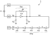
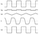
図1は、実施例の圧電発振回路の構成を示す回路図であり、図2は、実施例の圧電発振回路によって得られる効果を説明するための波形図である。 FIG. 1 is a circuit diagram showing the configuration of the piezoelectric oscillation circuit of the embodiment, and FIG. 2 is a waveform diagram for explaining the effects obtained by the piezoelectric oscillation circuit of the embodiment.
実施例の圧電発振回路1は、図1に示されるように、パッドXG及びXDを介して圧電振動子である水晶振動子Xと接続されており、水晶振動子Xを励振する発振回路Oscと、発振回路Oscから出力される発振信号Vdを増幅して、パッドOUTに発振信号Voを出力する増幅回路Ampとを含む。また、発振回路Oscは、インバータIV1と、コンデンサCg、Cdと、抵抗器Rfとからなり、増幅回路Ampは、インバータIVa、IV2〜IV5からなる。即ち、実施例1の圧電発振回路1の構成を示す図1と従来の圧電発振回路10の構成を示す図3との比較から明らかなように、実施例の圧電発振回路1は、従来の圧電発振回路10に比較して、インバータIVaが追加されており、これにより、増幅回路Ampが、合計5つのインバータIVa、IV2〜IV5を有する点のみが異なっている。従って、従来の圧電発振回路10と同一の部分については、説明の重複を避けることとする。
As shown in FIG. 1, the piezoelectric oscillation circuit 1 of the embodiment is connected to a crystal resonator X that is a piezoelectric resonator via pads XG and XD, and an oscillation circuit Osc that excites the crystal resonator X. And an amplifier circuit Amp that amplifies the oscillation signal Vd output from the oscillation circuit Osc and outputs the oscillation signal Vo to the pad OUT. The oscillation circuit Osc includes an inverter IV1, capacitors Cg and Cd, and a resistor Rf, and the amplifier circuit Amp includes inverters IVa and IV2 to IV5. That is, as is clear from a comparison between FIG. 1 showing the configuration of the piezoelectric oscillation circuit 1 of the first embodiment and FIG. 3 showing the configuration of the conventional
次に、図2を用いて、インバータIVaが追加されたことによる効果を説明する。図2において、点線で示した電圧レベルは、回路の直流動作点(ここでは、正負電源電圧の中心値と仮定)を表している。まず、パッドOUTから方形波の異常な発振信号Voが出力されたと仮定する。このとき、パッドOUTとパッドXGとの間に静電結合が存在すると、異常な発振信号Voに起因して、小振幅の発振信号VgがパッドXGに生起する。発振信号Vgは、発振回路OscのインバータIV1を動作させ、インバータIV1は、発振信号Vgと位相が逆で、ほぼ同一形状の方形波の電流を出力する。この電流によってコンデンサCdが充放電されるため、図2に示した三角波の発振信号Vdが出力される。 Next, the effect obtained by adding the inverter IVa will be described with reference to FIG. In FIG. 2, the voltage level indicated by the dotted line represents the DC operating point of the circuit (here, assumed to be the center value of the positive and negative power supply voltages). First, it is assumed that a square wave abnormal oscillation signal Vo is output from the pad OUT. At this time, if electrostatic coupling exists between the pad OUT and the pad XG, an oscillation signal Vg having a small amplitude is generated in the pad XG due to the abnormal oscillation signal Vo. The oscillation signal Vg causes the inverter IV1 of the oscillation circuit Osc to operate, and the inverter IV1 outputs a square-wave current having substantially the same shape as that of the oscillation signal Vg. Since the capacitor Cd is charged and discharged by this current, the triangular wave oscillation signal Vd shown in FIG. 2 is output.
さらに、発振信号Vdは、インバータIVaを動作させ、インバータIVaは、発振信号Vdと位相が逆で、ほぼ同一形状の三角波の電流を出力する。この電流によってインバータIVaの出力に存在する寄生容量(図示せず)が充放電されるため、図2に示した発振信号Vが出力される。発振信号Vの立ち上がり及び立ち下がりは、ほぼ二次関数の軌跡に沿って変化するが、インバータIVaの出力に存在する寄生容量は大きくないため、充放電が速やかに完了して、方形波に近い波形となる。このとき、発振信号Vが直流動作点と交差する立ち上がり(または立ち下がり)タイミングは、発振信号Voが直流動作点と交差する立ち下がり(または立ち上がり)タイミングと近くなる。 Further, the oscillation signal Vd operates the inverter IVa, and the inverter IVa outputs a triangular wave current having the same shape as that of the oscillation signal Vd. This current charges and discharges a parasitic capacitance (not shown) present in the output of the inverter IVa, so that the oscillation signal V shown in FIG. 2 is output. The rise and fall of the oscillation signal V change substantially along the locus of the quadratic function, but since the parasitic capacitance present in the output of the inverter IVa is not large, charging / discharging is completed quickly and is close to a square wave. It becomes a waveform. At this time, the rising (or falling) timing at which the oscillation signal V intersects the DC operating point is close to the falling (or rising) timing at which the oscillation signal Vo intersects the DC operating point.
その後、発振信号Vは、さらに4段のインバータIV2〜IV5で増幅されて方形波の発振信号Vo’に波形整形され、元の異常な発振信号Voとほぼ位相が反転した波形となる。このような状態では、異常な発振信号Voは帰還されてきた発振信号Vo’によって打ち消されてしまい、安定して持続することができない。 Thereafter, the oscillation signal V is further amplified by the four-stage inverters IV2 to IV5 and shaped into a square wave oscillation signal Vo ', resulting in a waveform whose phase is substantially inverted from that of the original abnormal oscillation signal Vo. In such a state, the abnormal oscillation signal Vo is canceled by the feedback oscillation signal Vo 'and cannot be stably maintained.
なお、異常な発振信号Voの周波数が極めて高い場合には、増幅器Amp内部の伝播遅延によって、発振信号Vo’の位相がちょうど反転し、元の異常な発振信号Voの位相と一致してしまうことが考えられる。しかしながら、例えこのような状態になったとしても、異常な発振信号Voが安定して持続することは難しい。なぜならば、異常な発振信号Voの周波数が高くなるにつれて、発振信号Vdの振幅が小さくなり、結果として発振信号Vo’の振幅も小さくなる。すると、発振信号Vo’の振幅は、元の異常な発振信号Voの振幅と同一にならず、小さくなってしまう。このような状態では、異常な発振信号Voは、徐々に減衰してしまい、安定して持続することはできないのである。 When the frequency of the abnormal oscillation signal Vo is extremely high, the phase of the oscillation signal Vo ′ is just inverted by the propagation delay inside the amplifier Amp, and coincides with the phase of the original abnormal oscillation signal Vo. Can be considered. However, even in such a state, it is difficult for the abnormal oscillation signal Vo to be stably maintained. This is because the amplitude of the oscillation signal Vd decreases as the frequency of the abnormal oscillation signal Vo increases, and as a result, the amplitude of the oscillation signal Vo ′ also decreases. Then, the amplitude of the oscillation signal Vo ′ is not the same as the amplitude of the original abnormal oscillation signal Vo, and becomes small. In such a state, the abnormal oscillation signal Vo gradually attenuates and cannot be stably maintained.
上述したように、実施例の圧電発振回路1では、発振回路Oscに後続する増幅回路Ampが、直列接続された5つのインバータIVa、IV2〜IV5から構成されている。これにより、増幅回路Ampの出力端子側のパッドOUTから出力された異常な発振信号Voが、静電結合によって、発振回路Oscの入力端子側のパッドXGに誘起されたとしても、最終的にパッドOUTに帰還されて出力される発振信号Vo’の位相は、元の異常な発振信号Voとほぼ逆相関係になる。従って、異常な発振信号Voが正帰還によって安定な発振を持続することはなくなり、この結果、実施例の圧電発振回路1は、水晶振動子Xの共振周波数で規定される本来の周波数で発振することが可能になる。 As described above, in the piezoelectric oscillation circuit 1 according to the embodiment, the amplifier circuit Amp subsequent to the oscillation circuit Osc includes the five inverters IVa and IV2 to IV5 connected in series. As a result, even if the abnormal oscillation signal Vo output from the pad OUT on the output terminal side of the amplifier circuit Amp is induced by the electrostatic coupling to the pad XG on the input terminal side of the oscillation circuit Osc, finally the pad The phase of the oscillation signal Vo ′ that is fed back and output to OUT is almost in reverse phase with the original abnormal oscillation signal Vo. Therefore, the abnormal oscillation signal Vo does not continue stable oscillation due to positive feedback, and as a result, the piezoelectric oscillation circuit 1 of the embodiment oscillates at an original frequency defined by the resonance frequency of the crystal resonator X. It becomes possible.
1 圧電発振回路
X 水晶振動子
Osc 発振回路
Amp 増幅回路
IVa、IV1〜IV5 インバータ
Cg、Cd コンデンサ
Rf 抵抗器
DESCRIPTION OF SYMBOLS 1 Piezoelectric oscillation circuit X Crystal oscillator Osc Oscillation circuit Amp Amplifier circuit IVa, IV1-IV5 Inverter Cg, Cd Capacitor Rf Resistor
Claims (1)
Formed on a semiconductor chip having first and second pads for connecting a piezoelectric vibrator and a third pad for taking out an output signal, including at least one inverter and two capacitors; A piezo-oscillation circuit comprising: a Colpitts oscillation circuit for exciting a piezoelectric vibrator; and an amplification circuit including a plurality of stages of inverting amplifiers connected in cascade between the oscillation circuit and the third pad, the inverting amplifier A piezoelectric oscillation circuit characterized in that the number of cascade connection stages is an odd number.
Priority Applications (1)
| Application Number | Priority Date | Filing Date | Title |
|---|---|---|---|
| JP2003355258A JP2005123799A (en) | 2003-10-15 | 2003-10-15 | Piezoelectric oscillation circuit |
Applications Claiming Priority (1)
| Application Number | Priority Date | Filing Date | Title |
|---|---|---|---|
| JP2003355258A JP2005123799A (en) | 2003-10-15 | 2003-10-15 | Piezoelectric oscillation circuit |
Publications (1)
| Publication Number | Publication Date |
|---|---|
| JP2005123799A true JP2005123799A (en) | 2005-05-12 |
Family
ID=34612918
Family Applications (1)
| Application Number | Title | Priority Date | Filing Date |
|---|---|---|---|
| JP2003355258A Withdrawn JP2005123799A (en) | 2003-10-15 | 2003-10-15 | Piezoelectric oscillation circuit |
Country Status (1)
| Country | Link |
|---|---|
| JP (1) | JP2005123799A (en) |
-
2003
- 2003-10-15 JP JP2003355258A patent/JP2005123799A/en not_active Withdrawn
Similar Documents
| Publication | Publication Date | Title |
|---|---|---|
| US8232847B2 (en) | Oscillation circuit | |
| US9461632B2 (en) | Oscillator circuit | |
| JP2002344242A (en) | Voltage-controlled oscillator | |
| JP5048355B2 (en) | Oscillator circuit | |
| JP6829824B2 (en) | Oscillator circuit using a comparator | |
| CN103001582B (en) | Semiconductor device | |
| US12184234B2 (en) | Semiconductor device | |
| US7511584B2 (en) | Voltage controlled oscillator capable of operating in a wide frequency range | |
| JP2005123799A (en) | Piezoelectric oscillation circuit | |
| JPH0870241A (en) | Delay circuit | |
| JP2003110361A (en) | Crystal oscillator circuit | |
| US6690245B2 (en) | Oscillation control circuit | |
| JP6788850B2 (en) | Comparator and oscillator circuit using the comparator | |
| JPS59175218A (en) | CMOS inverter | |
| KR20030072527A (en) | Generator of dc-dc converter | |
| JP2012105007A (en) | Power-on reset circuit | |
| CN101635565A (en) | Oscillation detection circuit | |
| JPH0575343A (en) | Clock signal output circuit | |
| JPH11284438A (en) | Piezoelectric oscillator | |
| JP6786968B2 (en) | Oscillator circuit using a comparator | |
| US20240388253A1 (en) | Reducing Startup Time In A Crystal Oscillator | |
| JP2684513B2 (en) | Oscillation integrated circuit and oscillation circuit | |
| JP3917902B2 (en) | Oscillator circuit | |
| JPH0353705A (en) | Semiconductor integrated circuit | |
| JPH0697732A (en) | Oscillation circuit |
Legal Events
| Date | Code | Title | Description |
|---|---|---|---|
| A621 | Written request for application examination |
Effective date: 20060929 Free format text: JAPANESE INTERMEDIATE CODE: A621 |
|
| RD04 | Notification of resignation of power of attorney |
Free format text: JAPANESE INTERMEDIATE CODE: A7424 Effective date: 20070403 |
|
| A131 | Notification of reasons for refusal |
Effective date: 20090728 Free format text: JAPANESE INTERMEDIATE CODE: A131 |
|
| A761 | Written withdrawal of application |
Effective date: 20090924 Free format text: JAPANESE INTERMEDIATE CODE: A761 |