JP2005129727A - Multilayer wiring board and manufacturing method thereof - Google Patents
Multilayer wiring board and manufacturing method thereof Download PDFInfo
- Publication number
- JP2005129727A JP2005129727A JP2003363712A JP2003363712A JP2005129727A JP 2005129727 A JP2005129727 A JP 2005129727A JP 2003363712 A JP2003363712 A JP 2003363712A JP 2003363712 A JP2003363712 A JP 2003363712A JP 2005129727 A JP2005129727 A JP 2005129727A
- Authority
- JP
- Japan
- Prior art keywords
- wiring board
- conductive particles
- wiring pattern
- wiring
- multilayer wiring
- Prior art date
- Legal status (The legal status is an assumption and is not a legal conclusion. Google has not performed a legal analysis and makes no representation as to the accuracy of the status listed.)
- Pending
Links
Images
Landscapes
- Production Of Multi-Layered Print Wiring Board (AREA)
Abstract
【課題】層間接続の信頼性が高い多層配線基板及びその製造方法を提供する。
【解決手段】配線パターンを形成する金属箔1に粗化処理し、凹凸部を形成する(a)。粗化処理された金属箔1と基材となる熱可塑性樹脂フィルム2とを熱融着や接着等により貼着し(b)、金属箔1をエッチング等により、配線パターンを形成する(c)。配線パターンが形成された基板の熱可塑性樹脂フィルム2側から炭酸ガスレーザ等により有底ビアホール4を形成する(d)。そして、基材に形成された有底ビアホール4に導電性粒子5を充填する(e)。この単一配線基板を複数枚重ねて、上下両面から真空熱プレス機により一括積層して多層配線板を製造する(f)。
【選択図】図1
A multilayer wiring board with high reliability of interlayer connection and a method for manufacturing the same are provided.
A metal foil for forming a wiring pattern is roughened to form a concavo-convex portion (a). The roughened metal foil 1 and the thermoplastic resin film 2 serving as a base material are attached by thermal fusion or adhesion (b), and the metal foil 1 is etched to form a wiring pattern (c). . A bottomed via hole 4 is formed by a carbon dioxide laser from the thermoplastic resin film 2 side of the substrate on which the wiring pattern is formed (d). Then, the conductive particles 5 are filled into the bottomed via hole 4 formed in the base material (e). A plurality of the single wiring boards are stacked, and a multilayer wiring board is manufactured by stacking them together from above and below using a vacuum heat press (f).
[Selection] Figure 1
Description
本発明は、絶縁基材に熱可塑性樹脂を用いた多層配線基板及びその製造方法に関する。 The present invention relates to a multilayer wiring board using a thermoplastic resin as an insulating base material and a method for manufacturing the same.
従来、多層配線基板の製造方法は、配線パターンと層間接続部(ビア)が形成された単一配線基板を一層ずつ積み重ねて層間接続を行う積層加工を繰り返していた(シーケンシャル工法)。しかし、このような工法では、工程数が積層数分増加してしまうため、生産性と歩留まりに問題があった。 Conventionally, a multilayer wiring board manufacturing method has repeatedly performed a laminating process in which a single wiring board on which a wiring pattern and interlayer connection portions (vias) are formed is stacked layer by layer to perform interlayer connection (sequential method). However, such a method has a problem in productivity and yield because the number of steps increases by the number of layers.
この問題に対し、熱可塑性樹脂からなる絶縁基材を使用することにより一括融着多層化する方法が提案されている(例えば、特許文献1参照)。その方法は、ビアに導電性ペーストを充填し、ビアの導電性ペーストと配線金属との間で金属拡散させることにより層間接続させる。しかし、このビア接続に金属拡散を利用する方法は高温状態に長く保つ必要があるため生産性が低くなりがちである。さらに特許文献1の如く配線金属が銅であり、導電性ペースト内の導電性粒子がスズと銀であるような場合、スズと配線の銅との金属間化合物層は脆く、層を適切な厚みになるようにコントロールしないと接続部分の強度が低下し信頼性が低下するおそれがある。しかし、層の厚みをコントロールすることは容易ではない。 In order to solve this problem, a method has been proposed in which an insulating base material made of a thermoplastic resin is used to form a multi-layer by simultaneous fusion (see, for example, Patent Document 1). In this method, the via is filled with a conductive paste, and the interlayer connection is made by metal diffusion between the conductive paste of the via and the wiring metal. However, the method using metal diffusion for this via connection tends to be low in productivity because it needs to be kept at a high temperature for a long time. Furthermore, when the wiring metal is copper as in Patent Document 1 and the conductive particles in the conductive paste are tin and silver, the intermetallic compound layer of tin and copper of the wiring is brittle, and the layer has an appropriate thickness. If the control is not performed, the strength of the connection portion is lowered and the reliability may be lowered. However, it is not easy to control the thickness of the layer.
また、金属拡散ではなく圧接により導通を得る工法があるが、一括積層では基材自体が圧力を吸収してしまい十分な圧力が伝わらないため、導通を得るのに比較的高い圧力が必要となる。また、うまく力が伝わってもビアが硬いので配線が変形したり、傾いたりしてしまうおそれがある。 In addition, there is a method of obtaining conduction by pressure welding rather than metal diffusion, but in the case of batch lamination, since the base material itself absorbs pressure and sufficient pressure is not transmitted, relatively high pressure is required to obtain conduction. . Even if the force is transmitted well, the vias are hard and the wiring may be deformed or tilted.
本発明は、上記問題点を解決するためになされたものであり、比較的低圧で積層しても、層間接続の信頼性が高い多層配線基板及びその製造方法を提供することを目的とする。 The present invention has been made to solve the above-described problems, and an object of the present invention is to provide a multilayer wiring board having high interlayer connection reliability even when laminated at a relatively low pressure, and a method for manufacturing the same.
そこで、上述した目的を達成するために、本発明に係る多層配線基板は、熱可塑性樹脂からなる絶縁基材に配線パターンと、層間接続部とを設けた単一配線基板が複数枚積層されたものであって、複数枚の単一配線基板を加熱加圧することにより他の単一配線基板と融着して形成された多層配線基板において、配線パターンには、表面に凹凸部が形成されおり、層間接続部には、導電性粒子が充填されている。ここで、導電性粒子は、配線パターンの表面に形成された凹凸部の凹部に入り込まない大きさである。また、導電性粒子は、配線パターンの材料よりも硬度が同等若しくは低い材料からなる。さらに、上記層間接続部において、凹凸部の凸部は、導電性粒子に挿入若しくは包まれており、凹凸部と導電性粒子との隙間及び導電性粒子同士の隙間に熱化塑性樹脂が入り込んでいる。 Therefore, in order to achieve the above-described object, a multilayer wiring board according to the present invention is formed by laminating a plurality of single wiring boards provided with a wiring pattern and an interlayer connection portion on an insulating base material made of a thermoplastic resin. In a multilayer wiring board formed by fusing with other single wiring boards by heating and pressing a plurality of single wiring boards, the wiring pattern has an uneven portion on the surface. The interlayer connection portion is filled with conductive particles. Here, the conductive particles are sized so as not to enter the concave portions of the concave and convex portions formed on the surface of the wiring pattern. The conductive particles are made of a material having a hardness equal to or lower than that of the wiring pattern material. Further, in the above interlayer connection portion, the convex portion of the concave and convex portion is inserted or wrapped in the conductive particles, and the thermal plastic resin enters the gap between the concave and convex portion and the conductive particles and the gap between the conductive particles. Yes.
また、本発明に係る多層配線基板の製造方法は、熱可塑性樹脂からなる絶縁基材に配線パターンと、層間接続部とを設けた単一配線基板を複数枚積層して形成される多層配線基板の製造方法において、表面に凹凸部を有する配線パターンを形成する工程と、配線パターンの反対側から基板の厚み方向に配線パターンに達する有底ビアホールを形成する工程と、有底ビアホールに導電性粒子を充填して単一配線板を作製する工程と、複数の該単一配線基板を加熱加圧することにより他の単一配線基板と融着させる工程とを有している。 The method for manufacturing a multilayer wiring board according to the present invention includes a multilayer wiring board formed by laminating a plurality of single wiring boards provided with wiring patterns and interlayer connection portions on an insulating base made of thermoplastic resin. In the manufacturing method, a step of forming a wiring pattern having an uneven portion on the surface, a step of forming a bottomed via hole reaching the wiring pattern in the thickness direction of the substrate from the opposite side of the wiring pattern, and conductive particles in the bottomed via hole A single wiring board and a plurality of single wiring boards are heated and pressed to be fused with other single wiring boards.
本発明に係る多層配線基板及びその製造方法によれば、熱可塑性樹脂からなる絶縁基材に形成された配線パターンの表面に凹凸部を設け、層間接続部に導電性粒子を充填することにより、比較的低い圧力で一括積層が可能で、且つ、層間の上下接続信頼性が高い多層配線基板を提供できる。 According to the multilayer wiring board and the manufacturing method thereof according to the present invention, by providing an uneven portion on the surface of the wiring pattern formed on the insulating base made of thermoplastic resin, and filling the interlayer connection portion with conductive particles, It is possible to provide a multilayer wiring board that can be laminated at a relatively low pressure and that has high reliability of vertical connection between layers.
また、導電性粒子は、配線パターンの表面に設けられた凹凸部の凹部に入り込まない大きさであり、また、配線材料よりも硬度が同等若しくは低い材料からなるものとすることにより、導電性粒子に凹凸部の凸部が挿入若しくは包まれ、安定した導通を確保することができる。 In addition, the conductive particles are sized so as not to enter the concave portions of the concave and convex portions provided on the surface of the wiring pattern, and are made of a material having a hardness equal to or lower than that of the wiring material. The protrusions of the concavo-convex parts are inserted into or wrapped in, and stable conduction can be ensured.
さらに、配線パターンの表面の凹凸部と、導電性粒子とが接触している隙間及び導電性粒子同士が接触している隙間に基材樹脂が入り込むことにより高い層間接続信頼性を得ることができる。 Furthermore, high interlayer connection reliability can be obtained by the base resin entering the gaps where the irregularities on the surface of the wiring pattern are in contact with the conductive particles and the gaps where the conductive particles are in contact with each other. .
本発明の具体例として示す多層配線基板の製造方法は、熱可塑性樹脂からなる絶縁基材に配線パターンと、層間接続部(ビア)とを設けた単一配線基板を複数枚積層して形成される多層配線基板の製造方法において、配線パターンの表面に凹凸部を設け、層間接続部(ビア)に導電性粒子を充填する。そして、その単一配線基板を複数枚積層して加熱加圧することにより熱融着させ、多層配線基板を得るものである。 A manufacturing method of a multilayer wiring board shown as a specific example of the present invention is formed by laminating a plurality of single wiring boards provided with wiring patterns and interlayer connection portions (vias) on an insulating base material made of a thermoplastic resin. In the method for manufacturing a multilayer wiring board, an uneven portion is provided on the surface of the wiring pattern, and the interlayer connection portion (via) is filled with conductive particles. Then, a plurality of single wiring boards are stacked and heat-sealed by heating and pressing to obtain a multilayer wiring board.
また、このような製造方法によって得られる多層配線基板は、表面粗化処理により表面に凹凸部が形成された配線パターンと、導電性粒子が充填された層間接続部とを有している。 Moreover, the multilayer wiring board obtained by such a manufacturing method has a wiring pattern in which an uneven portion is formed on the surface by a surface roughening treatment, and an interlayer connection portion filled with conductive particles.
以下、本発明の好ましい実施の形態について図面を参照しながら詳細に説明する。 Hereinafter, preferred embodiments of the present invention will be described in detail with reference to the drawings.
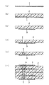
図1は、本実施形態における多層配線基板の製造方法をその工程順に示す断面図である。図1(a)において、銅箔等の金属箔1の両面に粗化処理を行う。粗化処理は、エッチング、機械研磨、金属溶射、型転写等により行われる。 FIG. 1 is a cross-sectional view showing a method of manufacturing a multilayer wiring board according to this embodiment in the order of steps. In FIG. 1A, a roughening process is performed on both surfaces of a metal foil 1 such as a copper foil. The roughening treatment is performed by etching, mechanical polishing, metal spraying, mold transfer, or the like.
次に、粗化処理された金属箔1と絶縁基材として熱可塑性樹脂フィルム2(本例では液晶ポリマー(LCP))とを熱融着や接着等により貼着し(図1(b))、金属箔1をエッチングすることにより、配線パターンを形成する(図1(c))。 Next, the roughened metal foil 1 and a thermoplastic resin film 2 (in this example, a liquid crystal polymer (LCP)) as an insulating base material are adhered by thermal fusion or adhesion (FIG. 1B). The metal foil 1 is etched to form a wiring pattern (FIG. 1C).
なお、熱可塑性樹脂フィルム2として、液晶ポリマー以外に、例えば、ポリエーテルエーテルケトン(PEEK)、ポリエーテルイミド(PEI)、ポリエーテルサルホン(PES)などのうち1つ又は複数からなる樹脂を用いてもよい。また、金属箔1は、銅以外に例えばアルミニウム、ニッケルなどの導電性を有するものであればよい。
As the
次に、図1(d)に示すように、図1(c)の熱可塑性樹脂フィルム2側から所定の位置に炭酸ガスレーザを照射して、有底ビアホール4を形成する。形成された有底ビアホール4は、炭酸ガスレーザの出力と照射時間を調整することにより、配線パターン3に穴を開けないようにしている。また、必要であれば有底ビアホール4の形成後、出来上がったビア底面をデスミア処理してもよい。
Next, as shown in FIG.1 (d), a carbon dioxide laser is irradiated to a predetermined position from the
レーザによる有底ビアホール4の形成には、炭酸ガスレーザ以外に固体レーザ(YAGレーザ、サファイアレーザなど)、気体レーザ(炭酸ガスレーザ、アルゴンイオンレーザ、ヘリウム−ネオンレーザなど)、半導体レーザ、色素レーザ、エキシマレーザ、自由電子レーザなどを用いてもよい。
The bottomed via
次に、図1(e)に示すように、基材に形成された有底ビアホール4に層間接続材料として導電性粒子5を充填する。導電性粒子5は、スクリーン印刷機等により、ビアホール4内に印刷充填する。ビアホール4内への導電性ペースト5の充填は、確実にできるのであれば、ディスペンサ等を用いる方法も可能である。
Next, as shown in FIG.1 (e), the bottomed via-
ここで、導電性粒子5は、配線パターンの表面を粗化処理して設けられた凹凸部の凹部に入り込まない大きさであり、また、配線材料よりも硬度が同等若しくは低い材料からなるものである。なお、導電性粒子5は、金、銀、銅、はんだなどや、これらの合金若しくは混合物であることが好ましい。
Here, the
本実施形態では、導電性粒子5のみとして説明するが、取り扱いを良くするために、有機溶剤及びバインダ樹脂をごく少量加えた導電性ペーストを使用してもよい。この場合、導電性ペースト充填後、加熱等により溶剤成分を蒸発乾燥させる。
In the present embodiment, the
有機溶剤は、ペースト化のために添加するものであり、バインダ樹脂は、金属配線に導電性粒子5を密着凝集させたり、導電性粒子5同士を凝集させ導電性を向上させるためのものである。しかし、バインダ樹脂自体は不導体であるので、バインダ樹脂は、加えないか、加えてもごく少量であることが望ましい。導電性ペースト内に必要以上のバインダ樹脂が含まれていると、接触部に不要な樹脂が入り込んでしまい、接続安定性を確保することができないからである。なお、バインダ樹脂は、弾性率や熱膨張率が同じであれば好ましく、基材と同じ樹脂の他、ポリエステル、ポリアミド、ポリカーボネート、ポリビニルブチラールなどが用いられる。
The organic solvent is added for pasting, and the binder resin is used to improve the conductivity by agglomerating the
次に、図1(f)に示すように、図1(e)の単一配線基板を複数枚重ねて、上下両面から真空熱プレス機により一括積層して多層配線基板を形成する。本例では、例えば280〜320℃の温度に加熱し0.5〜5MPaの圧力で加圧する。これにより、各単一配線基板の熱可塑性樹脂フィルム2は熱融着して一体化するとともに、導電性粒子5により層間接続が行われる。
Next, as shown in FIG. 1 (f), a plurality of the single wiring boards of FIG. 1 (e) are stacked and stacked together from above and below by a vacuum hot press to form a multilayer wiring board. In this example, it heats to the temperature of 280-320 degreeC, for example, and pressurizes with the pressure of 0.5-5 Mpa. Thereby, the
このような製造方法によれば、各単一配線基板が熱可塑性樹脂フィルム2で形成されているので、加熱により熱可塑性樹脂フィルム2が軟化し、加圧により各単一配線基板が確実に接続される。
According to such a manufacturing method, since each single wiring board is formed of the
また、導電性粒子5は、配線パターン3の表面を粗化処理して設けられた凹凸部の凹部に入り込まない大きさであり、また、配線材料よりも硬度が同等若しくは低い材料からなるものであることにより、真空熱プレス機により一括積層させる際、導電性粒子5に配線の凸部が挿入若しくは凸部が導電性粒子5に包まれるので比較的低い圧力で安定した導通を得ることができる。
The
なお、一般にビア底面となる金属箔1の熱可塑性樹脂フィルム2との接着面側は、ピール強度確保のために粗化処理されているので、ビア底面を粗化処理しなくてもよい。したがって、そのような場合には、金属箔1と熱可塑性フィルム2を接着させ、配線パターン3が形成された後、配線パターンの表面を粗化処理すればよい。
In general, the adhesive surface side of the metal foil 1 that becomes the via bottom surface with the
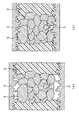
次に、図1(f)の一括積層における層間接続について、図2を用いて説明する。図2は、図1(f)に示す層間接続部Aにおけるビアホール内の状態を模式的に示す断面図である。 Next, interlayer connection in the collective stacking of FIG. 1 (f) will be described with reference to FIG. FIG. 2 is a cross-sectional view schematically showing a state in the via hole in the interlayer connection portion A shown in FIG.
図2(a)において、有底ビアホール4の底部となる配線パターン3の表面は粗化処理され凹凸部が形成されており、有底ビアホール4には導電性粒子5が充填されている。ここで、導電性粒子5は粗化処理された配線パターン3表面の凹凸部の凹部に入り込まない大きさを有する。また、導電性粒子5は、配線材料よりも硬度が同等若しくは低いものを選択することが好ましい。本例においては、配線材料は銅であり、導電性粒子5にはそれよりも硬度の低い銀粒子が充填されている。なお、導電性粒子5は、配線となる金属箔1より硬度が低い材料からなるものであればよく、銅箔であれば金、銀、鉛、亜鉛やこれらを混合するなどした粒子であってもよい。
In FIG. 2A, the surface of the
導電性粒子5は、配線表面の表面粗さを測定することにより、配線表面の凹凸部の凹部に入り込まない大きさとしてもよい。また、導電性粒子5の大きさに合わせて配線表面の凹凸部の凹部を形成するようにしてもよい。
The
真空熱プレス機により行われた多層配線基板の層間接続部の接続状態は、図2(b)に示すようである。銅配線の凹凸部の凸部が銀粒子に挿入され新生面が生じると同時に、銀粒子に銅配線の凸部の一部が包み込まれアンカー効果が生じる。また、導通した後、銅配線と銀粒子との接点付近の隙間及び銀粒子同士の隙間に基材樹脂が流動することにより、接点間の凝集力を得ている。 The connection state of the interlayer connection portion of the multilayer wiring board performed by the vacuum heat press is as shown in FIG. The convex part of the concavo-convex part of the copper wiring is inserted into the silver particles and a new surface is generated. Moreover, after conduction | electrical_connection, the base resin flows into the clearance gap between the contact of copper wiring and silver particle, and the clearance gap between silver particles, and the cohesion force between contacts is acquired.
このように、導電性粒子5を配線表面の凹凸部の凹部に入り込まない大きさとすることにより、配線表面の凸部と導電性粒子5とが点接触や線接触し、真空熱プレス時の圧力が低くても容易に導通させることができる。
Thus, by setting the
また、導電性粒子5の硬度が配線材料よりも同等若しくは低い材料からなることにより、凸部が粒子に突き刺さり新生面が生じると同時に、導電性粒子5に凸部の一部が包み込まれアンカー効果が生じるため、接続の安定性を上げることができる。
Further, since the
また、配線表面の凹凸部と導電性粒子5との接触及び導電性粒子5同士の接触の後に、基材樹脂が接点付近の隙間に流動するので、不要な樹脂が入り込まず、抵抗値も低く抑えることができる。
In addition, since the base resin flows into the gaps near the contacts after the contact between the
このように、配線表面の凹凸部と導電性粒子5との接触部や導電性粒子5同士の凝集力を強めるため、導通させた後、さらにプレスを続け、配線と導電性粒子5との接点付近の隙間に基材樹脂を流動させることにより、接点間の凝集力を得ることができ、より高い層間接続信頼性を確保することが可能となる。
Thus, in order to strengthen the contact part of the uneven | corrugated | grooved part of the wiring surface and the
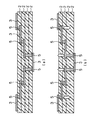
また、比較的低い圧力でも積層させることができるため、図3(a)のような積層パターンでも問題なく製造することができる。ここで、配線パターン3表面が粗化処理されておらず、導電性粒子5の大きさや硬度が制御されていない場合、真空熱プレス時に高い圧力が必要となり、軟化した熱可塑性樹脂よりも層間接続部の方が硬いため、図3(b)に示すように配線が傾いてしまう。
Further, since lamination can be performed even at a relatively low pressure, the lamination pattern as shown in FIG. 3A can be produced without any problem. Here, when the surface of the
以上のように本実施形態における多層配線基板の製造方法によれば、絶縁基材に熱可塑性樹脂フィルム2を用い、その基材に形成された配線パターン3表面を粗化処理し、導電性粒子5の大きさを粗化処理された凹凸部の凹部に入り込まない大きさとし、且つ、硬度を配線パターン3の材料よりも同等若しくは低いものとすることにより、比較的低い圧力で信頼性が高い多層配線基板を製造することができる。
As described above, according to the method for manufacturing a multilayer wiring board in the present embodiment, the surface of the
また、導電性粒子5は、配線パターン3の表面に設けられた凹凸部の凹部に入り込まない大きさであり、また、配線材料よりも硬度が同等若しくは低い材料からなるものとすることにより、配線の凹凸部の凸部が導電性粒子5に挿入され新生面が生じると同時に、配線の凸部の一部が導電性粒子5に包み込まれ、安定した導通を確保することができる。
In addition, the
また、導電性粒子5と配線の凹凸部との間、及び導電性粒子間に基材樹脂をバインディングさせることにより、凝集力が増し、高い接続信頼性を確保することができる。
In addition, by binding the base resin between the
1 金属箔、 2 熱可塑性樹脂フィルム、 3 配線パターン、 4 有底ビアホール、 5 導電性粒子 DESCRIPTION OF SYMBOLS 1 Metal foil, 2 Thermoplastic resin film, 3 Wiring pattern, 4 Bottomed via hole, 5 Conductive particle
Claims (10)
上記配線パターンには、表面に凹凸部が形成されており、
上記層間接続部には、導電性粒子が充填されていることを特徴とする多層配線基板。 A plurality of single wiring boards provided with wiring patterns and interlayer connection portions are laminated on an insulating base material made of a thermoplastic resin, and the other is obtained by heating and pressing the plurality of single wiring boards. In a multilayer wiring board formed by fusing with a single wiring board,
The wiring pattern has an uneven portion on the surface,
A multilayer wiring board, wherein the interlayer connection portion is filled with conductive particles.
表面に凹凸部を有する配線パターンを形成する工程と、
上記配線パターンの反対側から基板の厚み方向に配線パターンに達する有底ビアホールを形成する工程と、
上記有底ビアホールに導電性粒子を充填して単一配線板を作製する工程と、
複数の該単一配線基板を加熱加圧することにより他の単一配線基板と融着させる工程と
を有することを特徴とする多層配線基板の製造方法。 In a manufacturing method of a multilayer wiring board formed by laminating a plurality of single wiring boards provided with wiring patterns and interlayer connection portions on an insulating base material made of thermoplastic resin,
Forming a wiring pattern having an uneven portion on the surface;
Forming a bottomed via hole reaching the wiring pattern in the thickness direction of the substrate from the opposite side of the wiring pattern;
Filling the bottomed via hole with conductive particles to produce a single wiring board;
And a step of fusing the single wiring board to another single wiring board by heating and pressurizing the plurality of single wiring boards.
上記絶縁基材と金属箔とを接着する工程と、
上記絶縁基材に接着された金属箔に上記配線パターンを形成する工程と、
上記金属箔に形成された配線パターンの表面を粗化処理して凹凸部を形成する工程と
を有することを特徴とする請求項6記載の多層配線基板の製造方法。 The step of forming a wiring pattern having an uneven portion on the surface,
Bonding the insulating base and the metal foil;
Forming the wiring pattern on the metal foil adhered to the insulating substrate;
The method of manufacturing a multilayer wiring board according to claim 6, further comprising: roughening a surface of the wiring pattern formed on the metal foil to form an uneven portion.
金属箔の表面を粗化処理して凹凸部を形成する工程と、
上記凹凸部が形成された金属箔と上記絶縁基材とを接着する工程と、
上記凹凸部が形成された金属箔に上記配線パターンを形成する工程と
を有することを特徴とする請求項6記載の多層配線基板の製造方法。 The step of forming the wiring pattern having the uneven portion includes
A step of roughening the surface of the metal foil to form an uneven portion;
Adhering the metal foil on which the irregularities are formed and the insulating substrate;
The method for producing a multilayer wiring board according to claim 6, further comprising: forming the wiring pattern on the metal foil on which the uneven portion is formed.
7. The method for manufacturing a multilayer wiring board according to claim 6, wherein the conductive particles are made of a material having a hardness equal to or lower than that of the material of the wiring pattern.
Priority Applications (1)
| Application Number | Priority Date | Filing Date | Title |
|---|---|---|---|
| JP2003363712A JP2005129727A (en) | 2003-10-23 | 2003-10-23 | Multilayer wiring board and manufacturing method thereof |
Applications Claiming Priority (1)
| Application Number | Priority Date | Filing Date | Title |
|---|---|---|---|
| JP2003363712A JP2005129727A (en) | 2003-10-23 | 2003-10-23 | Multilayer wiring board and manufacturing method thereof |
Publications (1)
| Publication Number | Publication Date |
|---|---|
| JP2005129727A true JP2005129727A (en) | 2005-05-19 |
Family
ID=34642952
Family Applications (1)
| Application Number | Title | Priority Date | Filing Date |
|---|---|---|---|
| JP2003363712A Pending JP2005129727A (en) | 2003-10-23 | 2003-10-23 | Multilayer wiring board and manufacturing method thereof |
Country Status (1)
| Country | Link |
|---|---|
| JP (1) | JP2005129727A (en) |
Cited By (4)
| Publication number | Priority date | Publication date | Assignee | Title |
|---|---|---|---|---|
| JP2007042696A (en) * | 2005-08-01 | 2007-02-15 | Furukawa Circuit Foil Kk | Multilayer circuit board |
| JP2007042695A (en) * | 2005-08-01 | 2007-02-15 | Furukawa Circuit Foil Kk | Multilayer circuit board |
| JP2008103376A (en) * | 2006-10-17 | 2008-05-01 | Hitachi Cable Ltd | Multilayer printed wiring board and manufacturing method thereof |
| US8963017B2 (en) | 2011-08-31 | 2015-02-24 | Denso Corporation | Multilayer board |
-
2003
- 2003-10-23 JP JP2003363712A patent/JP2005129727A/en active Pending
Cited By (4)
| Publication number | Priority date | Publication date | Assignee | Title |
|---|---|---|---|---|
| JP2007042696A (en) * | 2005-08-01 | 2007-02-15 | Furukawa Circuit Foil Kk | Multilayer circuit board |
| JP2007042695A (en) * | 2005-08-01 | 2007-02-15 | Furukawa Circuit Foil Kk | Multilayer circuit board |
| JP2008103376A (en) * | 2006-10-17 | 2008-05-01 | Hitachi Cable Ltd | Multilayer printed wiring board and manufacturing method thereof |
| US8963017B2 (en) | 2011-08-31 | 2015-02-24 | Denso Corporation | Multilayer board |
Similar Documents
| Publication | Publication Date | Title |
|---|---|---|
| JP3969192B2 (en) | Manufacturing method of multilayer wiring board | |
| JP2006073763A (en) | Multilayer substrate manufacturing method | |
| US6768061B2 (en) | Multilayer circuit board | |
| JP3867593B2 (en) | Printed circuit board manufacturing method and printed circuit board formed by the manufacturing method | |
| JP2012079994A (en) | Component built-in printed circuit board and its manufacturing method | |
| US20080149374A1 (en) | Laminated multi-layer circuit board | |
| JP3882540B2 (en) | Printed circuit board manufacturing method and printed circuit board formed by the manufacturing method | |
| JPH09283881A (en) | Interlayer connection structure on circuit board | |
| WO2007114111A1 (en) | Multilayer wiring board and its manufacturing method | |
| JP2007324550A (en) | Multilayer board | |
| CN100544556C (en) | Multilayer printed circuit board and manufacture method thereof | |
| JP2006093439A (en) | Multilayer substrate and manufacturing method thereof | |
| CN103796418B (en) | A kind of circuit board and the manufacture method of circuit board | |
| JP4508859B2 (en) | Manufacturing method of semiconductor substrate | |
| JP2004087944A (en) | Manufacturing method of substrate with logo mark | |
| JP2006049536A (en) | Multilayer circuit board | |
| JP2000294931A (en) | Multilayer wiring board and method of manufacturing the same | |
| JP2010021369A (en) | Wiring board with built-in component and manufacturing method thereof | |
| JP2004172533A (en) | Printed circuit board manufacturing method and printed circuit board formed by the manufacturing method | |
| JP2007115952A (en) | Interposer substrate and manufacturing method thereof | |
| JP4821276B2 (en) | Multilayer printed wiring board manufacturing method and multilayer printed wiring board | |
| JP2005129725A (en) | Multilayer wiring board and manufacturing method thereof | |
| JP4003593B2 (en) | Multilayer printed circuit board | |
| JP2009158641A (en) | Method of producing module with built-in component | |
| JP4797742B2 (en) | Multilayer wiring board and manufacturing method thereof |
Legal Events
| Date | Code | Title | Description |
|---|---|---|---|
| A621 | Written request for application examination |
Effective date: 20061006 Free format text: JAPANESE INTERMEDIATE CODE: A621 |
|
| A977 | Report on retrieval |
Effective date: 20090224 Free format text: JAPANESE INTERMEDIATE CODE: A971007 |
|
| A131 | Notification of reasons for refusal |
Effective date: 20090407 Free format text: JAPANESE INTERMEDIATE CODE: A131 |
|
| A02 | Decision of refusal |
Free format text: JAPANESE INTERMEDIATE CODE: A02 Effective date: 20090804 |