JP2005129902A - 半導体装置およびその製造方法 - Google Patents
半導体装置およびその製造方法 Download PDFInfo
- Publication number
- JP2005129902A JP2005129902A JP2004259357A JP2004259357A JP2005129902A JP 2005129902 A JP2005129902 A JP 2005129902A JP 2004259357 A JP2004259357 A JP 2004259357A JP 2004259357 A JP2004259357 A JP 2004259357A JP 2005129902 A JP2005129902 A JP 2005129902A
- Authority
- JP
- Japan
- Prior art keywords
- insulating film
- film
- semiconductor device
- barrier metal
- interlayer insulating
- Prior art date
- Legal status (The legal status is an assumption and is not a legal conclusion. Google has not performed a legal analysis and makes no representation as to the accuracy of the status listed.)
- Granted
Links
Images


Classifications
-
- H—ELECTRICITY
- H10—SEMICONDUCTOR DEVICES; ELECTRIC SOLID-STATE DEVICES NOT OTHERWISE PROVIDED FOR
- H10W—GENERIC PACKAGES, INTERCONNECTIONS, CONNECTORS OR OTHER CONSTRUCTIONAL DETAILS OF DEVICES COVERED BY CLASS H10
- H10W20/00—Interconnections in chips, wafers or substrates
- H10W20/01—Manufacture or treatment
- H10W20/031—Manufacture or treatment of conductive parts of the interconnections
- H10W20/056—Manufacture or treatment of conductive parts of the interconnections by filling conductive material into holes, grooves or trenches
-
- H—ELECTRICITY
- H10—SEMICONDUCTOR DEVICES; ELECTRIC SOLID-STATE DEVICES NOT OTHERWISE PROVIDED FOR
- H10W—GENERIC PACKAGES, INTERCONNECTIONS, CONNECTORS OR OTHER CONSTRUCTIONAL DETAILS OF DEVICES COVERED BY CLASS H10
- H10W20/00—Interconnections in chips, wafers or substrates
- H10W20/01—Manufacture or treatment
- H10W20/071—Manufacture or treatment of dielectric parts thereof
- H10W20/074—Manufacture or treatment of dielectric parts thereof of dielectric parts comprising thin functional dielectric layers, e.g. dielectric etch-stop, barrier, capping or liner layers
-
- H—ELECTRICITY
- H10—SEMICONDUCTOR DEVICES; ELECTRIC SOLID-STATE DEVICES NOT OTHERWISE PROVIDED FOR
- H10W—GENERIC PACKAGES, INTERCONNECTIONS, CONNECTORS OR OTHER CONSTRUCTIONAL DETAILS OF DEVICES COVERED BY CLASS H10
- H10W20/00—Interconnections in chips, wafers or substrates
- H10W20/01—Manufacture or treatment
- H10W20/071—Manufacture or treatment of dielectric parts thereof
- H10W20/074—Manufacture or treatment of dielectric parts thereof of dielectric parts comprising thin functional dielectric layers, e.g. dielectric etch-stop, barrier, capping or liner layers
- H10W20/075—Manufacture or treatment of dielectric parts thereof of dielectric parts comprising thin functional dielectric layers, e.g. dielectric etch-stop, barrier, capping or liner layers of multilayered thin functional dielectric layers
-
- H—ELECTRICITY
- H10—SEMICONDUCTOR DEVICES; ELECTRIC SOLID-STATE DEVICES NOT OTHERWISE PROVIDED FOR
- H10W—GENERIC PACKAGES, INTERCONNECTIONS, CONNECTORS OR OTHER CONSTRUCTIONAL DETAILS OF DEVICES COVERED BY CLASS H10
- H10W20/00—Interconnections in chips, wafers or substrates
- H10W20/01—Manufacture or treatment
- H10W20/071—Manufacture or treatment of dielectric parts thereof
- H10W20/074—Manufacture or treatment of dielectric parts thereof of dielectric parts comprising thin functional dielectric layers, e.g. dielectric etch-stop, barrier, capping or liner layers
- H10W20/077—Manufacture or treatment of dielectric parts thereof of dielectric parts comprising thin functional dielectric layers, e.g. dielectric etch-stop, barrier, capping or liner layers on sidewalls or on top surfaces of conductors
-
- H—ELECTRICITY
- H10—SEMICONDUCTOR DEVICES; ELECTRIC SOLID-STATE DEVICES NOT OTHERWISE PROVIDED FOR
- H10W—GENERIC PACKAGES, INTERCONNECTIONS, CONNECTORS OR OTHER CONSTRUCTIONAL DETAILS OF DEVICES COVERED BY CLASS H10
- H10W20/00—Interconnections in chips, wafers or substrates
- H10W20/01—Manufacture or treatment
- H10W20/071—Manufacture or treatment of dielectric parts thereof
- H10W20/093—Manufacture or treatment of dielectric parts thereof by modifying materials of the dielectric parts
- H10W20/095—Manufacture or treatment of dielectric parts thereof by modifying materials of the dielectric parts by irradiating with electromagnetic or particle radiation
-
- H—ELECTRICITY
- H10—SEMICONDUCTOR DEVICES; ELECTRIC SOLID-STATE DEVICES NOT OTHERWISE PROVIDED FOR
- H10W—GENERIC PACKAGES, INTERCONNECTIONS, CONNECTORS OR OTHER CONSTRUCTIONAL DETAILS OF DEVICES COVERED BY CLASS H10
- H10W20/00—Interconnections in chips, wafers or substrates
- H10W20/01—Manufacture or treatment
- H10W20/071—Manufacture or treatment of dielectric parts thereof
- H10W20/093—Manufacture or treatment of dielectric parts thereof by modifying materials of the dielectric parts
- H10W20/096—Manufacture or treatment of dielectric parts thereof by modifying materials of the dielectric parts by contacting with gases, liquids or plasmas
-
- H—ELECTRICITY
- H10—SEMICONDUCTOR DEVICES; ELECTRIC SOLID-STATE DEVICES NOT OTHERWISE PROVIDED FOR
- H10W—GENERIC PACKAGES, INTERCONNECTIONS, CONNECTORS OR OTHER CONSTRUCTIONAL DETAILS OF DEVICES COVERED BY CLASS H10
- H10W20/00—Interconnections in chips, wafers or substrates
- H10W20/40—Interconnections external to wafers or substrates, e.g. back-end-of-line [BEOL] metallisations or vias connecting to gate electrodes
- H10W20/41—Interconnections external to wafers or substrates, e.g. back-end-of-line [BEOL] metallisations or vias connecting to gate electrodes characterised by their conductive parts
- H10W20/425—Barrier, adhesion or liner layers
-
- H—ELECTRICITY
- H10—SEMICONDUCTOR DEVICES; ELECTRIC SOLID-STATE DEVICES NOT OTHERWISE PROVIDED FOR
- H10W—GENERIC PACKAGES, INTERCONNECTIONS, CONNECTORS OR OTHER CONSTRUCTIONAL DETAILS OF DEVICES COVERED BY CLASS H10
- H10W20/00—Interconnections in chips, wafers or substrates
- H10W20/01—Manufacture or treatment
- H10W20/031—Manufacture or treatment of conductive parts of the interconnections
- H10W20/063—Manufacture or treatment of conductive parts of the interconnections by forming conductive members before forming protective insulating material
-
- H—ELECTRICITY
- H10—SEMICONDUCTOR DEVICES; ELECTRIC SOLID-STATE DEVICES NOT OTHERWISE PROVIDED FOR
- H10W—GENERIC PACKAGES, INTERCONNECTIONS, CONNECTORS OR OTHER CONSTRUCTIONAL DETAILS OF DEVICES COVERED BY CLASS H10
- H10W20/00—Interconnections in chips, wafers or substrates
- H10W20/01—Manufacture or treatment
- H10W20/071—Manufacture or treatment of dielectric parts thereof
- H10W20/081—Manufacture or treatment of dielectric parts thereof by forming openings in the dielectric parts
- H10W20/084—Manufacture or treatment of dielectric parts thereof by forming openings in the dielectric parts for dual-damascene structures
Landscapes
- Internal Circuitry In Semiconductor Integrated Circuit Devices (AREA)
- Weting (AREA)
Abstract
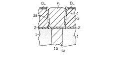
【解決手段】トレンチ溝3aに埋設された導体膜5を、その上面が、バリアメタル膜4との接触部において、第2の層間絶縁膜3の上面よりも下方に位置する態様で形成された構造とする。またその製造に際しては、CMPによる研磨処理の後に、非窒化性雰囲気でプラズマ処理を行い、第2の層間絶縁膜3の上層部および導体膜5の上層部にダメージ層を形成する。そして、該ダメージ層の一部をエッチングにより除去する。
【選択図】 図1
Description
いる。
(a)絶縁膜を成膜する。
(b)前記絶縁膜にトレンチ溝を形成する。
(c)前記トレンチ溝の内壁面にバリアメタル膜を成膜する。
(d)前記トレンチ溝を埋め込むかたちで、導体膜を前記バリアメタル膜に積層形成する。
(e)前記導体膜を研磨により除去して、前記絶縁膜を露出させる。
(f)非窒化性雰囲気で、前記露出させた絶縁膜の上層部および前記導体膜の上層部にダメージ層を形成する。
(g)前記ダメージ層の少なくとも一部をエッチングにより除去する。
といった各工程を備える。
図1に、本発明にかかる半導体装置についてその第1の実施の形態を示す。
(RF)電力を「470W」、基板温度を「350℃」、処理ガス種をTMS(トリメチルシラン)、HeおよびNH3とする。
を「350℃」、処理ガス種をTMS(トリメチルシラン)およびO2とする。
図9に、本発明にかかる半導体装置についてその第2の実施の形態を示す。
なお、上記各実施の形態は、以下の形態をもって実施することもできる。

Claims (11)
- トレンチ溝を有する絶縁膜と、前記トレンチ溝の内壁面に形成されたバリアメタル膜と、該バリアメタル膜を介して前記トレンチ溝に埋設されて形成されてなる導体膜とを有する半導体装置において、
前記導体膜は、その上面が、少なくとも前記バリアメタル膜との接触部において該バリアメタル膜の上端よりも下方に位置する態様で形成されてなることを特徴とする半導体装置。 - 前記導体膜は、その上面が、少なくとも前記バリアメタル膜との接触部において、前記絶縁膜の上面よりも下方に位置する態様で形成されてなることを特徴とする請求項1に記載の半導体装置。
- 前記絶縁膜は、その上面が、少なくとも前記バリアメタル膜との接触部において該バリアメタル膜の上端よりも下方に位置する態様で形成されてなることを特徴とする請求項1または2に記載の半導体装置。
- 前記導体膜は、その上面が、前記バリアメタル膜との接触部に近づくほど低下する略円弧形状の断面をもって形成されてなることを特徴とする請求項1〜3のいずれか一項に記載の半導体装置。
- 前記絶縁膜の上層部には、その組成が変化した層が存在してなることを特徴とする請求項1〜4のいずれか一項に記載の半導体装置。
- 前記絶縁膜が、酸化シリコンより誘電率が低い低誘電率材料であることを特徴とする請求項1〜5のいずれか1項に記載の半導体装置。
- 前記低誘電率材料が、メチル基を含有する酸化シリコン、ベンゾシクロブテン(BCB)、フッ素化酸化シリコン(SiOF)、ベンゾシクロブテン(BCB)、HSQ(ハイドロゲンシルセスキオキサン)、MSQ(メチルシルセスキオキサン)、HMSQ(ハイドライド−メチルシルセスキオキサン)、ポリイミド系ポリマー、アリレンエーテル系ポリマー、シクロブテン系ポリマー、パーフロロシクロブテン(PFCB)からなる群から選ばれることを特徴とする請求項6に記載の半導体装置。
- 前記低誘電率材料の比誘電率が2.7〜3であることを特徴とする請求項6に記載の半導体装置。
- 絶縁膜を成膜する工程と、
前記絶縁膜にトレンチ溝を形成する工程と、
前記トレンチ溝の内壁面にバリアメタル膜を成膜する工程と、
前記トレンチ溝を埋め込むかたちで、導体膜を前記バリアメタル膜に積層形成する工程と、
前記導体膜を研磨により除去して、前記絶縁膜を露出させる工程と、
非窒化性雰囲気で、前記露出させた絶縁膜の上層部および前記導体膜の上層部にダメージ層を形成する工程と、
前記ダメージ層の少なくとも一部をエッチングにより除去する工程と、
を備えることを特徴とする半導体装置の製造方法。 - 前記絶縁膜として、酸化シリコンより誘電率が低い低誘電率材料を用いることを特徴とする請求項9に記載の半導体装置の製造方法。
- 前記低誘電率材料が、メチル基を含有する酸化シリコン、ベンゾシクロブテン(BCB)、フッ素化酸化シリコン(SiOF)、ベンゾシクロブテン(BCB)、HSQ(ハイドロゲンシルセスキオキサン)、MSQ(メチルシルセスキオキサン)、HMSQ(ハイドライド−メチルシルセスキオキサン)、ポリイミド系ポリマー、アリレンエーテル系ポリマー、シクロブテン系ポリマー、パーフロロシクロブテン(PFCB)からなる群から選ばれることを特徴とする請求項10に記載の半導体装置の製造方法。
Priority Applications (3)
| Application Number | Priority Date | Filing Date | Title |
|---|---|---|---|
| JP2004259357A JP4266901B2 (ja) | 2003-09-30 | 2004-09-07 | 半導体装置およびその製造方法 |
| US10/950,689 US7273810B2 (en) | 2003-09-30 | 2004-09-28 | Semiconductor apparatus and method of fabricating the same |
| CNB2004100834796A CN100356562C (zh) | 2003-09-30 | 2004-09-30 | 半导体装置及其制造方法 |
Applications Claiming Priority (2)
| Application Number | Priority Date | Filing Date | Title |
|---|---|---|---|
| JP2003341597 | 2003-09-30 | ||
| JP2004259357A JP4266901B2 (ja) | 2003-09-30 | 2004-09-07 | 半導体装置およびその製造方法 |
Publications (2)
| Publication Number | Publication Date |
|---|---|
| JP2005129902A true JP2005129902A (ja) | 2005-05-19 |
| JP4266901B2 JP4266901B2 (ja) | 2009-05-27 |
Family
ID=34554702
Family Applications (1)
| Application Number | Title | Priority Date | Filing Date |
|---|---|---|---|
| JP2004259357A Expired - Fee Related JP4266901B2 (ja) | 2003-09-30 | 2004-09-07 | 半導体装置およびその製造方法 |
Country Status (3)
| Country | Link |
|---|---|
| US (1) | US7273810B2 (ja) |
| JP (1) | JP4266901B2 (ja) |
| CN (1) | CN100356562C (ja) |
Cited By (6)
| Publication number | Priority date | Publication date | Assignee | Title |
|---|---|---|---|---|
| WO2006126536A1 (ja) * | 2005-05-25 | 2006-11-30 | Nec Corporation | 半導体装置及びその製造方法 |
| JP2010507236A (ja) * | 2006-10-11 | 2010-03-04 | インターナショナル・ビジネス・マシーンズ・コーポレーション | 半導体デバイスおよび相互接続構造体の形成方法 |
| US8399954B2 (en) | 2006-03-17 | 2013-03-19 | Renesas Electronics Corporation | Semiconductor integrated circuit device |
| KR20140028376A (ko) * | 2012-08-28 | 2014-03-10 | 삼성전자주식회사 | 반도체 장치 및 그 제조 방법 |
| KR20220148065A (ko) * | 2021-04-28 | 2022-11-04 | 타이완 세미콘덕터 매뉴팩쳐링 컴퍼니 리미티드 | 반도체 디바이스를 위한 콘택트 및 그 형성 방법 |
| WO2024143209A1 (ja) * | 2022-12-28 | 2024-07-04 | 富士フイルム株式会社 | 積層体の製造方法、感光性樹脂組成物、及び、半導体部材の製造方法 |
Families Citing this family (10)
| Publication number | Priority date | Publication date | Assignee | Title |
|---|---|---|---|---|
| US20070072412A1 (en) * | 2005-09-27 | 2007-03-29 | International Business Machines Corporation | Preventing damage to interlevel dielectric |
| JP5081833B2 (ja) * | 2006-10-30 | 2012-11-28 | 三洋電機株式会社 | 静電動作装置 |
| KR101113327B1 (ko) * | 2009-12-29 | 2012-03-13 | 주식회사 하이닉스반도체 | 관통전극을 갖는 반도체소자 및 그 제조방법 |
| US8525339B2 (en) | 2011-07-27 | 2013-09-03 | International Business Machines Corporation | Hybrid copper interconnect structure and method of fabricating same |
| US9312203B2 (en) | 2013-01-02 | 2016-04-12 | Globalfoundries Inc. | Dual damascene structure with liner |
| JP2015053444A (ja) * | 2013-09-09 | 2015-03-19 | パナソニックIpマネジメント株式会社 | フレキシブル半導体装置およびその製造方法ならびに画像表示装置 |
| US9370854B2 (en) * | 2013-11-13 | 2016-06-21 | Taiwan Semiconductor Manufacturing Co., Ltd. | Method of fabricating a semiconductor device, and chemical mechanical polish tool |
| US10522754B2 (en) * | 2016-06-15 | 2019-12-31 | Crossbar, Inc. | Liner layer for dielectric block layer |
| US10749110B1 (en) | 2016-07-15 | 2020-08-18 | Crossbar, Inc. | Memory stack liner comprising dielectric block layer material |
| US11456242B2 (en) | 2020-07-21 | 2022-09-27 | Nanya Technology Corporation | Semiconductor device with stress-relieving structures and method for fabricating the same |
Family Cites Families (7)
| Publication number | Priority date | Publication date | Assignee | Title |
|---|---|---|---|---|
| JP3297220B2 (ja) * | 1993-10-29 | 2002-07-02 | 株式会社東芝 | 半導体装置の製造方法および半導体装置 |
| US5730835A (en) * | 1996-01-31 | 1998-03-24 | Micron Technology, Inc. | Facet etch for improved step coverage of integrated circuit contacts |
| TW478101B (en) * | 2000-03-23 | 2002-03-01 | Ibm | Structure for protecting copper interconnects in low dielectric constant materials from oxidation |
| JP4535629B2 (ja) | 2001-02-21 | 2010-09-01 | ルネサスエレクトロニクス株式会社 | 半導体装置の製造方法 |
| KR100531419B1 (ko) * | 2001-06-12 | 2005-11-28 | 주식회사 하이닉스반도체 | 반도체소자 및 그의 제조방법 |
| US7071515B2 (en) * | 2003-07-14 | 2006-07-04 | Taiwan Semiconductor Manufacturing Co., Ltd. | Narrow width effect improvement with photoresist plug process and STI corner ion implantation |
| US6972253B2 (en) * | 2003-09-09 | 2005-12-06 | Taiwan Semiconductor Manufacturing Company, Ltd. | Method for forming dielectric barrier layer in damascene structure |
-
2004
- 2004-09-07 JP JP2004259357A patent/JP4266901B2/ja not_active Expired - Fee Related
- 2004-09-28 US US10/950,689 patent/US7273810B2/en not_active Expired - Lifetime
- 2004-09-30 CN CNB2004100834796A patent/CN100356562C/zh not_active Expired - Fee Related
Cited By (10)
| Publication number | Priority date | Publication date | Assignee | Title |
|---|---|---|---|---|
| WO2006126536A1 (ja) * | 2005-05-25 | 2006-11-30 | Nec Corporation | 半導体装置及びその製造方法 |
| JPWO2006126536A1 (ja) * | 2005-05-25 | 2008-12-25 | 日本電気株式会社 | 半導体装置及びその製造方法 |
| US8399954B2 (en) | 2006-03-17 | 2013-03-19 | Renesas Electronics Corporation | Semiconductor integrated circuit device |
| JP2010507236A (ja) * | 2006-10-11 | 2010-03-04 | インターナショナル・ビジネス・マシーンズ・コーポレーション | 半導体デバイスおよび相互接続構造体の形成方法 |
| KR20140028376A (ko) * | 2012-08-28 | 2014-03-10 | 삼성전자주식회사 | 반도체 장치 및 그 제조 방법 |
| KR101994237B1 (ko) * | 2012-08-28 | 2019-06-28 | 삼성전자 주식회사 | 반도체 장치 및 그 제조 방법 |
| KR20220148065A (ko) * | 2021-04-28 | 2022-11-04 | 타이완 세미콘덕터 매뉴팩쳐링 컴퍼니 리미티드 | 반도체 디바이스를 위한 콘택트 및 그 형성 방법 |
| US11961893B2 (en) | 2021-04-28 | 2024-04-16 | Taiwan Semiconductor Manufacturing Co., Ltd. | Contacts for semiconductor devices and methods of forming the same |
| KR102863364B1 (ko) * | 2021-04-28 | 2025-09-22 | 타이완 세미콘덕터 매뉴팩쳐링 컴퍼니 리미티드 | 반도체 디바이스를 위한 콘택트 및 그 형성 방법 |
| WO2024143209A1 (ja) * | 2022-12-28 | 2024-07-04 | 富士フイルム株式会社 | 積層体の製造方法、感光性樹脂組成物、及び、半導体部材の製造方法 |
Also Published As
| Publication number | Publication date |
|---|---|
| US7273810B2 (en) | 2007-09-25 |
| CN1612336A (zh) | 2005-05-04 |
| US20050093156A1 (en) | 2005-05-05 |
| CN100356562C (zh) | 2007-12-19 |
| JP4266901B2 (ja) | 2009-05-27 |
Similar Documents
| Publication | Publication Date | Title |
|---|---|---|
| US6432811B1 (en) | Method of forming structural reinforcement of highly porous low k dielectric films by Cu diffusion barrier structures | |
| JP4266901B2 (ja) | 半導体装置およびその製造方法 | |
| US8629560B2 (en) | Self aligned air-gap in interconnect structures | |
| CN100576494C (zh) | 利用保护性通路盖层形成半导体器件的双镶嵌布线的方法 | |
| US7514354B2 (en) | Methods for forming damascene wiring structures having line and plug conductors formed from different materials | |
| US20070178713A1 (en) | Method for forming a dielectric layer with an air gap, and a structure including the dielectric layer with the air gap | |
| US7348672B2 (en) | Interconnects with improved reliability | |
| CN113113350A (zh) | 半导体装置的形成方法 | |
| US6984581B2 (en) | Structural reinforcement of highly porous low k dielectric films by ILD posts | |
| US7781335B2 (en) | Method for fabricating semiconductor device | |
| WO2007091574A1 (ja) | 多層配線構造および多層配線の製造方法 | |
| US20120168957A1 (en) | Method to reduce depth delta between dense and wide features in dual damascene structures | |
| US20060151887A1 (en) | Interconnection structure having double diffusion barrier layer and method of fabricating the same | |
| JP4527948B2 (ja) | 半導体装置およびその製造方法 | |
| JP2005032875A (ja) | 半導体装置及びその製造方法 | |
| CN100378953C (zh) | 在层间介质互连中形成低电阻和可靠过孔的方法 | |
| CN101335256B (zh) | Nor闪存装置及制造该装置的方法 | |
| JP2004014828A (ja) | 半導体装置の製造方法 | |
| US6825561B1 (en) | Structure and method for eliminating time dependent dielectric breakdown failure of low-k material | |
| KR100709161B1 (ko) | 반도체 장치의 제조 방법 | |
| JP2011009642A (ja) | 半導体装置及びその製造方法 | |
| JP2011171432A (ja) | 半導体装置およびその製造方法 | |
| JP2004179424A (ja) | 半導体集積回路装置の製造方法 | |
| JP2004296620A (ja) | 半導体装置の製造方法 | |
| JP4967207B2 (ja) | 半導体装置の製造方法 |
Legal Events
| Date | Code | Title | Description |
|---|---|---|---|
| RD01 | Notification of change of attorney |
Free format text: JAPANESE INTERMEDIATE CODE: A7421 Effective date: 20051227 |
|
| A621 | Written request for application examination |
Free format text: JAPANESE INTERMEDIATE CODE: A621 Effective date: 20061012 |
|
| A131 | Notification of reasons for refusal |
Free format text: JAPANESE INTERMEDIATE CODE: A131 Effective date: 20081125 |
|
| A977 | Report on retrieval |
Free format text: JAPANESE INTERMEDIATE CODE: A971007 Effective date: 20081127 |
|
| A521 | Request for written amendment filed |
Free format text: JAPANESE INTERMEDIATE CODE: A523 Effective date: 20081222 |
|
| TRDD | Decision of grant or rejection written | ||
| A01 | Written decision to grant a patent or to grant a registration (utility model) |
Free format text: JAPANESE INTERMEDIATE CODE: A01 Effective date: 20090120 |
|
| A01 | Written decision to grant a patent or to grant a registration (utility model) |
Free format text: JAPANESE INTERMEDIATE CODE: A01 |
|
| A61 | First payment of annual fees (during grant procedure) |
Free format text: JAPANESE INTERMEDIATE CODE: A61 Effective date: 20090217 |
|
| FPAY | Renewal fee payment (event date is renewal date of database) |
Free format text: PAYMENT UNTIL: 20120227 Year of fee payment: 3 |
|
| FPAY | Renewal fee payment (event date is renewal date of database) |
Free format text: PAYMENT UNTIL: 20120227 Year of fee payment: 3 |
|
| FPAY | Renewal fee payment (event date is renewal date of database) |
Free format text: PAYMENT UNTIL: 20130227 Year of fee payment: 4 |
|
| LAPS | Cancellation because of no payment of annual fees |