JP2005140976A - 表示装置 - Google Patents
表示装置 Download PDFInfo
- Publication number
- JP2005140976A JP2005140976A JP2003377069A JP2003377069A JP2005140976A JP 2005140976 A JP2005140976 A JP 2005140976A JP 2003377069 A JP2003377069 A JP 2003377069A JP 2003377069 A JP2003377069 A JP 2003377069A JP 2005140976 A JP2005140976 A JP 2005140976A
- Authority
- JP
- Japan
- Prior art keywords
- layer
- resin
- substrate
- display device
- inorganic barrier
- Prior art date
- Legal status (The legal status is an assumption and is not a legal conclusion. Google has not performed a legal analysis and makes no representation as to the accuracy of the status listed.)
- Granted
Links
Images




Classifications
-
- G—PHYSICS
- G02—OPTICS
- G02F—OPTICAL DEVICES OR ARRANGEMENTS FOR THE CONTROL OF LIGHT BY MODIFICATION OF THE OPTICAL PROPERTIES OF THE MEDIA OF THE ELEMENTS INVOLVED THEREIN; NON-LINEAR OPTICS; FREQUENCY-CHANGING OF LIGHT; OPTICAL LOGIC ELEMENTS; OPTICAL ANALOGUE/DIGITAL CONVERTERS
- G02F1/00—Devices or arrangements for the control of the intensity, colour, phase, polarisation or direction of light arriving from an independent light source, e.g. switching, gating or modulating; Non-linear optics
- G02F1/01—Devices or arrangements for the control of the intensity, colour, phase, polarisation or direction of light arriving from an independent light source, e.g. switching, gating or modulating; Non-linear optics for the control of the intensity, phase, polarisation or colour
- G02F1/13—Devices or arrangements for the control of the intensity, colour, phase, polarisation or direction of light arriving from an independent light source, e.g. switching, gating or modulating; Non-linear optics for the control of the intensity, phase, polarisation or colour based on liquid crystals, e.g. single liquid crystal display cells
- G02F1/133—Constructional arrangements; Operation of liquid crystal cells; Circuit arrangements
- G02F1/1333—Constructional arrangements; Manufacturing methods
- G02F1/133305—Flexible substrates, e.g. plastics, organic film
-
- H—ELECTRICITY
- H10—SEMICONDUCTOR DEVICES; ELECTRIC SOLID-STATE DEVICES NOT OTHERWISE PROVIDED FOR
- H10K—ORGANIC ELECTRIC SOLID-STATE DEVICES
- H10K50/00—Organic light-emitting devices
- H10K50/80—Constructional details
- H10K50/84—Passivation; Containers; Encapsulations
- H10K50/844—Encapsulations
-
- H—ELECTRICITY
- H10—SEMICONDUCTOR DEVICES; ELECTRIC SOLID-STATE DEVICES NOT OTHERWISE PROVIDED FOR
- H10K—ORGANIC ELECTRIC SOLID-STATE DEVICES
- H10K59/00—Integrated devices, or assemblies of multiple devices, comprising at least one organic light-emitting element covered by group H10K50/00
- H10K59/80—Constructional details
- H10K59/87—Passivation; Containers; Encapsulations
- H10K59/873—Encapsulations
-
- H—ELECTRICITY
- H10—SEMICONDUCTOR DEVICES; ELECTRIC SOLID-STATE DEVICES NOT OTHERWISE PROVIDED FOR
- H10K—ORGANIC ELECTRIC SOLID-STATE DEVICES
- H10K77/00—Constructional details of devices covered by this subclass and not covered by groups H10K10/80, H10K30/80, H10K50/80 or H10K59/80
- H10K77/10—Substrates, e.g. flexible substrates
-
- C—CHEMISTRY; METALLURGY
- C09—DYES; PAINTS; POLISHES; NATURAL RESINS; ADHESIVES; COMPOSITIONS NOT OTHERWISE PROVIDED FOR; APPLICATIONS OF MATERIALS NOT OTHERWISE PROVIDED FOR
- C09K—MATERIALS FOR MISCELLANEOUS APPLICATIONS, NOT PROVIDED FOR ELSEWHERE
- C09K2323/00—Functional layers of liquid crystal optical display excluding electroactive liquid crystal layer characterised by chemical composition
- C09K2323/05—Bonding or intermediate layer characterised by chemical composition, e.g. sealant or spacer
- C09K2323/051—Inorganic, e.g. glass or silicon oxide
-
- C—CHEMISTRY; METALLURGY
- C09—DYES; PAINTS; POLISHES; NATURAL RESINS; ADHESIVES; COMPOSITIONS NOT OTHERWISE PROVIDED FOR; APPLICATIONS OF MATERIALS NOT OTHERWISE PROVIDED FOR
- C09K—MATERIALS FOR MISCELLANEOUS APPLICATIONS, NOT PROVIDED FOR ELSEWHERE
- C09K2323/00—Functional layers of liquid crystal optical display excluding electroactive liquid crystal layer characterised by chemical composition
- C09K2323/06—Substrate layer characterised by chemical composition
-
- H—ELECTRICITY
- H10—SEMICONDUCTOR DEVICES; ELECTRIC SOLID-STATE DEVICES NOT OTHERWISE PROVIDED FOR
- H10K—ORGANIC ELECTRIC SOLID-STATE DEVICES
- H10K59/00—Integrated devices, or assemblies of multiple devices, comprising at least one organic light-emitting element covered by group H10K50/00
-
- Y—GENERAL TAGGING OF NEW TECHNOLOGICAL DEVELOPMENTS; GENERAL TAGGING OF CROSS-SECTIONAL TECHNOLOGIES SPANNING OVER SEVERAL SECTIONS OF THE IPC; TECHNICAL SUBJECTS COVERED BY FORMER USPC CROSS-REFERENCE ART COLLECTIONS [XRACs] AND DIGESTS
- Y02—TECHNOLOGIES OR APPLICATIONS FOR MITIGATION OR ADAPTATION AGAINST CLIMATE CHANGE
- Y02E—REDUCTION OF GREENHOUSE GAS [GHG] EMISSIONS, RELATED TO ENERGY GENERATION, TRANSMISSION OR DISTRIBUTION
- Y02E10/00—Energy generation through renewable energy sources
- Y02E10/50—Photovoltaic [PV] energy
- Y02E10/549—Organic PV cells
-
- Y—GENERAL TAGGING OF NEW TECHNOLOGICAL DEVELOPMENTS; GENERAL TAGGING OF CROSS-SECTIONAL TECHNOLOGIES SPANNING OVER SEVERAL SECTIONS OF THE IPC; TECHNICAL SUBJECTS COVERED BY FORMER USPC CROSS-REFERENCE ART COLLECTIONS [XRACs] AND DIGESTS
- Y02—TECHNOLOGIES OR APPLICATIONS FOR MITIGATION OR ADAPTATION AGAINST CLIMATE CHANGE
- Y02P—CLIMATE CHANGE MITIGATION TECHNOLOGIES IN THE PRODUCTION OR PROCESSING OF GOODS
- Y02P70/00—Climate change mitigation technologies in the production process for final industrial or consumer products
- Y02P70/50—Manufacturing or production processes characterised by the final manufactured product
-
- Y—GENERAL TAGGING OF NEW TECHNOLOGICAL DEVELOPMENTS; GENERAL TAGGING OF CROSS-SECTIONAL TECHNOLOGIES SPANNING OVER SEVERAL SECTIONS OF THE IPC; TECHNICAL SUBJECTS COVERED BY FORMER USPC CROSS-REFERENCE ART COLLECTIONS [XRACs] AND DIGESTS
- Y10—TECHNICAL SUBJECTS COVERED BY FORMER USPC
- Y10T—TECHNICAL SUBJECTS COVERED BY FORMER US CLASSIFICATION
- Y10T442/00—Fabric [woven, knitted, or nonwoven textile or cloth, etc.]
- Y10T442/20—Coated or impregnated woven, knit, or nonwoven fabric which is not [a] associated with another preformed layer or fiber layer or, [b] with respect to woven and knit, characterized, respectively, by a particular or differential weave or knit, wherein the coating or impregnation is neither a foamed material nor a free metal or alloy layer
- Y10T442/2926—Coated or impregnated inorganic fiber fabric
- Y10T442/2992—Coated or impregnated glass fiber fabric
-
- Y—GENERAL TAGGING OF NEW TECHNOLOGICAL DEVELOPMENTS; GENERAL TAGGING OF CROSS-SECTIONAL TECHNOLOGIES SPANNING OVER SEVERAL SECTIONS OF THE IPC; TECHNICAL SUBJECTS COVERED BY FORMER USPC CROSS-REFERENCE ART COLLECTIONS [XRACs] AND DIGESTS
- Y10—TECHNICAL SUBJECTS COVERED BY FORMER USPC
- Y10T—TECHNICAL SUBJECTS COVERED BY FORMER US CLASSIFICATION
- Y10T442/00—Fabric [woven, knitted, or nonwoven textile or cloth, etc.]
- Y10T442/30—Woven fabric [i.e., woven strand or strip material]
- Y10T442/3049—Including strand precoated with other than free metal or alloy
Landscapes
- Physics & Mathematics (AREA)
- Nonlinear Science (AREA)
- Optics & Photonics (AREA)
- Mathematical Physics (AREA)
- Chemical & Material Sciences (AREA)
- Crystallography & Structural Chemistry (AREA)
- General Physics & Mathematics (AREA)
- Liquid Crystal (AREA)
- Devices For Indicating Variable Information By Combining Individual Elements (AREA)
- Laminated Bodies (AREA)
- Electroluminescent Light Sources (AREA)
Abstract
【解決手段】樹脂が含浸された繊維布3を含む複合体層と、複合体層上に形成された無機バリア層25と、無機バリア層25上に形成された平坦化樹脂層24とを有する第1プラスチック基板20と、第1基板の前記平坦化樹脂層側に設けられた表示媒体層26とを有する。
【選択図】図4
Description
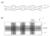
1A・・・繊維束
1S・・・繊維布
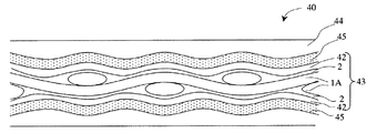
2・・・樹脂層
3・・・樹脂含浸繊維布(複合体層)
10、20、30・・・繊維充填系透明プラスチック基板
13、23、33、43・・・樹脂含浸繊維布を含む複合体層
14、24、34、44・・・平坦化樹脂層
15、25、35、45・・・無機バリア層
16、26・・・液晶層
17、27・・・繊維充填系プラスチック基板
36・・・陽極
37・・・有機発光層
38・・・陰極
100、200・・・液晶表示装置
300・・・有機EL表示装置
Claims (8)
- 樹脂が含浸された繊維布を含む複合体層と、前記複合体層上に形成された無機バリア層と、前記無機バリア層上に形成された平坦化樹脂層とを有する第1プラスチック基板と、
前記第1基板の前記平坦化樹脂層側に設けられた表示媒体層と、
を有する、表示装置。 - 前記表示媒体層を介して前記第1基板に対向するように配置された第2プラスチック基板を有し、前記第2基板は、前記第1基板と同じ構成を有する、請求項1に記載の表示装置。
- 前記表示媒体層は、有機発光層を含む、請求項1または2に記載の表示装置。
- 前記表示媒体層は、液晶層である、請求項1または2に記載の表示装置。
- 前記無機バリア層は、前記複合体層の前記表示媒体層に対向する領域の全体を覆う、請求項4に記載の表示装置。
- 請求項1から5のいずれかに記載の表示装置の製造方法であって、
前記第1および第2プラスチック基板を製造するプロセスが、
樹脂が含浸された繊維布を含む複合体層を用意する工程と、
前記複合体層の表面に薄膜堆積法を用いて、第1の温度で無機バリア層を形成する工程と、
前記無機バリア層上に、前記第1の温度よりも低い第2の温度で前記平坦化樹脂層を形成する工程と、
を包含する、表示装置の製造方法。 - 前記第1の温度が200℃以上である、請求項6に記載の表示装置の製造方法。
- 前記無機バリア層は、二酸化ケイ素を含む、請求項6または7に記載の表示装置の製造方法。
Priority Applications (4)
| Application Number | Priority Date | Filing Date | Title |
|---|---|---|---|
| JP2003377069A JP4233433B2 (ja) | 2003-11-06 | 2003-11-06 | 表示装置の製造方法 |
| US10/979,724 US7378137B2 (en) | 2003-11-06 | 2004-11-02 | Display device |
| US11/859,093 US7651745B2 (en) | 2003-11-06 | 2007-09-21 | Display device |
| US12/099,196 US7923062B2 (en) | 2003-11-06 | 2008-04-08 | Display device |
Applications Claiming Priority (1)
| Application Number | Priority Date | Filing Date | Title |
|---|---|---|---|
| JP2003377069A JP4233433B2 (ja) | 2003-11-06 | 2003-11-06 | 表示装置の製造方法 |
Related Child Applications (1)
| Application Number | Title | Priority Date | Filing Date |
|---|---|---|---|
| JP2008293687A Division JP2009058974A (ja) | 2008-11-17 | 2008-11-17 | 表示装置 |
Publications (2)
| Publication Number | Publication Date |
|---|---|
| JP2005140976A true JP2005140976A (ja) | 2005-06-02 |
| JP4233433B2 JP4233433B2 (ja) | 2009-03-04 |
Family
ID=34687913
Family Applications (1)
| Application Number | Title | Priority Date | Filing Date |
|---|---|---|---|
| JP2003377069A Expired - Fee Related JP4233433B2 (ja) | 2003-11-06 | 2003-11-06 | 表示装置の製造方法 |
Country Status (2)
| Country | Link |
|---|---|
| US (3) | US7378137B2 (ja) |
| JP (1) | JP4233433B2 (ja) |
Cited By (15)
| Publication number | Priority date | Publication date | Assignee | Title |
|---|---|---|---|---|
| JP2006243393A (ja) * | 2005-03-03 | 2006-09-14 | Sharp Corp | 表示装置用プラスチック基板およびその製造方法 |
| WO2008044397A1 (en) * | 2006-10-11 | 2008-04-17 | Sumitomo Bakelite Co., Ltd. | Transparent composite sheet |
| JP2008216541A (ja) * | 2007-03-02 | 2008-09-18 | Sumitomo Bakelite Co Ltd | 透明電極付複合材料基板 |
| JPWO2007144995A1 (ja) * | 2006-06-15 | 2009-10-29 | シャープ株式会社 | 表示装置及びその製造方法 |
| JP2010050173A (ja) * | 2008-08-20 | 2010-03-04 | Semiconductor Energy Lab Co Ltd | 発光装置及び電子機器 |
| JP2010182668A (ja) * | 2009-01-08 | 2010-08-19 | Semiconductor Energy Lab Co Ltd | 発光装置及び電子機器 |
| JP2010191267A (ja) * | 2009-02-19 | 2010-09-02 | Fuji Xerox Co Ltd | 画像表示媒体および画像表示装置 |
| JP2012227153A (ja) * | 2012-07-10 | 2012-11-15 | Semiconductor Energy Lab Co Ltd | 発光装置及び発光装置の作製方法 |
| US8415003B2 (en) | 2009-04-28 | 2013-04-09 | Cheil Industries Inc. | Flexible substrate for display panel and manufacturing method thereof |
| JP2014146610A (ja) * | 2014-04-08 | 2014-08-14 | Semiconductor Energy Lab Co Ltd | 発光装置 |
| WO2014148482A1 (ja) * | 2013-03-19 | 2014-09-25 | 住友ベークライト株式会社 | 面光源用基板、面光源照明装置および面光源用基板の製造方法 |
| US8941011B2 (en) | 2011-08-16 | 2015-01-27 | Samsung Display Co., Ltd. | Flexible substrates and method of manufacturing the same |
| JP2016012576A (ja) * | 2008-07-10 | 2016-01-21 | 株式会社半導体エネルギー研究所 | モジュール |
| JP2016106348A (ja) * | 2013-08-02 | 2016-06-16 | 住友ベークライト株式会社 | 面光源用基板、面光源照明および面光源用基板の製造方法 |
| JP2021082835A (ja) * | 2008-04-25 | 2021-05-27 | 株式会社半導体エネルギー研究所 | 半導体装置 |
Families Citing this family (21)
| Publication number | Priority date | Publication date | Assignee | Title |
|---|---|---|---|---|
| JP4233433B2 (ja) * | 2003-11-06 | 2009-03-04 | シャープ株式会社 | 表示装置の製造方法 |
| JP4063225B2 (ja) * | 2004-01-21 | 2008-03-19 | ソニー株式会社 | 液晶表示装置および液晶表示装置の製造方法 |
| JP4378314B2 (ja) * | 2005-04-26 | 2009-12-02 | シャープ株式会社 | 表示装置及び表示装置の製造方法 |
| US7678701B2 (en) * | 2006-07-31 | 2010-03-16 | Eastman Kodak Company | Flexible substrate with electronic devices formed thereon |
| KR20100037117A (ko) * | 2007-07-03 | 2010-04-08 | 쓰리엠 이노베이티브 프로퍼티즈 컴파니 | 투과성 광학 필름을 갖는 백라이트 조립체 |
| KR20090114171A (ko) * | 2008-04-29 | 2009-11-03 | 삼성전자주식회사 | 표시 장치 |
| TWI475282B (zh) * | 2008-07-10 | 2015-03-01 | Semiconductor Energy Lab | 液晶顯示裝置和其製造方法 |
| KR101560772B1 (ko) | 2008-09-17 | 2015-10-16 | 삼성디스플레이 주식회사 | 표시장치 및 그 제조방법 |
| JP2010181777A (ja) * | 2009-02-09 | 2010-08-19 | Hitachi Displays Ltd | 表示装置 |
| JP2011197402A (ja) * | 2010-03-19 | 2011-10-06 | Asahi Glass Co Ltd | 液晶表示パネル、ガラス基板、および液晶表示パネルの製造方法 |
| KR101332442B1 (ko) * | 2011-09-21 | 2013-11-25 | 제일모직주식회사 | 복합시트 및 이를 포함하는 표시소자용 기판 |
| KR101887217B1 (ko) * | 2012-01-06 | 2018-08-10 | 삼성디스플레이 주식회사 | 표시 장치 및 표시 장치의 제조 방법 |
| KR20130129675A (ko) * | 2012-05-21 | 2013-11-29 | 삼성디스플레이 주식회사 | 표시판 및 이를 포함하는 표시 장치 |
| US9701068B2 (en) | 2012-07-27 | 2017-07-11 | Apple Inc. | Transparent fiber composite |
| CN107425030B (zh) * | 2012-08-20 | 2020-11-06 | 赫普塔冈微光有限公司 | 光学晶片的制造 |
| TWI488025B (zh) * | 2012-08-31 | 2015-06-11 | Quanta Comp Inc | 電子裝置之殼體及其製法 |
| KR20140139299A (ko) * | 2013-05-27 | 2014-12-05 | 삼성디스플레이 주식회사 | 디스플레이 장치용 윈도우 구조체 및 이를 구비한 디스플레이 장치 |
| JP6463662B2 (ja) * | 2015-10-06 | 2019-02-06 | 信越化学工業株式会社 | 半導体封止用基材付封止材、半導体封止用基材付封止材の製造方法、及び半導体装置の製造方法 |
| CN113327996B (zh) * | 2021-05-27 | 2022-06-10 | 福斯特(嘉兴)新材料有限公司 | 一种透明背板 |
| KR20230010076A (ko) * | 2021-07-08 | 2023-01-18 | 삼성디스플레이 주식회사 | 폴더블 표시 장치와 그의 제조 방법 |
| CN114038321B (zh) * | 2021-11-22 | 2023-10-17 | 深圳市华星光电半导体显示技术有限公司 | 显示器 |
Family Cites Families (34)
| Publication number | Priority date | Publication date | Assignee | Title |
|---|---|---|---|---|
| US3789049A (en) * | 1970-12-23 | 1974-01-29 | Nitto Boseki Co Ltd | Glass fiber-reinforced epoxy resin or polyester resin composition and method for manufacturing same |
| US4917471A (en) * | 1986-08-30 | 1990-04-17 | Canon Kabushiki Kaisha | Liquid crystal device |
| US5009922A (en) * | 1989-03-02 | 1991-04-23 | Ashahi Glass Company, Ltd. | Method of forming a transparent conductive film |
| US5689322A (en) * | 1993-07-30 | 1997-11-18 | Sharp Kabushiki Kaisha | Liquid crystal display device having regions with different twist angles |
| US5936850A (en) * | 1995-03-03 | 1999-08-10 | Canon Kabushiki Kaisha | Circuit board connection structure and method, and liquid crystal device including the connection structure |
| US5739180A (en) * | 1996-05-02 | 1998-04-14 | Lucent Technologies Inc. | Flat panel displays and methods and substrates therefor |
| US5789848A (en) * | 1996-08-02 | 1998-08-04 | Motorola, Inc. | Field emission display having a cathode reinforcement member |
| JPH112812A (ja) | 1997-06-12 | 1999-01-06 | Toshiba Corp | 反射型導電性基板、反射型液晶表示装置、及び反射型導電性基板の製造方法 |
| DE69840914D1 (de) * | 1997-10-14 | 2009-07-30 | Patterning Technologies Ltd | Methode zur Herstellung eines elektrischen Kondensators |
| US6753047B1 (en) * | 1999-06-10 | 2004-06-22 | Ppg Industries Ohio, Inc. | Electrodes for liquid crystal cells |
| US6413645B1 (en) * | 2000-04-20 | 2002-07-02 | Battelle Memorial Institute | Ultrabarrier substrates |
| JP2001133761A (ja) | 1999-11-04 | 2001-05-18 | Toshiba Corp | 液晶表示素子及び有機led素子 |
| JP3752949B2 (ja) * | 2000-02-28 | 2006-03-08 | 日立化成工業株式会社 | 配線基板及び半導体装置 |
| US20010038894A1 (en) * | 2000-03-14 | 2001-11-08 | Minoru Komada | Gas barrier film |
| US6492026B1 (en) * | 2000-04-20 | 2002-12-10 | Battelle Memorial Institute | Smoothing and barrier layers on high Tg substrates |
| JP2002080616A (ja) | 2000-06-30 | 2002-03-19 | Sumitomo Bakelite Co Ltd | 表示素子用高分子フィルム及びこれを用いた表示素子用基板 |
| JP2002116455A (ja) | 2000-08-01 | 2002-04-19 | Kyodo Printing Co Ltd | 液晶表示装置、液晶表示装置の電極基材及び液晶表示装置の製造方法 |
| US6358664B1 (en) * | 2000-09-15 | 2002-03-19 | 3M Innovative Properties Company | Electronically active primer layers for thermal patterning of materials for electronic devices |
| US20020110673A1 (en) * | 2001-02-14 | 2002-08-15 | Ramin Heydarpour | Multilayered electrode/substrate structures and display devices incorporating the same |
| SG102681A1 (en) | 2001-02-19 | 2004-03-26 | Semiconductor Energy Lab | Light emitting device and method of manufacturing the same |
| US6590346B1 (en) * | 2001-07-16 | 2003-07-08 | Alien Technology Corporation | Double-metal background driven displays |
| US6556470B1 (en) * | 2001-07-31 | 2003-04-29 | Hewlett-Packard Company | Field addressable rewritable media |
| JP2003048279A (ja) | 2001-08-07 | 2003-02-18 | Sumitomo Bakelite Co Ltd | 高分子シートの製造方法およびこれを用いた高分子シート |
| JP2003050384A (ja) | 2001-08-07 | 2003-02-21 | Sumitomo Bakelite Co Ltd | 反射型液晶表示素子用プラスチック基板 |
| JP2003048293A (ja) | 2001-08-07 | 2003-02-18 | Sumitomo Bakelite Co Ltd | 多層樹脂シート |
| JP2003084264A (ja) | 2001-09-11 | 2003-03-19 | Sumitomo Bakelite Co Ltd | 反射型液晶表示素子用プラスチック基板。 |
| JP2003098512A (ja) | 2001-09-26 | 2003-04-03 | Sumitomo Bakelite Co Ltd | 反射型液晶表示素子用プラスチック基板。 |
| JP2003297556A (ja) | 2002-04-02 | 2003-10-17 | Dainippon Printing Co Ltd | 表示素子用基材、表示パネル、表示装置及び表示素子用基材の製造方法 |
| JP2005523976A (ja) * | 2002-04-26 | 2005-08-11 | イー・アイ・デュポン・ドウ・ヌムール・アンド・カンパニー | プリント回路基板および集積回路チップパッケージ用低損失誘電材料 |
| KR20050004876A (ko) | 2002-05-27 | 2005-01-12 | 닛토덴코 가부시키가이샤 | 수지 시트, 이것을 사용한 액정 셀 기판 |
| US6853478B2 (en) * | 2002-06-13 | 2005-02-08 | Hewlett-Packard Development Company, L.P. | Color display with molecular light valve |
| JP4181060B2 (ja) * | 2003-02-25 | 2008-11-12 | シャープ株式会社 | 液晶表示装置 |
| JP5196705B2 (ja) | 2003-03-26 | 2013-05-15 | 住友ベークライト株式会社 | 光学シート |
| JP4233433B2 (ja) | 2003-11-06 | 2009-03-04 | シャープ株式会社 | 表示装置の製造方法 |
-
2003
- 2003-11-06 JP JP2003377069A patent/JP4233433B2/ja not_active Expired - Fee Related
-
2004
- 2004-11-02 US US10/979,724 patent/US7378137B2/en not_active Expired - Fee Related
-
2007
- 2007-09-21 US US11/859,093 patent/US7651745B2/en not_active Expired - Fee Related
-
2008
- 2008-04-08 US US12/099,196 patent/US7923062B2/en not_active Expired - Fee Related
Cited By (24)
| Publication number | Priority date | Publication date | Assignee | Title |
|---|---|---|---|---|
| JP2006243393A (ja) * | 2005-03-03 | 2006-09-14 | Sharp Corp | 表示装置用プラスチック基板およびその製造方法 |
| JPWO2007144995A1 (ja) * | 2006-06-15 | 2009-10-29 | シャープ株式会社 | 表示装置及びその製造方法 |
| WO2008044397A1 (en) * | 2006-10-11 | 2008-04-17 | Sumitomo Bakelite Co., Ltd. | Transparent composite sheet |
| JP2008216541A (ja) * | 2007-03-02 | 2008-09-18 | Sumitomo Bakelite Co Ltd | 透明電極付複合材料基板 |
| JP2021082835A (ja) * | 2008-04-25 | 2021-05-27 | 株式会社半導体エネルギー研究所 | 半導体装置 |
| JP7150908B2 (ja) | 2008-04-25 | 2022-10-11 | 株式会社半導体エネルギー研究所 | 半導体装置 |
| US11908976B2 (en) | 2008-07-10 | 2024-02-20 | Semiconductor Energy Laboratory Co., Ltd. | Light emitting device and electronic device |
| US11557697B2 (en) | 2008-07-10 | 2023-01-17 | Semiconductor Energy Laboratory Co., Ltd. | Flexible light emitting device comprising a polyimide resin |
| US11101407B2 (en) | 2008-07-10 | 2021-08-24 | Semiconductor Energy Laboratory Co., Ltd. | Light emitting device sealed in a fibrous body to improve manufacturability and electronic device including the light emitting device |
| US10079330B2 (en) | 2008-07-10 | 2018-09-18 | Semiconductor Energy Laboratory Co., Ltd. | Light emitting device and electronic device having an embedded pixel electrode |
| US10205062B2 (en) | 2008-07-10 | 2019-02-12 | Semiconductor Energy Laboratory Co., Ltd. | Light emitting device that is highly reliable, thin and is not damaged by external local pressure and electronic device |
| JP2016012576A (ja) * | 2008-07-10 | 2016-01-21 | 株式会社半導体エネルギー研究所 | モジュール |
| JP2010050173A (ja) * | 2008-08-20 | 2010-03-04 | Semiconductor Energy Lab Co Ltd | 発光装置及び電子機器 |
| US10361258B2 (en) | 2009-01-08 | 2019-07-23 | Semiconductor Energy Laboratory Co., Ltd. | Light emitting device and electronic device |
| US9929220B2 (en) | 2009-01-08 | 2018-03-27 | Semiconductor Energy Laboratory Co., Ltd. | Light emitting device and electronic device |
| JP2010182668A (ja) * | 2009-01-08 | 2010-08-19 | Semiconductor Energy Lab Co Ltd | 発光装置及び電子機器 |
| JP2010191267A (ja) * | 2009-02-19 | 2010-09-02 | Fuji Xerox Co Ltd | 画像表示媒体および画像表示装置 |
| US8415003B2 (en) | 2009-04-28 | 2013-04-09 | Cheil Industries Inc. | Flexible substrate for display panel and manufacturing method thereof |
| US9480165B2 (en) | 2011-08-16 | 2016-10-25 | Samsung Display Co., Ltd. | Flexible substrates and method of manufacturing the same |
| US8941011B2 (en) | 2011-08-16 | 2015-01-27 | Samsung Display Co., Ltd. | Flexible substrates and method of manufacturing the same |
| JP2012227153A (ja) * | 2012-07-10 | 2012-11-15 | Semiconductor Energy Lab Co Ltd | 発光装置及び発光装置の作製方法 |
| WO2014148482A1 (ja) * | 2013-03-19 | 2014-09-25 | 住友ベークライト株式会社 | 面光源用基板、面光源照明装置および面光源用基板の製造方法 |
| JP2016106348A (ja) * | 2013-08-02 | 2016-06-16 | 住友ベークライト株式会社 | 面光源用基板、面光源照明および面光源用基板の製造方法 |
| JP2014146610A (ja) * | 2014-04-08 | 2014-08-14 | Semiconductor Energy Lab Co Ltd | 発光装置 |
Also Published As
| Publication number | Publication date |
|---|---|
| US7378137B2 (en) | 2008-05-27 |
| JP4233433B2 (ja) | 2009-03-04 |
| US7651745B2 (en) | 2010-01-26 |
| US7923062B2 (en) | 2011-04-12 |
| US20080213474A1 (en) | 2008-09-04 |
| US20080013020A1 (en) | 2008-01-17 |
| US20050140861A1 (en) | 2005-06-30 |
Similar Documents
| Publication | Publication Date | Title |
|---|---|---|
| JP4233433B2 (ja) | 表示装置の製造方法 | |
| US20090153961A1 (en) | Grid Polarizer and Method for Manufacturing the Same | |
| US8149377B2 (en) | Tunable-focusing liquid crystal lens cell and method of fabrication thereof | |
| KR100794239B1 (ko) | 플라스틱 기판 및 그것을 구비한 액정 표시 장치 | |
| JP4181013B2 (ja) | 表示装置およびその製造方法 | |
| JP2004515824A (ja) | スタックドリキッドセル | |
| KR102460687B1 (ko) | 플렉서블 표시 장치 | |
| US11402550B2 (en) | Flexible polarizing cover plate having hard coating with ink-filled grooves and preparation method thereof | |
| US12009371B2 (en) | Display device with transparent electric insulating heat conductive protective layer and production method thereof | |
| JP2004280071A (ja) | 液晶表示装置 | |
| JP2001133761A (ja) | 液晶表示素子及び有機led素子 | |
| US8717529B2 (en) | Display apparatus and method of fabricating the same | |
| JP4393077B2 (ja) | 透明基板 | |
| KR101051634B1 (ko) | 디스플레이 패널용 플렉서블 기판 및 그 제조 방법 | |
| US20100059757A1 (en) | Apparatus and method of manufacturing the same | |
| JP2015215388A (ja) | 表示装置 | |
| JP2009058974A (ja) | 表示装置 | |
| JP4484733B2 (ja) | 表示装置用プラスチック基板およびその製造方法 | |
| US20100075124A1 (en) | Apparatus having planarized substrate and method of manufacturing the same | |
| KR102598479B1 (ko) | 플렉서블 기판과 이를 포함하는 플렉서블 표시장치 | |
| CN1877411A (zh) | 广视角可挠式彩色化显示器及制造方法 | |
| JP2022143725A (ja) | 車両用合わせガラス | |
| JP2001228468A (ja) | カラー液晶表示素子の製造方法 | |
| JP2015099236A (ja) | 液晶装置、及び液晶装置の製造方法 | |
| KR20080001526A (ko) | 액정 표시장치 및 그 제조 방법 |
Legal Events
| Date | Code | Title | Description |
|---|---|---|---|
| A977 | Report on retrieval |
Free format text: JAPANESE INTERMEDIATE CODE: A971007 Effective date: 20060124 |
|
| A131 | Notification of reasons for refusal |
Free format text: JAPANESE INTERMEDIATE CODE: A131 Effective date: 20070522 |
|
| A521 | Request for written amendment filed |
Free format text: JAPANESE INTERMEDIATE CODE: A523 Effective date: 20070719 |
|
| A131 | Notification of reasons for refusal |
Free format text: JAPANESE INTERMEDIATE CODE: A131 Effective date: 20080115 |
|
| A02 | Decision of refusal |
Free format text: JAPANESE INTERMEDIATE CODE: A02 Effective date: 20080610 |
|
| A521 | Request for written amendment filed |
Free format text: JAPANESE INTERMEDIATE CODE: A523 Effective date: 20080807 |
|
| A911 | Transfer to examiner for re-examination before appeal (zenchi) |
Free format text: JAPANESE INTERMEDIATE CODE: A911 Effective date: 20080815 |
|
| A131 | Notification of reasons for refusal |
Free format text: JAPANESE INTERMEDIATE CODE: A131 Effective date: 20080916 |
|
| A521 | Request for written amendment filed |
Free format text: JAPANESE INTERMEDIATE CODE: A523 Effective date: 20081117 |
|
| TRDD | Decision of grant or rejection written | ||
| A01 | Written decision to grant a patent or to grant a registration (utility model) |
Free format text: JAPANESE INTERMEDIATE CODE: A01 Effective date: 20081209 |
|
| A01 | Written decision to grant a patent or to grant a registration (utility model) |
Free format text: JAPANESE INTERMEDIATE CODE: A01 |
|
| A61 | First payment of annual fees (during grant procedure) |
Free format text: JAPANESE INTERMEDIATE CODE: A61 Effective date: 20081209 |
|
| FPAY | Renewal fee payment (event date is renewal date of database) |
Free format text: PAYMENT UNTIL: 20111219 Year of fee payment: 3 |
|
| R150 | Certificate of patent or registration of utility model |
Free format text: JAPANESE INTERMEDIATE CODE: R150 |
|
| FPAY | Renewal fee payment (event date is renewal date of database) |
Free format text: PAYMENT UNTIL: 20111219 Year of fee payment: 3 |
|
| FPAY | Renewal fee payment (event date is renewal date of database) |
Free format text: PAYMENT UNTIL: 20121219 Year of fee payment: 4 |
|
| LAPS | Cancellation because of no payment of annual fees |