JP2005166251A - メモリデバイス - Google Patents
メモリデバイス Download PDFInfo
- Publication number
- JP2005166251A JP2005166251A JP2004349802A JP2004349802A JP2005166251A JP 2005166251 A JP2005166251 A JP 2005166251A JP 2004349802 A JP2004349802 A JP 2004349802A JP 2004349802 A JP2004349802 A JP 2004349802A JP 2005166251 A JP2005166251 A JP 2005166251A
- Authority
- JP
- Japan
- Prior art keywords
- memory cell
- category
- resistance state
- value
- count
- Prior art date
- Legal status (The legal status is an assumption and is not a legal conclusion. Google has not performed a legal analysis and makes no representation as to the accuracy of the status listed.)
- Withdrawn
Links
Images




Classifications
-
- G—PHYSICS
- G11—INFORMATION STORAGE
- G11C—STATIC STORES
- G11C11/00—Digital stores characterised by the use of particular electric or magnetic storage elements; Storage elements therefor
- G11C11/02—Digital stores characterised by the use of particular electric or magnetic storage elements; Storage elements therefor using magnetic elements
- G11C11/16—Digital stores characterised by the use of particular electric or magnetic storage elements; Storage elements therefor using magnetic elements using elements in which the storage effect is based on magnetic spin effect
-
- G—PHYSICS
- G11—INFORMATION STORAGE
- G11C—STATIC STORES
- G11C29/00—Checking stores for correct operation ; Subsequent repair; Testing stores during standby or offline operation
- G11C29/02—Detection or location of defective auxiliary circuits, e.g. defective refresh counters
-
- G—PHYSICS
- G11—INFORMATION STORAGE
- G11C—STATIC STORES
- G11C29/00—Checking stores for correct operation ; Subsequent repair; Testing stores during standby or offline operation
- G11C29/02—Detection or location of defective auxiliary circuits, e.g. defective refresh counters
- G11C29/026—Detection or location of defective auxiliary circuits, e.g. defective refresh counters in sense amplifiers
-
- G—PHYSICS
- G11—INFORMATION STORAGE
- G11C—STATIC STORES
- G11C29/00—Checking stores for correct operation ; Subsequent repair; Testing stores during standby or offline operation
- G11C29/02—Detection or location of defective auxiliary circuits, e.g. defective refresh counters
- G11C29/028—Detection or location of defective auxiliary circuits, e.g. defective refresh counters with adaption or trimming of parameters
Landscapes
- Engineering & Computer Science (AREA)
- Computer Hardware Design (AREA)
- Mram Or Spin Memory Techniques (AREA)
- Semiconductor Memories (AREA)
- For Increasing The Reliability Of Semiconductor Memories (AREA)
- Hall/Mr Elements (AREA)
Abstract
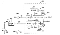
メモリセルの状態に応じて適切な大きさの読出し電流でメモリセルを読み出すように読出し回路を較正する方法および装置を提供すること。
【解決手段】
本発明の実施形態によれば磁気メモリ(20)が得られる。一実施形態において磁気メモリ(20)は、抵抗状態を提供するように構成されたメモリセル(26)のアレイ(22)と、読出し回路(24)とを備える。読出し回路(24)は、メモリセルアレイ(22)内のメモリセル(26)の抵抗値を検出し、検出結果を得て、その検出結果を、抵抗状態間に位置する中央領域を含む少なくとも3つの異なるカテゴリのうちの1つに分類するように構成される。
【選択図】図1
Description
22 メモリセルアレイ
24 読出し回路
26 磁気メモリセル
300 範囲外高カテゴリ
302 高抵抗領域カテゴリ
304 曖昧領域
306 低抵抗状態カテゴリ
308 範囲外低カテゴリ
Claims (10)
- 抵抗状態を提供するように構成されたメモリセル(22)のアレイと、
前記メモリセル(22)のアレイ内の1つのメモリセル(26)の抵抗値を検出し、検出結果を得て、該検出結果を前記抵抗状態間に位置する中央カテゴリ(304)を含む少なくとも3つの異なるカテゴリのうちの1つに分類するように構成された読出し回路(24)と、
からなる磁気メモリ(20)。 - 前記少なくとも3つの異なるカテゴリは低抵抗状態カテゴリ(306)および高抵抗状態カテゴリ(302)を含み、前記中央カテゴリ(304)は前記低抵抗状態カテゴリ(306)と前記高抵抗状態カテゴリ(302)との間に位置する、請求項1に記載の磁気メモリ。
- 前記少なくとも3つの異なるカテゴリは、低抵抗状態カテゴリ(306)、高抵抗状態カテゴリ(302)、範囲外低カテゴリ(308)、および範囲外高カテゴリ(300)を含む5つのカテゴリを含む、請求項1に記載の磁気メモリ。
- 前記読出し回路(24)は、複数の検出動作からなる読出し動作を実施して前記検出結果を得るように構成され、短絡されたメモリセルからの前記検出結果は、前記中央領域(304)に分類される、請求項1に記載の磁気メモリ。
- 前記読出し回路(24)は、複数の検出動作を含む読出し動作を実施して前記検出結果を得るように構成され、開放されたメモリセルからの前記検出結果は、前記中央領域(304)に分類される、請求項1に記載の磁気メモリ。
- 前記読出し回路(24)は、前記検出結果のカテゴリを示すフラグを出力するとともに、論理レベルを出力するように構成される、請求項1に記載の磁気メモリ。
- 前記読出し回路(24)は、第1の検出動作の後に、前記検出結果を分類するように構成される、請求項1に記載の磁気メモリ。
- 磁気メモリ(20)を読み出す方法であって、
前記磁気メモリ(20)のメモリセル(26)の抵抗値を検出し、正味の検出結果値を得るステップと、
前記正味の検出結果値を低抵抗状態領域(306)、高抵抗状態領域(302)、および該低抵抗状態領域(306)と該高抵抗状態領域(302)との間に位置する中央領域(304)を含む複数の異なる抵抗領域に分類するステップと、
からなる方法。 - 前記メモリセル(26)の抵抗値を検出するステップは、3つの検出動作を含む多段検出読出し動作を含み、
前記正味の検出結果値を分類するステップは、前記正味の検出結果値を閾値と比較し、前記検出結果値の領域を示すフラグを出力することを含む、請求項8に記載の方法。 - 前記メモリセル(26)を検出して第1の検出結果を得るステップと、
前記第1の検出結果を即時較正領域および遅延較正領域を含む複数の領域に分類するステップと、
前記第1の検出結果が開放であった場合および前記第1の検出結果が短絡であった場合は即時較正応答を実施し、前記第1の検出結果が短絡値と低抵抗状態値との間にあった場合および前記第1の検出結果が開放値と高抵抗状態値との間にあった場合は、遅延較正応答を実施することを含む、前記第1の検出結果のカテゴリに基づいて応答するステップと、
を含む、請求項8に記載の方法。
Applications Claiming Priority (1)
| Application Number | Priority Date | Filing Date | Title |
|---|---|---|---|
| US10/727,273 US6999366B2 (en) | 2003-12-03 | 2003-12-03 | Magnetic memory including a sense result category between logic states |
Publications (1)
| Publication Number | Publication Date |
|---|---|
| JP2005166251A true JP2005166251A (ja) | 2005-06-23 |
Family
ID=34633453
Family Applications (1)
| Application Number | Title | Priority Date | Filing Date |
|---|---|---|---|
| JP2004349802A Withdrawn JP2005166251A (ja) | 2003-12-03 | 2004-12-02 | メモリデバイス |
Country Status (3)
| Country | Link |
|---|---|
| US (1) | US6999366B2 (ja) |
| JP (1) | JP2005166251A (ja) |
| DE (1) | DE102004037834A1 (ja) |
Cited By (4)
| Publication number | Priority date | Publication date | Assignee | Title |
|---|---|---|---|---|
| JP2012181900A (ja) * | 2011-03-02 | 2012-09-20 | Toshiba Corp | 半導体記憶装置およびそのテスト方法 |
| KR101447819B1 (ko) * | 2013-05-08 | 2014-10-10 | 한양대학교 산학협력단 | 마그네틱 메모리의 테스트 방법 |
| JP2015515711A (ja) * | 2012-03-30 | 2015-05-28 | シリコン ストーリッジ テクノロージー インコーポレイテッドSilicon Storage Technology, Inc. | オンザフライ(on−the−fly)でトリミング可能なセンス増幅器 |
| US11875834B2 (en) | 2020-09-17 | 2024-01-16 | Kioxia Corporation | Magnetic memory device and memory system |
Families Citing this family (38)
| Publication number | Priority date | Publication date | Assignee | Title |
|---|---|---|---|---|
| JP5792918B2 (ja) * | 2000-08-14 | 2015-10-14 | サンディスク・スリー・ディ・リミテッド・ライアビリティ・カンパニーSandisk 3D Llc | 高集積メモリデバイス |
| US8008700B2 (en) * | 2002-12-19 | 2011-08-30 | Sandisk 3D Llc | Non-volatile memory cell with embedded antifuse |
| US7618850B2 (en) * | 2002-12-19 | 2009-11-17 | Sandisk 3D Llc | Method of making a diode read/write memory cell in a programmed state |
| US7800933B2 (en) * | 2005-09-28 | 2010-09-21 | Sandisk 3D Llc | Method for using a memory cell comprising switchable semiconductor memory element with trimmable resistance |
| US20070164388A1 (en) * | 2002-12-19 | 2007-07-19 | Sandisk 3D Llc | Memory cell comprising a diode fabricated in a low resistivity, programmed state |
| US7800932B2 (en) * | 2005-09-28 | 2010-09-21 | Sandisk 3D Llc | Memory cell comprising switchable semiconductor memory element with trimmable resistance |
| US7660181B2 (en) * | 2002-12-19 | 2010-02-09 | Sandisk 3D Llc | Method of making non-volatile memory cell with embedded antifuse |
| DE102005001667B4 (de) * | 2005-01-13 | 2011-04-21 | Qimonda Ag | Nichtflüchtige Speicherzelle zum Speichern eines Datums in einer integrierten Schaltung |
| US7457155B2 (en) * | 2006-08-31 | 2008-11-25 | Micron Technology, Inc. | Non-volatile memory device and method having bit-state assignments selected to minimize signal coupling |
| US7379364B2 (en) * | 2006-10-19 | 2008-05-27 | Unity Semiconductor Corporation | Sensing a signal in a two-terminal memory array having leakage current |
| US7372753B1 (en) * | 2006-10-19 | 2008-05-13 | Unity Semiconductor Corporation | Two-cycle sensing in a two-terminal memory array having leakage current |
| US7742329B2 (en) * | 2007-03-06 | 2010-06-22 | Qualcomm Incorporated | Word line transistor strength control for read and write in spin transfer torque magnetoresistive random access memory |
| US8004880B2 (en) * | 2007-03-06 | 2011-08-23 | Qualcomm Incorporated | Read disturb reduction circuit for spin transfer torque magnetoresistive random access memory |
| WO2008121553A1 (en) * | 2007-03-29 | 2008-10-09 | Sandisk Corporation | Non-volatile storage with decoding of data using reliability metrics based on multiple reads |
| US7904793B2 (en) * | 2007-03-29 | 2011-03-08 | Sandisk Corporation | Method for decoding data in non-volatile storage using reliability metrics based on multiple reads |
| US7966550B2 (en) * | 2007-03-31 | 2011-06-21 | Sandisk Technologies Inc. | Soft bit data transmission for error correction control in non-volatile memory |
| US7975209B2 (en) * | 2007-03-31 | 2011-07-05 | Sandisk Technologies Inc. | Non-volatile memory with guided simulated annealing error correction control |
| US7971127B2 (en) * | 2007-03-31 | 2011-06-28 | Sandisk Technologies Inc. | Guided simulated annealing in non-volatile memory error correction control |
| US7966546B2 (en) * | 2007-03-31 | 2011-06-21 | Sandisk Technologies Inc. | Non-volatile memory with soft bit data transmission for error correction control |
| US7706169B2 (en) * | 2007-12-27 | 2010-04-27 | Sandisk 3D Llc | Large capacity one-time programmable memory cell using metal oxides |
| US7764534B2 (en) | 2007-12-28 | 2010-07-27 | Sandisk 3D Llc | Two terminal nonvolatile memory using gate controlled diode elements |
| US7830698B2 (en) * | 2008-04-11 | 2010-11-09 | Sandisk 3D Llc | Multilevel nonvolatile memory device containing a carbon storage material and methods of making and using same |
| US7812335B2 (en) * | 2008-04-11 | 2010-10-12 | Sandisk 3D Llc | Sidewall structured switchable resistor cell |
| US7719876B2 (en) | 2008-07-31 | 2010-05-18 | Unity Semiconductor Corporation | Preservation circuit and methods to maintain values representing data in one or more layers of memory |
| US7830701B2 (en) * | 2008-09-19 | 2010-11-09 | Unity Semiconductor Corporation | Contemporaneous margin verification and memory access for memory cells in cross point memory arrays |
| US8509003B2 (en) * | 2011-09-20 | 2013-08-13 | Taiwan Semiconductor Manufacturing Co., Ltd. | Read architecture for MRAM |
| US9128869B2 (en) | 2011-09-29 | 2015-09-08 | Micron Technology, Inc. | Systems and methods involving managing a problematic memory cell |
| IN2014CH00519A (ja) * | 2013-12-02 | 2015-06-12 | Sandisk Technologies Inc | |
| US9711240B2 (en) * | 2015-01-08 | 2017-07-18 | Kabushiki Kaisha Toshiba | Memory system |
| KR102565297B1 (ko) * | 2016-10-17 | 2023-08-10 | 엘지디스플레이 주식회사 | 터치 표시 장치, 터치 시스템, 터치 마스터 및 통신 방법 |
| US9806256B1 (en) | 2016-10-21 | 2017-10-31 | Sandisk Technologies Llc | Resistive memory device having sidewall spacer electrode and method of making thereof |
| US9953726B1 (en) * | 2016-11-28 | 2018-04-24 | Arm Limited | Fast quasi-parity checker for correlated electron switch (CES) memory array |
| US10304550B1 (en) | 2017-11-29 | 2019-05-28 | Sandisk Technologies Llc | Sense amplifier with negative threshold sensing for non-volatile memory |
| US10643695B1 (en) | 2019-01-10 | 2020-05-05 | Sandisk Technologies Llc | Concurrent multi-state program verify for non-volatile memory |
| US11024392B1 (en) | 2019-12-23 | 2021-06-01 | Sandisk Technologies Llc | Sense amplifier for bidirectional sensing of memory cells of a non-volatile memory |
| CN113053438B (zh) | 2019-12-27 | 2024-01-30 | 美光科技公司 | 用于确定存取线的电容和电阻特性的装置和方法 |
| US11442091B2 (en) * | 2019-12-27 | 2022-09-13 | Micron Technology, Inc. | Apparatus and methods for determination of capacitive and resistive characteristics of access lines |
| KR102811200B1 (ko) * | 2020-12-15 | 2025-05-23 | 삼성전자주식회사 | 메모리 장치 |
Family Cites Families (11)
| Publication number | Priority date | Publication date | Assignee | Title |
|---|---|---|---|---|
| US23922A (en) * | 1859-05-10 | Machine foe | ||
| US23928A (en) * | 1859-05-10 | Improved bench-plane | ||
| US23923A (en) * | 1859-05-10 | Improvement in railroad-gar brakes | ||
| US23925A (en) * | 1859-05-10 | Apparatus for conducting water to cisterns | ||
| US6262625B1 (en) * | 1999-10-29 | 2001-07-17 | Hewlett-Packard Co | Operational amplifier with digital offset calibration |
| US6188615B1 (en) * | 1999-10-29 | 2001-02-13 | Hewlett-Packard Company | MRAM device including digital sense amplifiers |
| US6584589B1 (en) * | 2000-02-04 | 2003-06-24 | Hewlett-Packard Development Company, L.P. | Self-testing of magneto-resistive memory arrays |
| US6504779B2 (en) * | 2001-05-14 | 2003-01-07 | Hewlett-Packard Company | Resistive cross point memory with on-chip sense amplifier calibration method and apparatus |
| US20030023922A1 (en) | 2001-07-25 | 2003-01-30 | Davis James A. | Fault tolerant magnetoresistive solid-state storage device |
| US7036068B2 (en) | 2001-07-25 | 2006-04-25 | Hewlett-Packard Development Company, L.P. | Error correction coding and decoding in a solid-state storage device |
| US6898134B2 (en) * | 2003-07-18 | 2005-05-24 | Hewlett-Packard Development Company, L.P. | Systems and methods for sensing a memory element |
-
2003
- 2003-12-03 US US10/727,273 patent/US6999366B2/en not_active Expired - Lifetime
-
2004
- 2004-08-04 DE DE102004037834A patent/DE102004037834A1/de not_active Ceased
- 2004-12-02 JP JP2004349802A patent/JP2005166251A/ja not_active Withdrawn
Cited By (4)
| Publication number | Priority date | Publication date | Assignee | Title |
|---|---|---|---|---|
| JP2012181900A (ja) * | 2011-03-02 | 2012-09-20 | Toshiba Corp | 半導体記憶装置およびそのテスト方法 |
| JP2015515711A (ja) * | 2012-03-30 | 2015-05-28 | シリコン ストーリッジ テクノロージー インコーポレイテッドSilicon Storage Technology, Inc. | オンザフライ(on−the−fly)でトリミング可能なセンス増幅器 |
| KR101447819B1 (ko) * | 2013-05-08 | 2014-10-10 | 한양대학교 산학협력단 | 마그네틱 메모리의 테스트 방법 |
| US11875834B2 (en) | 2020-09-17 | 2024-01-16 | Kioxia Corporation | Magnetic memory device and memory system |
Also Published As
| Publication number | Publication date |
|---|---|
| US6999366B2 (en) | 2006-02-14 |
| US20050122767A1 (en) | 2005-06-09 |
| DE102004037834A1 (de) | 2005-07-07 |
Similar Documents
| Publication | Publication Date | Title |
|---|---|---|
| US6999366B2 (en) | Magnetic memory including a sense result category between logic states | |
| JP4048194B2 (ja) | 抵抗性クロスポイントメモリ | |
| US6188615B1 (en) | MRAM device including digital sense amplifiers | |
| US9640239B2 (en) | Sense circuits, semiconductor devices, and related methods for resistance variable memory | |
| US6256247B1 (en) | Differential sense amplifiers for resistive cross point memory cell arrays | |
| US6128239A (en) | MRAM device including analog sense amplifiers | |
| JP4407828B2 (ja) | データの読み出し方法が改善された磁気ランダムアクセスメモリ | |
| US6785156B2 (en) | Method and apparatus for sensing resistance values of memory cells | |
| JP5931105B2 (ja) | Mram感知基準トリミング方法とメモリ装置 | |
| JP4067868B2 (ja) | オンチップセンス増幅器を備える抵抗型クロスポイントメモリの較正方法 | |
| JP4031447B2 (ja) | オフセット調整可能な差動増幅器 | |
| US8036015B2 (en) | Resistive memory | |
| US20060158945A1 (en) | Readout circuit for semiconductor storage device | |
| US6834017B2 (en) | Error detection system for an information storage device | |
| US11521665B2 (en) | Non-volatile memory having write detect circuitry | |
| US6990030B2 (en) | Magnetic memory having a calibration system | |
| US7260004B2 (en) | Method and apparatus for increasing yield in a memory circuit | |
| TWI623939B (zh) | 記憶體裝置與其控制方法 | |
| US6894938B2 (en) | System and method of calibrating a read circuit in a magnetic memory | |
| US7447057B2 (en) | Semiconductor integrated circuit device with a plurality of memory cells storing data | |
| US12224024B2 (en) | Memory with one-time programmable (OTP) cells | |
| KR101136038B1 (ko) | 데이터 저장 디바이스, 메모리 셀 판독 동작 수행 방법 및시스템 | |
| JP4702359B2 (ja) | 半導体記憶装置の読み出し回路 | |
| JP2012256393A (ja) | 半導体記憶装置 |
Legal Events
| Date | Code | Title | Description |
|---|---|---|---|
| A977 | Report on retrieval |
Free format text: JAPANESE INTERMEDIATE CODE: A971007 Effective date: 20070920 |
|
| A131 | Notification of reasons for refusal |
Free format text: JAPANESE INTERMEDIATE CODE: A131 Effective date: 20071002 |
|
| A601 | Written request for extension of time |
Free format text: JAPANESE INTERMEDIATE CODE: A601 Effective date: 20071225 |
|
| A602 | Written permission of extension of time |
Free format text: JAPANESE INTERMEDIATE CODE: A602 Effective date: 20071228 |
|
| A521 | Request for written amendment filed |
Free format text: JAPANESE INTERMEDIATE CODE: A523 Effective date: 20080401 |
|
| A761 | Written withdrawal of application |
Free format text: JAPANESE INTERMEDIATE CODE: A761 Effective date: 20090205 |